NSC LM2702MTX-ADJ, LM2702MT-ADJ Datasheet
LM2702
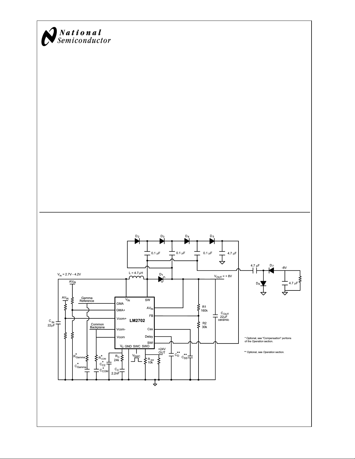
TFT Panel Module
LM2702 TFT Panel Module
November 2002
General Description
The LM2702 is a compact bias solution for TFT displays. It
has a current mode PWM step-up DC/DC converter with a
2A, 0.2Ω internal switch. Capable of generating 8V at
170mA from a Lithium Ion battery, the LM2702 is ideal for
generating bias voltages for large screen LCD panels. The
LM2702 operates at a switching frequency of 600kHz allowing for easy filtering and low noise. An external compensation pin gives the user flexibility in setting frequency compensation, which makes possible the use of small, low ESR
ceramic capacitors at the output. The LM2702 uses a patented internal circuitry to limit startup inrush current of the
boost switching regulator without the use of an external
softstart capacitor. An external softstart pin enables the user
to tailor the softstart to a specific application. The LM2702
has an internal controllable PMOS switch used for controlling the row driver voltages. The switch can be controlled
externally with a control pin and delay time. The LM2702
contains a Vcom amplifier and a Gamma buffer capable of
supplying 50mA source and sink. The TSSOP-16 package
ensures a low profile overall solution.
Typical Application Circuit
Features
n 2A, 0.2Ω, internal power switch
n V
operating range: 2.2V to 12V
IN
n 600kHz switching frequency step-up DC/DC converter
n Inrush current limiting circuitry
n External softstart override
n Internal 7.3Ω PMOS switch
n PMOS switch control pin
n PMOS switch delay pin
n Vcom amplifier
n Gamma buffer
n 16 pin TSSOP package
Applications
n LCD Bias Supplies
20051131
© 2002 National Semiconductor Corporation DS200511 www.national.com
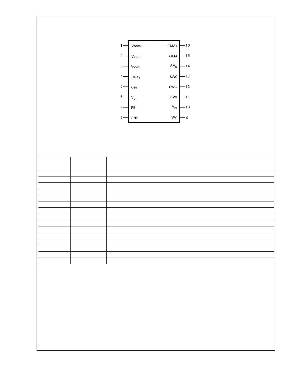
Connection Diagram
LM2702
Top View
TSSOP 16 package
= 125˚C, θJA= 120˚C/W (Note 1)
T
JMAX
Pin Description
Pin Name Function
1 Vcom+ Vcom Amplifier positive input.
2 Vcom− Vcom Amplifier negative input.
3 Vcom Vcom Amplifier output.
4 Delay Switch delay.
5 Css Soft start pin.
6V
C
7 FB Output Voltage Feedback input.
8 GND Ground.
9 SW NMOS power switch input.
10 V
IN
11 SWI PMOS switch input.
12 SWO PMOS switch output.
13 SWC PMOS switch control pin.
14 AV
IN
15 GMA Gamma buffer output.
16 GMA+ Gamma buffer input.
Boost Compensation Network Connection.
Main power input, step-up and switch circuitry.
Analog power input (buffers).
20051104
www.national.com 2
Pin Functions
Vcom+(Pin 1): Positive input terminal of Vcom amplifier.
Vcom−(Pin 2): Negative input terminal of Vcom amplifier.
Vcom(Pin 3): Output terminal of Vcom amplifier.
Delay(Pin 4): PMOS switch delay control pin. See Operation
section for setting the delay time.
The delay time begins when the output voltage of the DC/DC
switching regulator reaches 85% of its true output voltage.
This corresponds to a FB voltage of about 1.1V. The PMOS
switch is controlled with both the delay time and the switch
control pin, SWC. If no Cdelay capacitor is used, the PMOS
switch is controlled solely with the SWC pin.
Css(Pin 5): Softstart pin. Connect capacitor to Css pin and
AGND plane to slowly ramp inductor current on startup. See
Operation section for setting the softstart time.
(Pin 6): Compensation Network for Boost switching regu-
V
C
lator. Connect resistor/capacitor network between V
and AGND for boost switching regulator AC compensation.
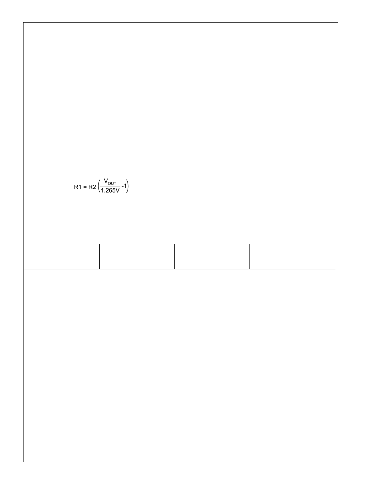
FB(Pin 7): Feedback pin. Set the output voltage by selecting
values of R1 and R2 using:
Connect the ground of the feedback network to the AGND
plane, which should be tied directly to the GND pin.
GND(Pin 8): Ground connect for LM2702. Connect all sensitive circuitry, ie. feedback resistors, softstart capacitor, de-
pin
C
lay capacitor, and compensation network to a dedicated
AGND plane which connects directly to this pin. Connect all
power ground components to a PGND plane which should
also connect directly to this pin. Please see Layout Considerations under the Operation section for more details on
layout suggestions.
SW(Pin 9): This is the drain of the internal NMOS power
switch. Minimize the metal trace area connected to this pin to
minimize EMI.
(Pin 10): Input Supply Pin. Bypass this pin with a capaci-
V
IN
tor as close to the device as possible. The capacitor should
connect between V
and GND.
IN
SWI(Pin 11): PMOS switch input. Source connection of
PMOS device.
SWO(Pin 12): PMOS switch output. Drain connection of
PMOS device.
SWC(Pin13): PMOS switch control pin. This pin creates an
AND function with the delay time after the output of the
switching regulator has reached 85% of its nominal value. To
ensure the PMOS switch is in the correct state, apply a
voltage above 1.5V to this pin to turn on the PMOS switch
and apply a voltage below 0.7V to turn off the PMOS switch.
(Pin 14): Supply pin for the Vcom opamp and the
AV
IN
Gamma buffer. Bypass this pin with a capacitor as close to
the device as possible, about 100nF. The capacitor should
connect between AV
and PGND.
IN
GMA(Pin 15): Gamma Buffer output pin.
GMA+(Pin 16): Gamma Buffer input pin.
LM2702
Ordering Information
Order Number Package Type NSC Package Drawing Supplied As
LM2702MT-ADJ TSSOP-16 MTC16 73 Units, Rail
LM2702MTX-ADJ TSSOP-16 MTC16 2500 Units, Tape and Reel
www.national.com3
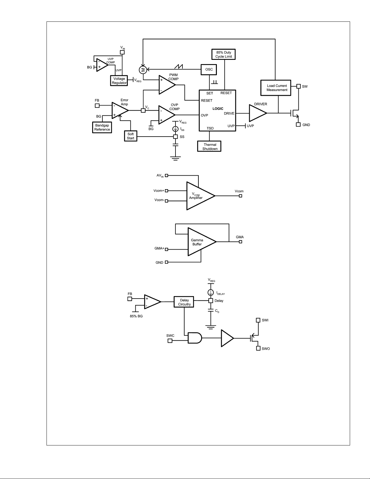
Block Diagrams
LM2702
20051103
20051151
20051157
www.national.com 4
Absolute Maximum Ratings (Note 2)
If Military/Aerospace specified devices are required,
please contact the National Semiconductor Sales Office/
Distributors for availability and specifications.
V
IN
-0.3V to 12V
SW Voltage -0.3V to 18V
FB Voltage -0.3V to 7V
V
Voltage 0.96V to 1.56V
C
Css Voltage -0.3V to 1.2V
SWC Voltage -0.3V to 12V
Supply Voltage, AV
IN
Amplifier/Buffer Input/Output
-0.3V to 12V
Rail-to-Rail
Voltage
Delay GND to 1.3V
SWI -0.3V to 30V
SWO -0.3V to 30V
ESD Ratings
(Notes 3, 4)
Human Body Model 2kV
Machine Model 200V
Operating Conditions
Operating Temperature −40˚C to +125˚C
Storage Temperature −65˚C to +150˚C
Supply Voltage, V
IN
SW Voltage 17.5V
Supply AV
IN
SWI 2.2V to 30V
2.2V to 12V
4V to 12V
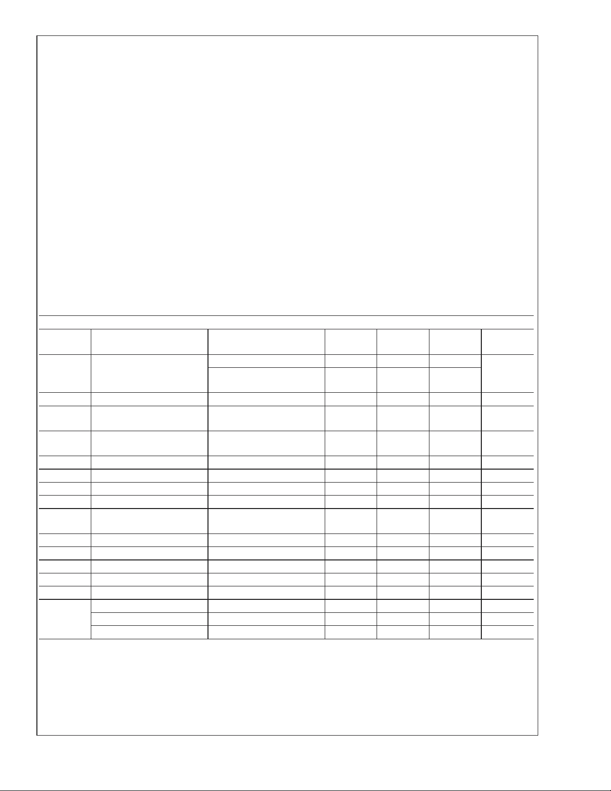
Electrical Characteristics
Specifications in standard type face are for TJ= 25˚C and those with boldface type apply over the full Operating Temperature Range (T
GAMMA
= 1nF.
C
= −40˚C to +125˚C). Unless otherwise specified, VIN=2.2V and AVIN= 8V, R
J
COM=RGAMMA
Switching Regulator
Symbol Parameter Conditions
I
Q
Quiescent Current Not Switching, FB = 2V 1.6 2.3
Switching, switch open, FB =
0.1V
V
FB
%V
/∆VINFeedback Voltage Line
FB
Feedback Voltage 1.239 1.265 1.291 V
Regulation
I
CL
Switch Current Limit
VIN= 2.7V
(Note 7)
R
I
V
I
T
DSON
B
IN
SS
SS
Switch R
(Note 8) VIN= 2.7V 200 mΩ
DSON
FB Pin Bias Current (Note 9) 60 500 nA
Input Voltage Range 2.2 12 V
Soft Start Current 5 12 15 µA
Internal Soft Start Ramp
Time
g
m
A
V
D
MAX
f
S
I
L
Error Amp Transconductance ∆I = 5µA 40 135 290 µmho
Error Amp Voltage Gain 135 V/V
Maximum Duty Cycle 78 85 %
Switching Frequency 480 600 720 kHz
Switch Leakage Current VSW= 18V 0.1 20 µA
Min
(Note 5)
1.4 2 2.6 A
Typ
(Note 6)
2.6 5.2
0.01 0.1 %/V
7 10 mS
UVP On Threshold 1.79 1.92 2.05 V
Off Threshold 1.69 1.82 1.95 V
Hysteresis 100 mV
Max
(Note 5)
=50Ω,C
COM
Units
mA
LM2702
=
www.national.com5
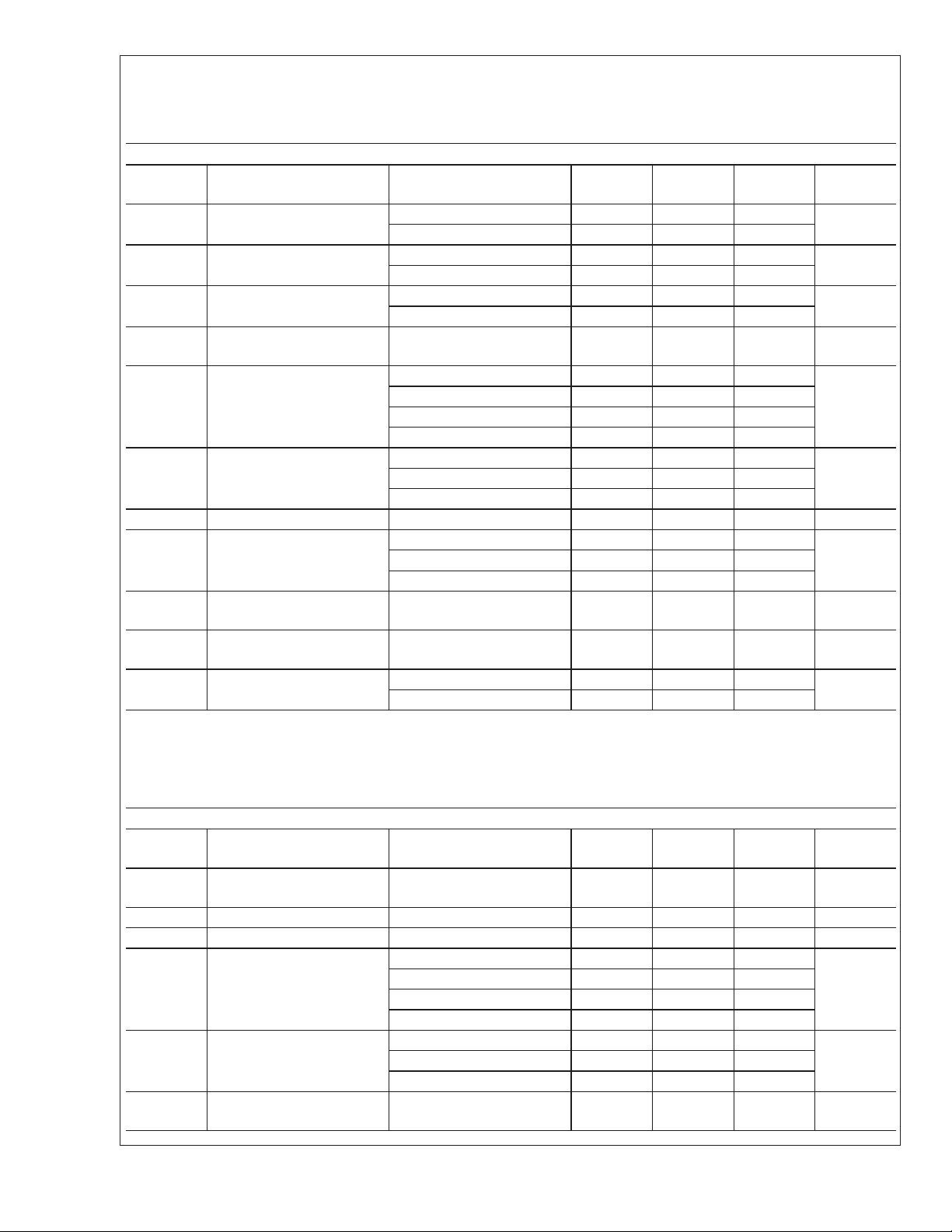
Electrical Characteristics
Specifications in standard type face are for TJ= 25˚C and those with boldface type apply over the full Operating Tempera-
LM2702
ture Range (T
GAMMA
= 1nF.
C
Vcom Amplifier
Symbol Parameter Conditions
V
OS
I
B
I
OS
CMVR Input Common-mode Voltage
V
Swing RL=10k, Vo min. 0.003 .02
OUT
A
VOL
AV
IN
CMRR Common Mode Rejection
PSRR Power Supply Rejection
Is+ Supply Current (Amplifier +
I
SC
= −40˚C to +125˚C). Unless otherwise specified, VIN=2.2V and AVIN= 8V, R
J
Min
(Note 5)
Input Offset Voltage (Note
10)
VCM= 1V 3.5 10
V
= 7.5V 3 10
CM
COM=RGAMMA
Typ
(Note 6)
=50Ω,C
Max
(Note 5)
Input Bias Current VCM= 1V 65 200
V
= 7.5V 190 300
CM
Input Offset Current VCM= 1V 45 130
V
= 7.5V 5 110
CM
Range
R
=10k, Vo max. 7.94 7.98
L
R
=2k, Vo min. 0.003 .02
L
R
=2k, Vo max. 7.9 7.95
L
08V
Large Signal Voltage Gain No Load, Vo = 2V to 7V 74.8 87.6
=10 kΩ,Vo=2Vto7V 66.8 75.1
L
R
=2 kΩ, Vo = 2V to 7V 55.8
L
Supply Voltage 412V
V
stepped from 0V to 1.1V 72 91.7
CM
Ratio
Ratio
Buffer)
stepped from 3V to 8V 80 105
CM
V
stepped from 0V to 8V 57 80.7
CM
V
= 0.5V, AVIN=4to12V
CM
Vo=AV
/2, No Load
IN
70 77 dB
2.2 4 mA
Output Short Circuit Current Source 40 50 70
Sink 40 50 60
COM
Units
mV
nA
nA
V
dBR
dBV
mA
=
Electrical Characteristics
Specifications in standard type face are for TJ= 25˚C and those with boldface type apply over the full Operating Temperature Range (T
GAMMA
= 1nF.
C
= −40˚C to +125˚C). Unless otherwise specified, VIN=2.2V and AVIN= 8V, R
J
Gamma Buffer
Symbol Parameter Conditions
V
OS
Input Offset Voltage (Note
Min
(Note 5)
Typ
(Note 6)
110mV
10)
I
B
V
GR
V
Swing RL=10k, Vo min. 0.05 0.075
OUT
A
VCL
PSRR Power Supply Rejection
www.national.com 6
Input Bias Current 170 300 nA
Gamma Input Voltage Range 08V
R
=10k, Vo max. 7.9 7.94
L
R
=2k, Vo min. 0.05 0.075
L
R
=2k, Vo max. 7.865 7.9
L
Voltage Gain No Load, Vo = 2V to 7V 0.995 0.999
=10 kΩ,Vo=2Vto7V 0.995 0.999
L
R
=2 kΩ,Vo=2Vto7V 0.993 0.998
L
AV
=4to12V
IN
Ratio
70 77 dB
COM=RGAMMA
=50Ω,C
Max
(Note 5)
COM
Units
V
V/VR
=
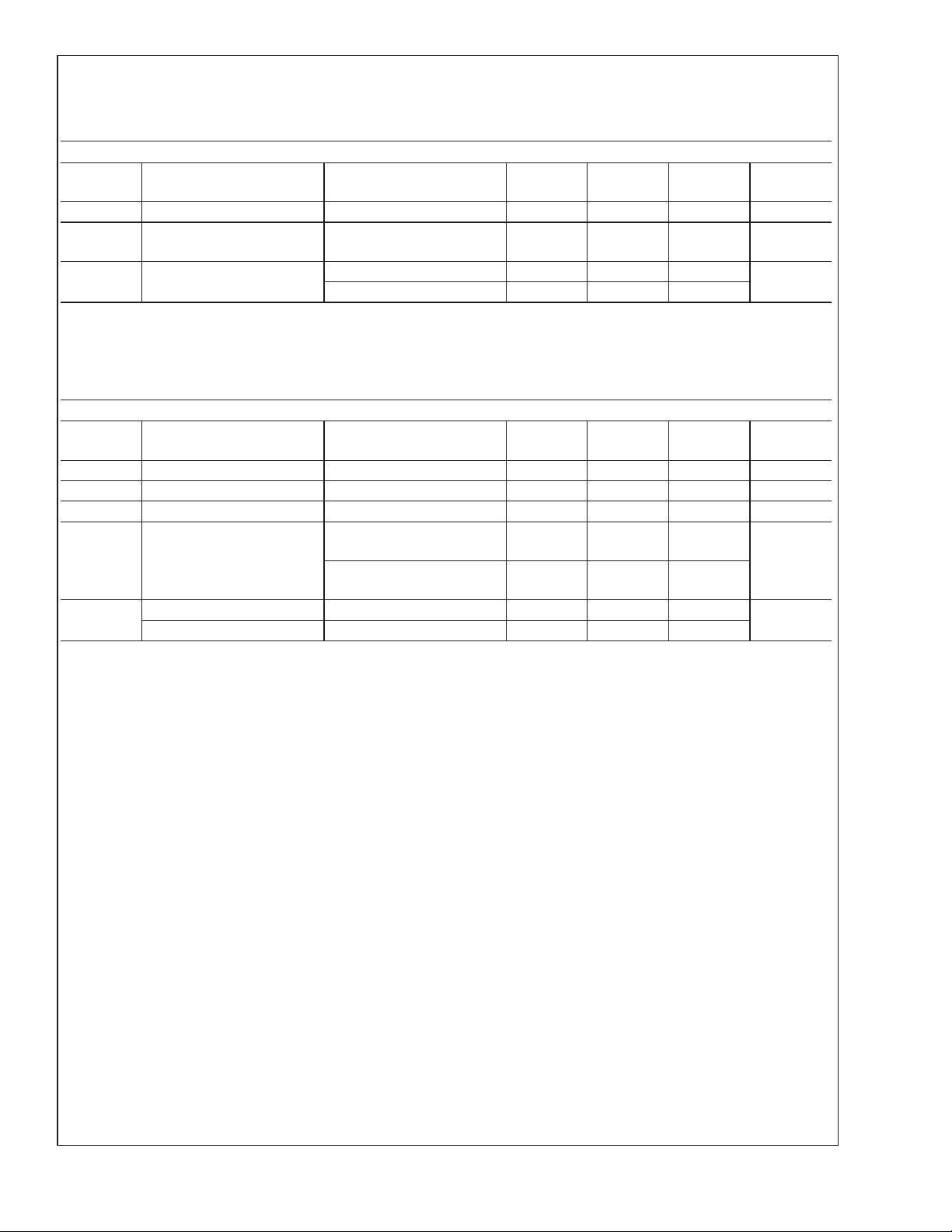
Electrical Characteristics (Continued)
Specifications in standard type face are for TJ= 25˚C and those with boldface type apply over the full Operating Temperature Range (T
GAMMA
= 1nF.
C
= −40˚C to +125˚C). Unless otherwise specified, VIN=2.2V and AVIN= 8V, R
J
COM=RGAMMA
=50Ω,C
Gamma Buffer
Symbol Parameter Conditions
AV
IN
Is+ Supply Current (Amplifier +
Supply Voltage 412V
Vo=AV
/2, No Load
IN
Buffer)
I
SC
Output Short Circuit Current Source 50 66 75
Min
(Note 5)
Typ
(Note 6)
Max
(Note 5)
2.2 4 mA
Units
Sink 40 56 65
Electrical Characteristics
Specifications in standard type face are for TJ= 25˚C and those with boldface type apply over the full Operating Temperature Range (T
GAMMA
= 1nF.
C
= −40˚C to +125˚C). Unless otherwise specified, VIN=2.2V and AVIN= 8V, R
J
COM=RGAMMA
PMOS Switch Logic Control
Symbol Parameter Conditions
I
DELAY
R
DSON
I
SWO
I
SWI
Delay Current 5.1 5.7 6.1 µA
PMOS Switch ON Resistance 7.3 20 Ω
PMOS Switch Current Switch ON 20 mA
PMOS Switch Input Current SWC = 0V, SWO Open, SWI
= 30V
SWC = 1.7V, SWO Open,
SWI = 30V
V
SWC
Switch ON 1.5 1.1
Min
(Note 5)
Typ
(Note 6)
32
118
Switch OFF 1.1 0.7
Note 1: The maximum allowable power dissipation is a function of the maximum junction temperature, TJ(MAX), the junction-to-ambient thermal resistance, θJA,
and the ambient temperature, T
at any ambient temperature is calculated using: P
temperature, and the regulator will go into thermal shutdown.
Note 2: Absolute maximum ratings are limits beyond which damage to the device may occur. Operating Ratings are conditions for which the device is intended to
be functional, but device parameter specifications may not be guaranteed. For guaranteed specifications and test conditions, see the Electrical Characteristics.
Note 3: The human body model is a 100 pF capacitor discharged through a 1.5kΩ resistor into each pin. The machine model is a 200pF capacitor discharged
directly into each pin.
Note 4: Vcom pin is rated for 1.5kV Human Body Model and 150V Machine Model.
Note 5: All limits guaranteed at room temperature (standard typeface) and at temperature extremes (bold typeface). All room temperature limits are 100%
production tested or guaranteed through statistical analysis. All limits at temperature extremes are guaranteed via correlation using standard Statistical Quality
Control (SQC) methods. All limits are used to calculate Average Outgoing Quality Level (AOQL).
Note 6: Typical numbers are at 25˚C and represent the most likely norm.
Note 7: Duty cycle affects current limit due to ramp generator. Current limit is at 0% duty cycle and will decrease with higher duty cycles. See Typical Performance
Characteristics for a graph of Power Switch Current Limit vs. V
Note 8: See the graph titled "R
Note 9: Bias current flows into FB pin.
Note 10: Refer to the graphs titled "Input Offset Voltage vs. Common Mode Voltage".
. See the Electrical Characteristics table for the thermal resistance of various layouts. The maximum allowable power dissipation
A
vs. VIN" for a more accurate value of the power switch R
DSON
(MAX) = (T
D
J(MAX)−TA
and Power Switch Current Limit vs. Temp.
IN
)/θJA. Exceeding the maximum allowable power dissipation will cause excessive die
.
DSON
Max
(Note 5)
=50Ω,C
Units
COM
mA
COM
µA
LM2702
=
=
V
www.national.com7
 Loading...