

NSC LM2700MT-ADJ Datasheet
October 2001
LM2700
600kHz/1.25MHz, 2.5A, Step-up PWM DC/DC Converter
General Description
The LM2700 is a step-up DC/DC converter with a 3.6A,
80mΩ internal switch and pin selectable operating frequency. With the ability to produce 500mA at 8V from a
single Lithium Ion battery, the LM2700 is an ideal part for
biasing LCD displays. The LM2700 can be operated at
switching frequencies of 600kHz and 1.25MHz allowing for
easy filtering and low noise. An external compensation pin
gives the user flexibility in setting frequency compensation,
which makes possible the use of small, low ESR ceramic
capacitors at the output. The LM2700 features continuous
switching at light loads and operates with a switching quiescent current of 2.0mA at 600kHz and 3.0mAat1.25MHz.The
LM2700 is available in a low profile 14-lead TSSOP package
or a 14-lead LLP package.
Features
n 3.6A, 0.08Ω, internal switch
n Operating input voltage range of 2.2V to 12V
n Input undervoltage protection
n Adjustable output voltage up to 17.5V
n 600kHz/1.25MHz pin selectable frequency operation
n Over temperature protection
n Small 14-Lead TSSOP or LLP package
Applications
n LCD Bias Supplies
n Handheld Devices
n Portable Applications
n GSM/CDMA Phones
n Digital Cameras
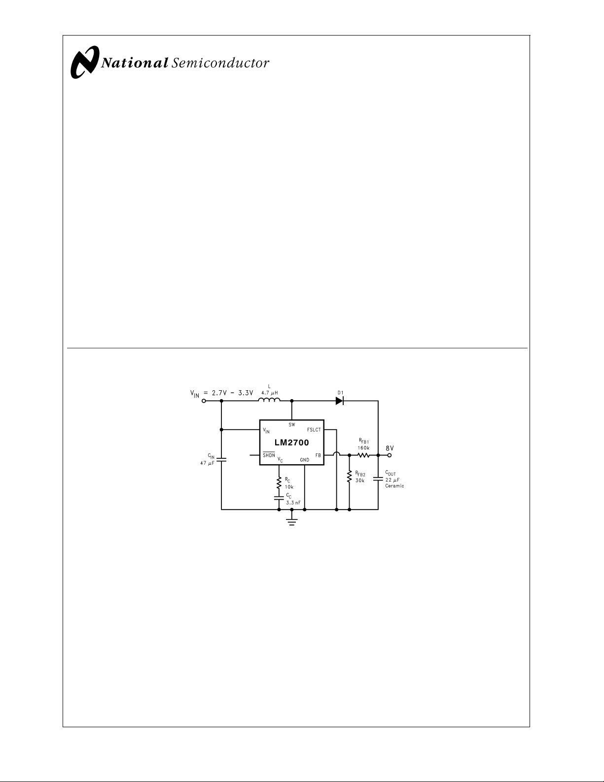
LM2700 600kHz/1.25MHz, 2.5A, Step-up PWM DC/DC Converter
Typical Application Circuit
600 kHz Operation
20012301
© 2001 National Semiconductor Corporation DS200123 www.national.com
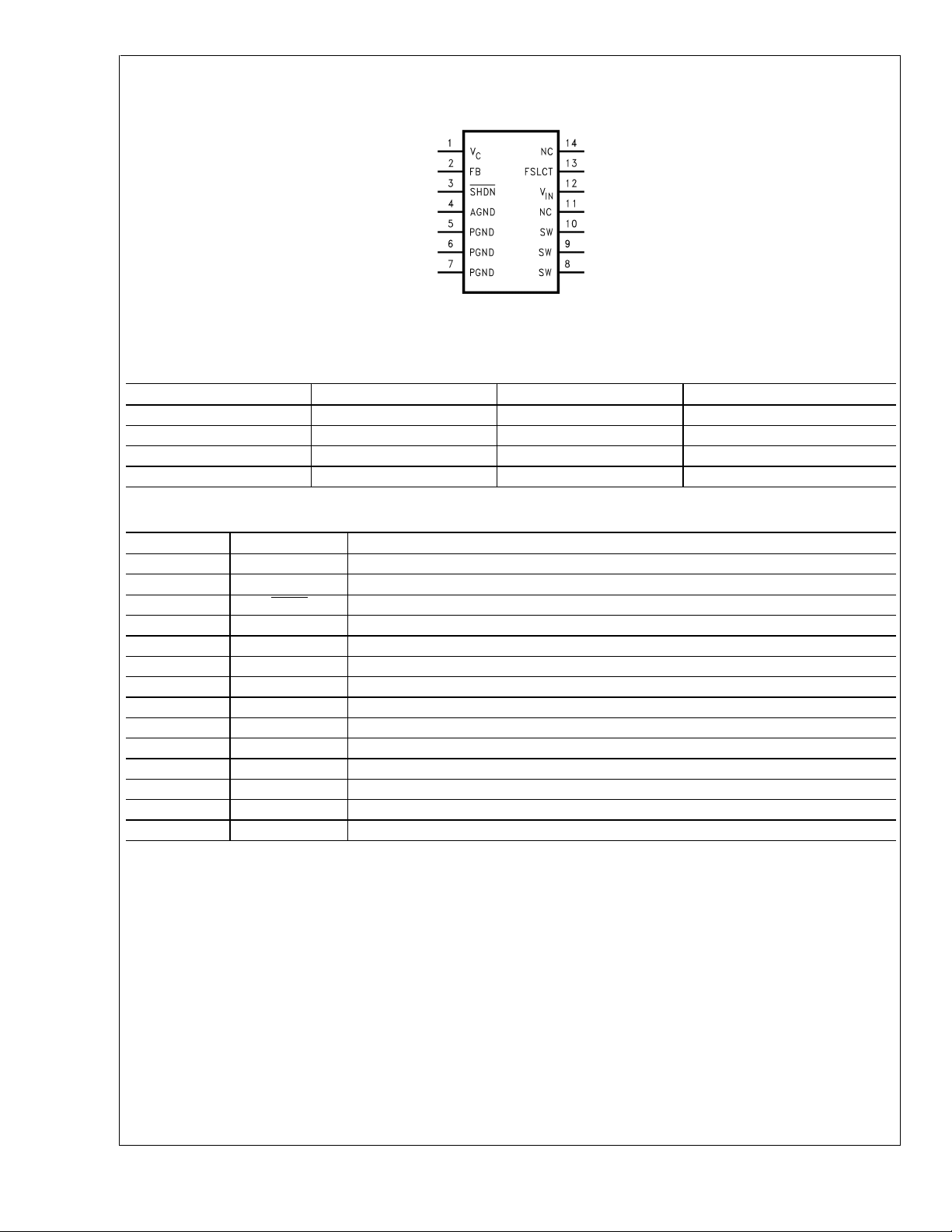
Connection Diagram
LM2700
Top View
14-Lead TSSOP or LLP
20012304
Ordering Information
Order Number Package Type NSC Package Drawing Supplied As
LM2700MT-ADJ TSSOP-14 MTC14 94 Units, Rail
LM2700MTX-ADJ TSSOP-14 MTC14 2500 Units, Tape and Reel
LM2700LD-ADJ LLP-14 LDA14A 1000 Units, Tape and Reel
LM2700LDX-ADJ LLP-14 LDA14A 4500 Units, Tape and Reel
Pin Description
Pin Name Function
1V
2 FB Output voltage feedback input.
3 SHDN
4 AGND Analog ground.
5 PGND Power ground. PGND pins must be connected together directly at the part.
6 PGND Power ground. PGND pins must be connected together directly at the part.
7 PGND Power ground. PGND pins must be connected together directly at the part.
8 SW Power switch input. Switch connected between SW pins and PGND pins.
9 SW Power switch input. Switch connected between SW pins and PGND pins.
10 SW Power switch input. Switch connected between SW pins and PGND pins.
11 NC Pin not connected internally.
12 V
13 FSLCT Switching frequency select input. V
14 NC Connect to ground.
C
IN
Compensation network connection. Connected to the output of the voltage error amplifier.
Shutdown control input, active low.
Analog power input.
= 1.25MHz. Ground = 600kHz.
IN
www.national.com 2
Block Diagram
LM2700
Detailed Description
The LM2700 utilizes a PWM control scheme to regulate the
output voltage over all load conditions. The operation can
best be understood referring to the block diagram and
1
of the
Operation
oscillator sets the driver logic and turns on the NMOS power
device conducting current through the inductor, cycle 1 of
Figure 1
controls the peak inductor current. The V
crease with larger loads and decrease with smaller. This
voltage is compared with the summation of the SW voltage
and the ramp compensation. The ramp compensation is
used in PWM architectures to eliminate the sub-harmonic
oscillations that occur during duty cycles greater than 50%.
Once the summation of the ramp compensation and switch
voltage equals the V
(a). During this cycle, the voltage at the VCpin
section. At the start of each cycle, the
voltage will in-
C
voltage, the PWM comparator resets
C
Figure
20012303
the driver logic turning off the NMOS power device. The
inductor current then flows through the schottky diode to the
load and output capacitor, cycle 2 of
power device is then set by the oscillator at the end of the
period and current flows through the inductor once again.
The LM2700 has dedicated protection circuitry running during normal operation to protect the IC. The Thermal Shutdown circuitry turns off the NMOS power device when the
die temperature reaches excessive levels. The UVP comparator protects the NMOS power device during supply
power startup and shutdown to prevent operation at voltages
less than the minimum input voltage. The OVPcomparator is
used to prevent the output voltage from rising at no loads
allowing full PWM operation over all load conditions. The
LM2700 also features a shutdown mode decreasing the
supply current to 5µA.
Figure 1
(b). The NMOS
www.national.com3
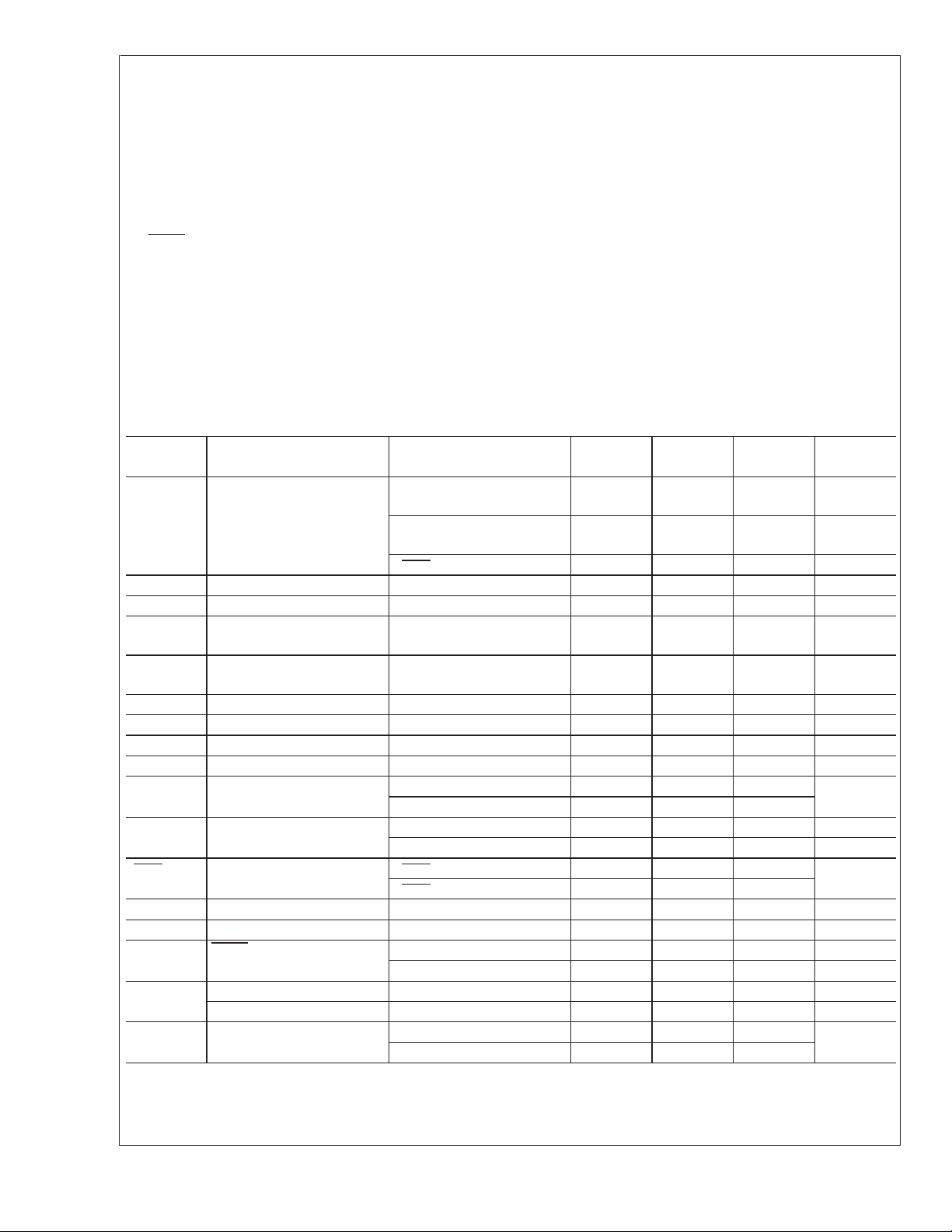
Absolute Maximum Ratings (Note 2)
If Military/Aerospace specified devices are required,
LM2700
please contact the National Semiconductor Sales Office/
Distributors for availability and specifications.
V
IN
SW Voltage 18V
12V
Infrared (15 sec.) 220˚C
ESD Susceptibility (Note 4)
Human Body Model 2kV
Machine Model 200V
Operating Conditions
FB Voltage 7V
V
Voltage 0.965V ≤ VC≤ 1.565V
C
SHDN Voltage (Note 1)
7V
FSLCT (Note 1) 12V
Maximum Junction Temperature 150˚C
Power Dissipation(Note 3) Internally Limited
Lead Temperature 300˚C
Operating Junction
Temperature Range
(Note 5) −40˚C to +125˚C
Storage Temperature −65˚C to +150˚C
Supply Voltage 2.2V to 12V
SW Voltage 17.5V
Vapor Phase (60 sec.) 215˚C
Electrical Characteristics
Specifications in standard type face are for TJ= 25˚C and those with boldface type apply over the full Operating Temperature Range (T
Symbol Parameter Conditions
I
Q
V
FB
I
(Note 7) Switch Current Limit VIN= 2.7V (Note 8) 2.55 3.6 4.3 A
CL
%V
/∆VINFeedback Voltage Line
FB
I
B
V
IN
g
m
A
V
D
MAX
D
MIN
f
S
I
SHDN
I
L
R
DSON
Th
SHDN
UVP On Threshold 1.95 2.05 2.2 V
θ
JA
Note 1: This voltage should never exceed VIN.
Note 2: Absolute maximum ratings are limits beyond which damage to the device may occur. Operating Ratings are conditions for which the device is intended to
be functional, but device parameter specifications may not be guaranteed. For guaranteed specifications and test conditions, see the Electrical Characteristics.
= −40˚C to +125˚C) Unless otherwise specified. VIN=2.2V and IL= 0A, unless otherwise specified.
J
Quiescent Current FB = 2.2V (Not Switching)
FSLCT = 0V
FB = 2.2V (Not Switching)
FSLCT = V
V
SHDN
IN
=0V 5 20 µA
Min
(Note 5)
Typ
(Note 6)
Max
(Note 5)
1.2 2 mA
1.3 2 mA
Feedback Voltage 1.2285 1.26 1.2915 V
2.2V ≤ VIN≤ 12.0V 0.02 0.07 %/V
Regulation
FB Pin Bias Current
0.5 40
(Note 9)
Input Voltage Range 2.2 12 V
Error Amp Transconductance ∆I = 5µA 40 155 290 µmho
Error Amp Voltage Gain 135 V/V
Maximum Duty Cycle FSLCT = Ground 78 85 %
Minimum Duty Cycle FSLCT = Ground 15
FSLCT = V
IN
30
Switching Frequency FSLCT = Ground 480 600 720 kHz
Shutdown Pin Current V
FSLCT = V
SHDN
V
SHDN
IN
=V
IN
=0V −0.5 −1
1 1.25 1.5 MHz
0.008 1
Switch Leakage Current VSW= 18V 0.02 20 µA
Switch R
(Note 10) VIN= 2.7V, ISW=2A 80 150 mΩ
DSON
SHDN Threshold Output High 0.9 0.6 V
Output Low 0.6 0.3 V
Off Threshold 1.85 1.95 2.1 V
Thermal Resistance
(Note 11)
TSSOP, package only 150
LLP, package only 45
Units
nA
%
µA
˚C/W
www.national.com 4
Electrical Characteristics (Continued)
Note 3: The maximum allowable power dissipation is a function of the maximum junction temperature, TJ(MAX), the junction-to-ambient thermal resistance, θJA,
and the ambient temperature, T
temperature is calculatedusing:P
regulator will go into thermal shutdown.
Note 4: The human body model is a 100 pF capacitor discharged through a 1.5kΩ resistor into each pin. The machine model is a 200pF capacitor discharged
directly into each pin.
Note 5: All limits guaranteed at room temperature (standard typeface) and at temperature extremes (bold typeface). All room temperature limits are 100% tested
or guaranteed through statistical analysis.All limits at temperature extremes are guaranteed via correlation using standard Statistical Quality Control (SQC) methods.
All limits are used to calculate Average Outgoing Quality Level (AOQL).
Note 6: Typical numbers are at 25˚C and represent the most likely norm.
Note 7: Duty cycle affects current limit due to ramp generator.
Note 8: Current limit at 0% duty cycle. See TYPICAL PERFORMANCE section for Switch Current Limit vs. V
Note 9: Bias current flows into FB pin.
Note 10: Does not include the bond wires. Measured directly at the die.
Note 11: Refer to National’s packaging website for more detailed thermal information and mounting techniques for the LLP and TSSOP packages.
. See the Electrical Characteristics table for the thermal resistance. The maximum allowable power dissipation at any ambient
A
(MAX) = (T
D
J(MAX)−TA
)/θJA. Exceeding the maximum allowable power dissipation will cause excessive die temperature, and the
IN
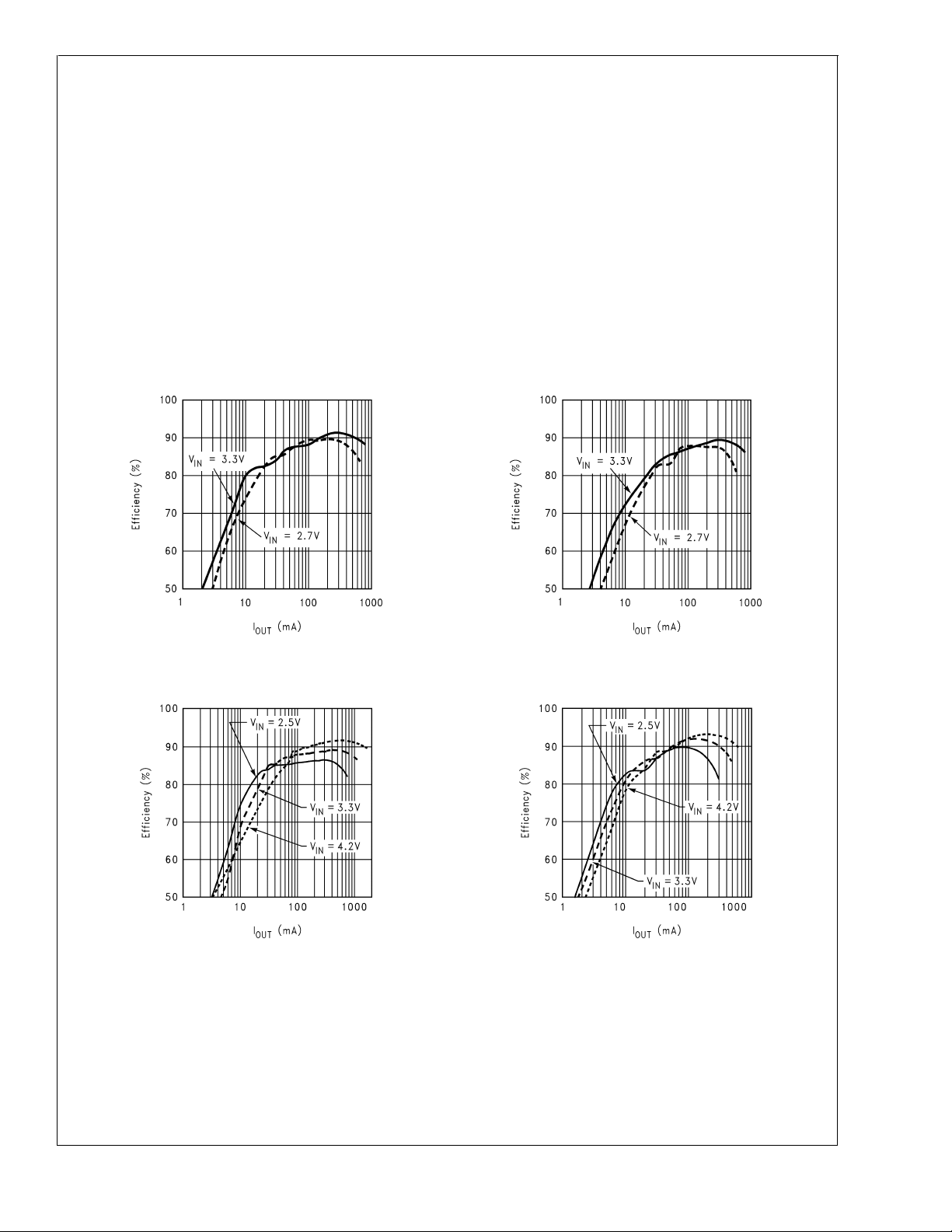
Typical Performance Characteristics
Efficiency vs. Load Current
(V
= 8V, fS= 600 kHz)
OUT
Efficiency vs. Load Current
(V
= 8V, fS= 1.25 MHz)
OUT
LM2700
Efficiency vs. Load Current
(V
= 5V, fS= 600 kHz)
OUT
20012326 20012325
Efficiency vs. Load Current
(V
= 12V, fS= 600 kHz)
OUT
20012334 20012335
www.national.com5
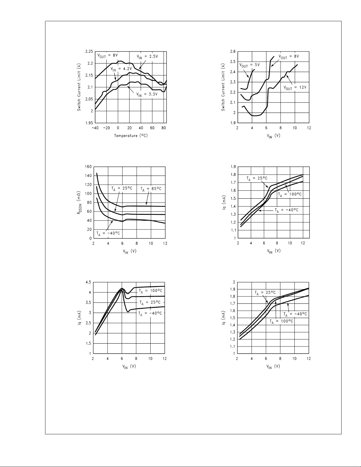
Typical Performance Characteristics (Continued)
LM2700
Switch Current Limit vs. Temperature Switch Current Limit vs. V
20012320
R
vs. V
DSON
(ISW= 2A)
IN
(600 kHz, not switching)
I
Q
vs. V
IN
IN
20012322
IQvs. V
IN
(600 kHz, switching)
20012327
I
Q
vs. V
IN
20012328
(1.25 MHz, not switching)
20012329 20012321
www.national.com 6
 Loading...