

NSC LM26LV, LM26LVCISD-XPE Datasheet
July 2007
LM26LV
1.6 V, LLP-6 Factory Preset Temperature Switch and
Temperature Sensor
General Description
The LM26LV is a low-voltage, precision, dual-output, lowpower temperature switch and temperature sensor. The temperature trip point (T
TRIP
) can be preset at the factory to any
temperature in the range of 0°C to 150°C in 1°C increments.
Built-in temperature hysteresis (T
HYST
) keeps the output sta-
ble in an environment of temperature instability.
In normal operation the LM26LV temperature switch outputs
assert when the die temperature exceeds T
TRIP
. The temperature switch outputs will reset when the temperature falls
below a temperature equal to (T
TRIP
− T
HYST
). The
OVERTEMP digital output, is active-high with a push-pull
structure, while the OVERTEMP
digital output, is active-low
with an open-drain structure.
An analog output, V
TEMP
, delivers an analog output voltage
which is inversely proportional to the measured temperature.
Driving the TRIP TEST input high: (1) causes the digital out-
puts to be asserted for in-situ verification and, (2) causes the
threshold voltage to appear at the V
TEMP
output pin, which
could be used to verify the temperature trip point.
The LM26LV's low minimum supply voltage makes it ideal for
1.8 Volt system designs. Its wide operating range, low supply
current , and excellent accuracy provide a temperature switch
solution for a wide range of commercial and industrial applications.
Applications
■
Cell phones
■
Wireless Transceivers
■
Digital Cameras
■
Personal Digital Assistants (PDA's)
■
Battery Management
■
Automotive
■
Disk Drives
■
Games
■
Appliances
Features
■
Low 1.6V operation
■
Low quiescent current
■
Push-pull and open-drain temperature switch outputs
■
Wide trip point range of 0°C to 150°C
■
Very linear analog V
TEMP
temperature sensor output
■
V
TEMP
output short-circuit protected
■
Accurate over −50°C to 150°C temperature range
■
2.2 mm by 2.5 mm (typ) LLP-6 package
■
Excellent power supply noise rejection
Key Specifications
■ Supply Voltage
1.6V to 5.5V
■ Supply Current
8 μA (typ)
■ Accuracy, Trip Point
Temperature
0°C to 150°C ±2.2°C
■ Accuracy, V
TEMP
0°C to 150°C ±2.3°C
0°C to 120°C ±2.2°C
−50°C to 0°C ±1.7°C
■ V
TEMP
Output Drive
±100 μA
■ Operating Temperature −50°C to 150°C
■ Hysteresis Temperature 4.5°C to 5.5°C
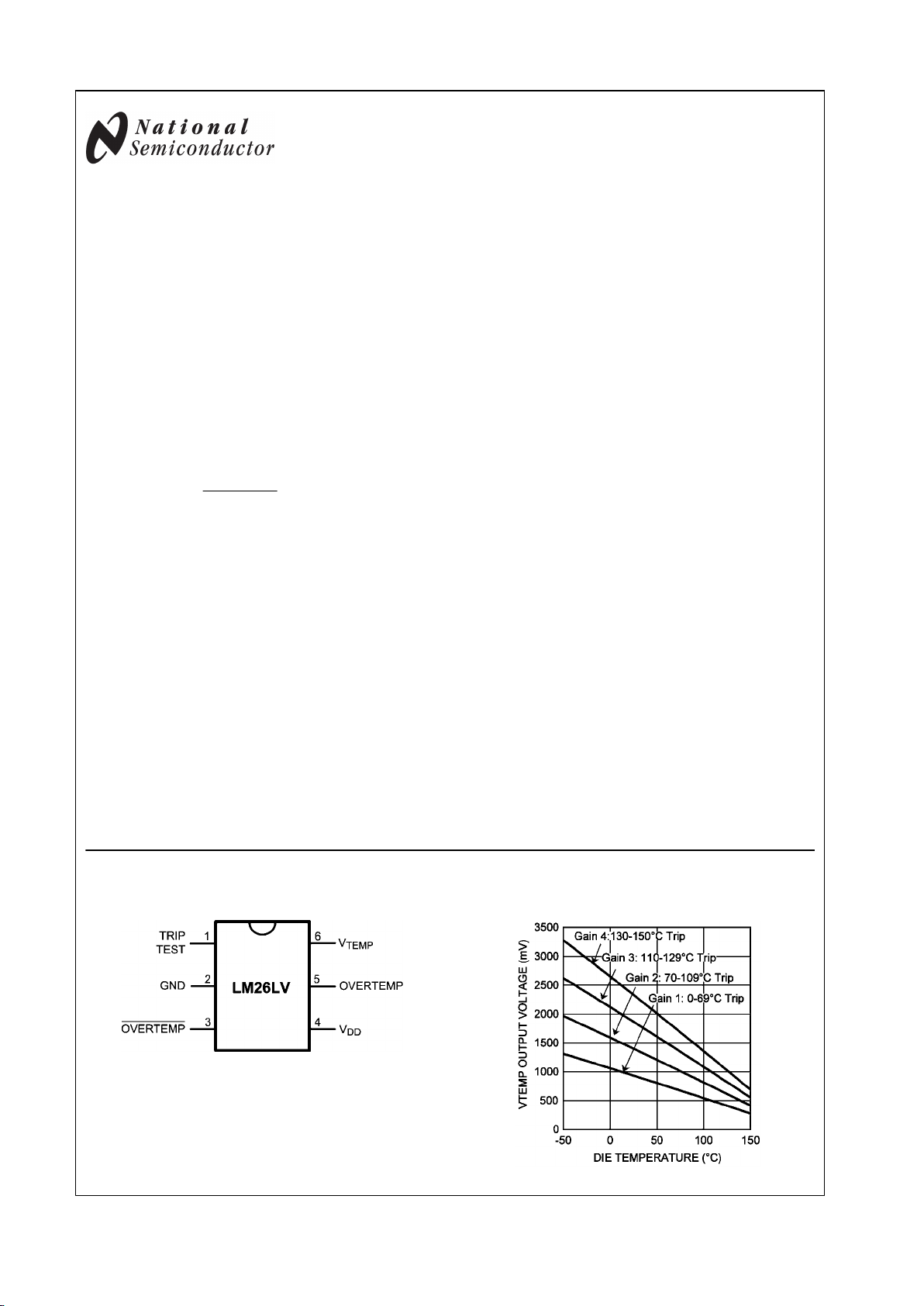
Connection Diagram
LLP-6
20204701
Top View
See NS Package Number SDB06A
Typical Transfer Characteristic
V
TEMP
Analog Voltage vs Die Temperature
20204724
© 2007 National Semiconductor Corporation 202047 www.national.com
LM26LV 1.6 V, LLP-6 Factory Preset Temperature Switch and Temperature Sensor
Block Diagram
20204703
Pin Descriptions
Pin
No.
Name Type Equivalent Circuit Description
1
TRIP
TEST
Digital
Input
TRIP TEST pin. Active High input.
If TRIP TEST = 0 (Default) then:
V
TEMP
= VTS, Temperature Sensor Output Voltage
If TRIP TEST = 1 then:
OVERTEMP and OVERTEMP outputs are asserted and
V
TEMP
= V
TRIP
, Temperature Trip Voltage.
This pin may be left open if not used.
5 OVERTEMP
Digital
Output
Over Temperature Switch output
Active High, Push-Pull
Asserted when the measured temperature exceeds the Trip
Point Temperature or if TRIP TEST = 1
This pin may be left open if not used.
3 OVERTEMP
Digital
Output
Over Temperature Switch output
Active Low, Open-drain (See Section 2.1 regarding required pullup resistor.)
Asserted when the measured temperature exceeds the Trip
Point Temperature or if TRIP TEST = 1
This pin may be left open if not used.
6
V
TEMP
Analog
Output
V
TEMP
Analog Voltage Output
If TRIP TEST = 0 then
V
TEMP
= VTS, Temperature Sensor Output Voltage
If TRIP TEST = 1 then
V
TEMP
= V
TRIP
, Temperature Trip Voltage
This pin may be left open if not used.
4
V
DD
Power
Positive Supply Voltage
2 GND Ground Power Supply Ground
www.national.com 2
LM26LV
Typical Application
20204702
Ordering Information
Order Number
Temperature Trip
Point, °C
NS Package
Number
Top Mark Transport Media
LM26LVCISD-XPE 105°C SDB06A XPE 1000 Units on Tape and Reel
LM26LVCISDX-XPE 105°C SDB06A XPE 4500 Units on Tape and Reel
3 www.national.com
LM26LV
Absolute Maximum Ratings (Note 1)
Supply Voltage −0.2V to +6.0V
Voltage at OVERTEMP pin −0.2V to +6.0V
Voltage at OVERTEMP and
V
TEMP
pins −0.2V to (VDD + 0.5V)
TRIP TEST Input Voltage −0.2V to (VDD + 0.5V)
Output Current, any output pin ±7 mA
Input Current at any pin (Note 2) 5 mA
Storage Temperature −65°C to +150°C
Maximum Junction Temperature
T
J(MAX)
+155°C
ESD Susceptibility (Note 3) :
Human Body Model 2500V
Machine Model 250V
Charged Device Model 1000V
Soldering process must comply with National's
Reflow Temperature Profile specifications. Refer to
www.national.com/packaging. (Note 4)
Operating Ratings (Note 1)
Specified Temperature Range:
T
MIN
≤ TA ≤ T
MAX
LM26LV
−50°C ≤ TA ≤ +150°C
Supply Voltage Range (VDD)
+1.6 V to +5.5 V
Thermal Resistance (θJA) (Note 5)
LLP-6 (Package SDB06A) 152 °C/W
Accuracy Characteristics
Trip Point Accuracy
Parameter Conditions
Limits
(Note 7)
Units
(Limit)
Trip Point Accuracy (Note 8) 0 − 150°C
VDD = 5.0 V
±2.2 °C (max)
V
TEMP
Analog Temperature Sensor Output Accuracy
There are four gains corresponding to each of the four Temperature Trip Point Ranges. Gain 1 is the sensor gain used for Temperature Trip Point 0 - 69°C. Likewise Gain 2 is for Trip Points 70 - 109 °C; Gain 3 for 110 - 129 °C; and Gain 4 for 130 - 150 °C.
These limits do not include DC load regulation. These stated accuracy limits are with reference to the values in the LM26LV
Conversion Table.
Parameter Conditions
Limits
(Note 7)
Units
(Limit)
V
TEMP
Temperature
Accuracy
(Note 8)
Gain 1: for Trip Point
Range 0 - 69°C
TA = 20°C to 40°C VDD = 1.6 to 5.5 V
±1.8
°C (max)
TA = 0°C to 70°C VDD = 1.6 to 5.5 V
±2.0
TA = 0°C to 90°C VDD = 1.6 to 5.5 V
±2.1
TA = 0°C to 120°C VDD = 1.6 to 5.5 V
±2.2
TA = 0°C to 150°C VDD = 1.6 to 5.5 V
±2.3
TA = −50°C to 0°C VDD = 1.7 to 5.5 V
±1.7
Gain 2: for Trip Point
Range 70 - 109°C
TA = 20°C to 40°C VDD = 1.8 to 5.5 V
±1.8
°C (max)
TA = 0°C to 70°C VDD = 1.9 to 5.5 V
±2.0
TA = 0°C to 90°C VDD = 1.9 to 5.5 V
±2.1
TA = 0°C to 120°C VDD = 1.9 to 5.5 V
±2.2
TA = 0°C to 150°C VDD = 1.9 to 5.5 V
±2.3
TA = −50°C to 0°C VDD = 2.3 to 5.5 V
±1.7
Gain 3: for Trip Point
Range 110 - 129°C
TA = 20°C to 40°C VDD = 2.3 to 5.5 V
±1.8
°C (max)
TA = 0°C to 70°C VDD = 2.5 to 5.5 V
±2.0
TA = 0°C to 90°C VDD = 2.5 to 5.5 V
±2.1
TA = 0°C to 120°C VDD = 2.5 to 5.5 V
±2.2
TA = 0°C to 150°C VDD = 2.5 to 5.5 V
±2.3
TA = −50°C to 0°C VDD = 3.0 to 5.5 V
±1.7
Gain 4: for Trip Point
Range 130 - 150°C
TA = 20°C to 40°C VDD = 2.7 to 5.5 V
±1.8
°C (max)
TA = 0°C to 70°C VDD = 3.0 to 5.5 V
±2.0
TA = 0°C to 90°C VDD = 3.0 to 5.5 V
±2.1
TA = 0°C to 120°C VDD = 3.0 to 5.5 V
±2.2
TA = 0°C to 150°C VDD = 3.0 to 5.5 V
±2.3
TA = −50°C to 0°C VDD = 3.6 to 5.5 V
±1.7
www.national.com 4
LM26LV
Electrical Characteristics
Unless otherwise noted, these specifications apply for +VDD = +1.6V to +5.5V. Boldface limits apply for TA = TJ = T
MIN
to
T
MAX
; all other limits TA = TJ = 25°C.
Symbol Parameter Conditions Typical
(Note 6)
Limits
(Note 7)
Units
(Limit)
GENERAL SPECIFICATIONS
I
S
Quiescent Power Supply
Current
8 16
μA (max)
Hysteresis
5
5.5 °C (max)
4.5 °C (Min)
OVERTEMP DIGITAL OUTPUT ACTIVE HIGH, PUSH-PULL
V
OH
Logic "1" Output Voltage
VDD ≥ 1.6V Source ≤ 340 μA
VDD − 0.2V
V (min)
VDD ≥ 2.0V Source ≤ 498 μA
VDD ≥ 3.3V Source ≤ 780 μA
VDD ≥ 1.6V Source ≤ 600 μA
VDD − 0.45V
V (min)
VDD ≥ 2.0V Source ≤ 980 μA
VDD ≥ 3.3V Source ≤ 1.6 mA
BOTH OVERTEMP and OVERTEMP DIGITAL OUTPUTS
V
OL
Logic "0" Output Voltage
VDD ≥ 1.6V Sink ≤ 385 μA
0.2
V (max)
VDD ≥ 2.0V Sink ≤ 500 μA
VDD ≥ 3.3V Sink ≤ 730 μA
VDD ≥ 1.6V Sink ≤ 690 μA
0.45
VDD ≥ 2.0V Sink ≤ 1.05 mA
VDD ≥ 3.3V Sink ≤ 1.62 mA
OVERTEMP DIGITAL OUTPUT ACTIVE LOW, OPEN DRAIN
I
OH
Logic "1" Output Leakage
Current (Note 12)
TA = 30 °C
0.001
1
μA (max)
TA = 150 °C
0.025
V
TEMP
ANALOG TEMPERATURE SENSOR OUTPUT
V
TEMP
Sensor Gain
Gain 1: If Trip Point = 0 - 69°C −5.1 mV/°C
Gain 2: If Trip Point = 70 - 109°C −7.7 mV/°C
Gain 3: If Trip Point = 110 - 129°C −10.3 mV/°C
Gain 4: If Trip Point = 130 - 150°C −12.8 mV/°C
V
TEMP
Load Regulation
(Note 10)
Source ≤ 90 μA, (VDD − V
TEMP
) ≥ 200 mV
−0.1 −1 mV (max)
Sink ≤ 100 μA, V
TEMP
≥ 260 mV
0.1 1 mV (max)
Source or Sink = 100 μA
1 Ohm
VDD Supply- to-V
TEMP
DC Line Regulation
(Note 13)
VDD = +1.6V to +5.5V
0.29 mV
74
μV/V
−82 dB
C
L
V
TEMP
Output Load
Capacitance
Without series resistor. See Section 4.2 1100
pF (max)
TRIP TEST DIGITAL INPUT
V
IH
Logic "1" Threshold Voltage
VDD− 0.5
V (min)
V
IL
Logic "0" Threshold Voltage
0.5 V (max)
I
IH
Logic "1" Input Current
1.5 2.5
μA (max)
I
IL
Logic "0" Input Current
(Note 12)
0.001 1
μA (max)
5 www.national.com
LM26LV
Symbol Parameter Conditions Typical
(Note 6)
Limits
(Note 7)
Units
(Limit)
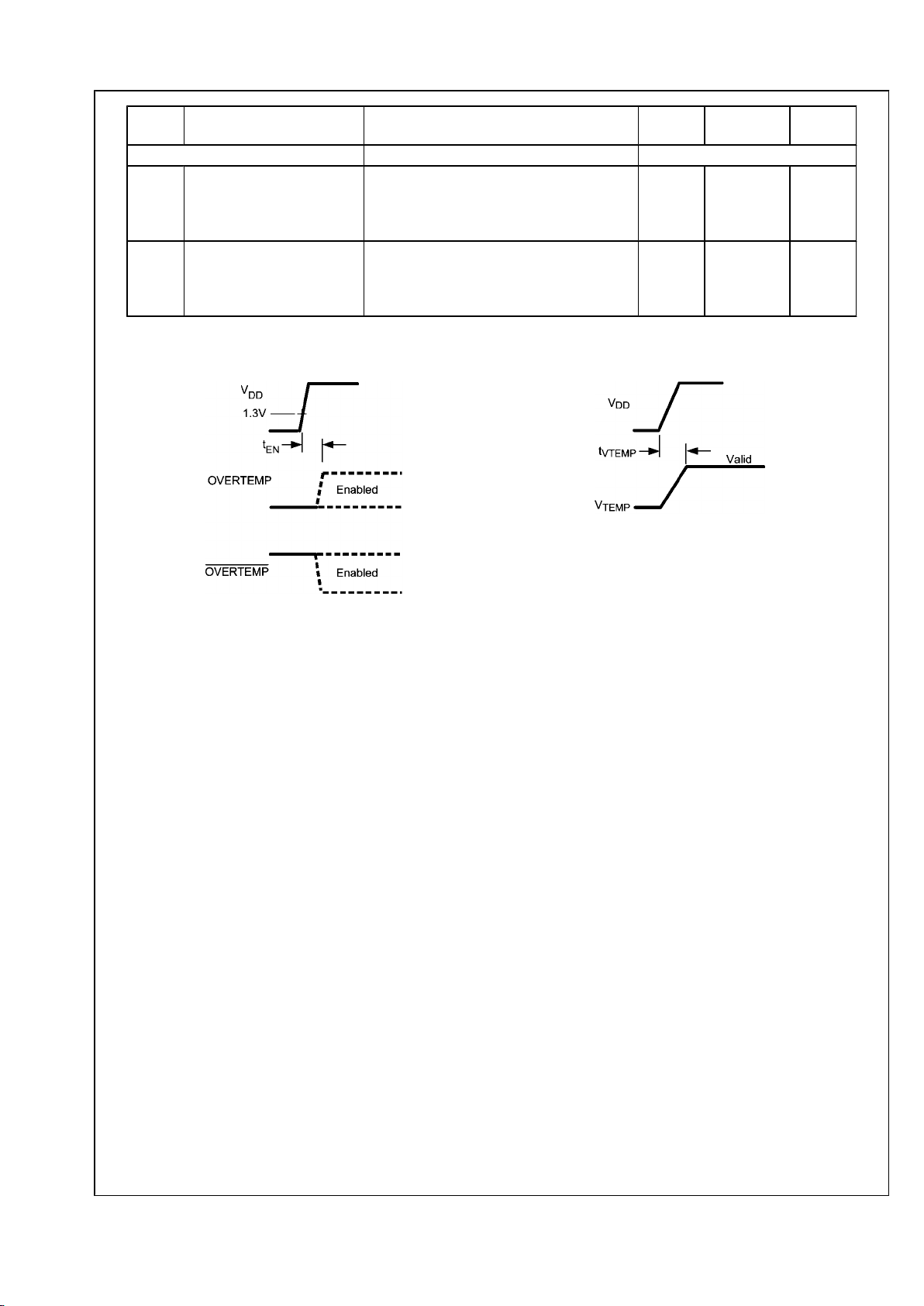
TIMING
t
EN
Time from Power On to Digital
Output Enabled. See
definition below.
(Note 11).
1.1 10 ms (max)
t
V
TEMP
Time from Power On to
Analog Temperature Valid.
See definition below.
(Note 11)
0.9 10 ms (max)
Definitions of tEN and t
V
TEMP
20204750
20204751
Notes
Note 1: Absolute Maximum Ratings indicate limits beyond which damage to the device may occur. Operating Ratings indicate conditions for which the device is
functional, but do not guarantee specific performance limits. For guaranteed specifications and test conditions, see the Electrical Characteristics. The guaranteed
specifications apply only for the test conditions listed. Some performance characteristics may degrade when the device is not operated under the listed test
conditions.
Note 2: When the input voltage (VI) at any pin exceeds power supplies (VI < GND or VI > VDD), the current at that pin should be limited to 5 mA.
Note 3: The Human Body Model (HBM) is a 100 pF capacitor charged to the specified voltage then discharged through a 1.5 kΩ resistor into each pin. The
Machine Model (MM) is a 200 pF capacitor charged to the specified voltage then discharged directly into each pin. The Charged Device Model (CDM) is a specified
circuit characterizing an ESD event that occurs when a device acquires charge through some triboelectric (frictional) or electrostatic induction processes and then
abruptly touches a grounded object or surface.
Note 4: Reflow temperature profiles are different for lead-free and non-lead-free packages.
Note 5: The junction to ambient temperature resistance (θJA) is specified without a heat sink in still air.
Note 6: Typicals are at TJ = TA = 25°C and represent most likely parametric norm.
Note 7: Limits are guaranteed to National's AOQL (Average Outgoing Quality Level).
Note 8: Accuracy is defined as the error between the measured and reference output voltages, tabulated in the Conversion Table at the specified conditions of
supply gain setting, voltage, and temperature (expressed in °C). Accuracy limits include line regulation within the specified conditions. Accuracy limits do not
include load regulation; they assume no DC load.
Note 9: Changes in output due to self heating can be computed by multiplying the internal dissipation by the temperature resistance.
Note 10: Source currents are flowing out of the LM26LV. Sink currents are flowing into the LM26LV.
Note 11: Guaranteed by design.
Note 12: The 1 µA limit is based on a testing limitation and does not reflect the actual performance of the part. Expect to see a doubling of the current for every
15°C increase in temperature. For example, the 1 nA typical current at 25°C would increase to 16 nA at 85°C.
Note 13: Line regulation (DC) is calculated by subtracting the output voltage at the highest supply voltage from the output voltage at the lowest supply voltage.
The typical DC line regulation specification does not include the output voltage shift discussed in Section 4.3.
Note 14: The curves shown represent typical performance under worst-case conditions. Performance improves with larger overhead (VDD − V
TEMP
), larger VDD,
and lower temperatures.
Note 15: The curves shown represent typical performance under worst-case conditions. Performance improves with larger V
TEMP
, larger VDD and lower
temperatures.
www.national.com 6
LM26LV
 Loading...