

NSC LM2698MM-ADJ, LM2698EVAL, LM2698MMX-ADJ Datasheet
LM2698
SIMPLE SWITCHER
®
1.35A Boost Regulator
General Description
The LM2698 is a general purpose PWM boost converter.
The 1.9A, 18V, 0.2ohm internal switch enables the LM2698
to provide efficient power conversion to outputs ranging from
2.2V to 17V.Itcanoperate with input voltages as low as 2.2V
and as high as 12V. Current-mode architecture provides
superior line and load regulation and simple frequency compensation over the device’s 2.2V to 12V input voltagerange.
The LM2698 sets the standard in power density and is
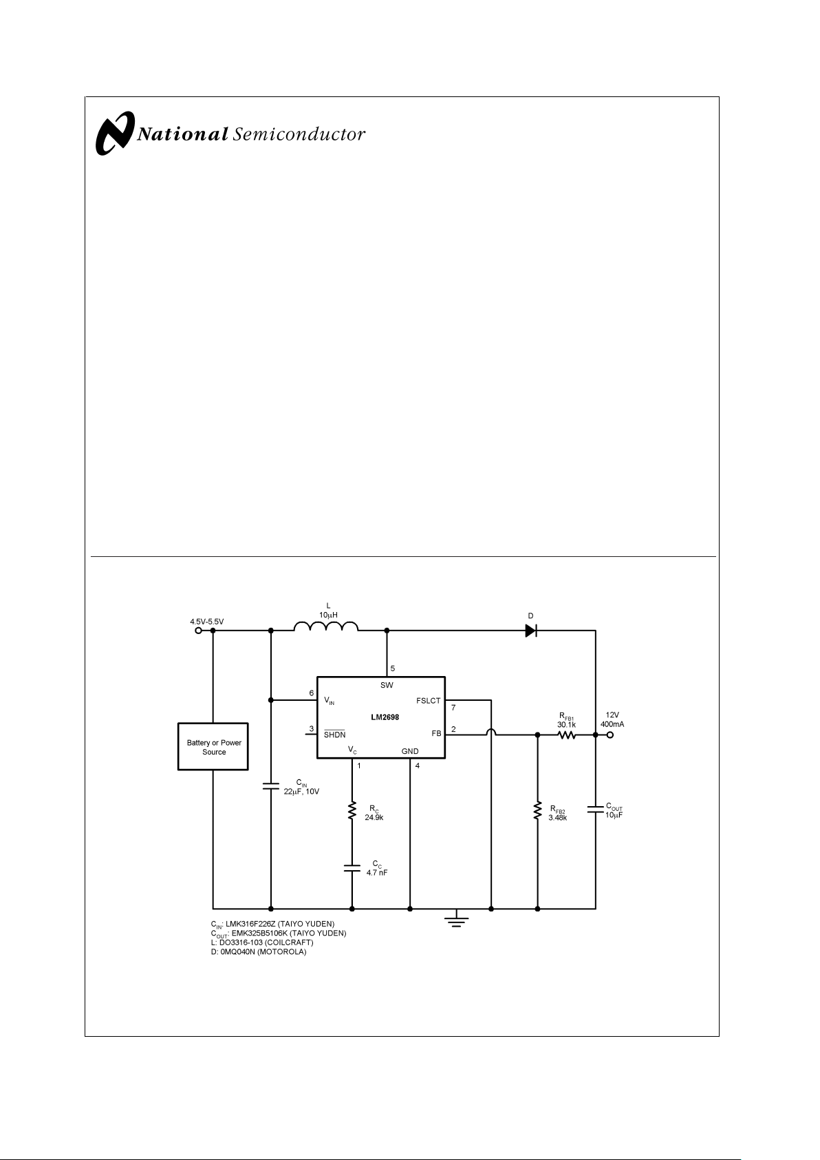
capable of supplying 12V at 400mA from a 5V input. The
LM2698 can also be used in flyback or SEPIC topologies.
The LM2698 SIMPLE SWITCHER
®
features a pin selectable
switching frequency of either 600kHz or 1.25MHz. This promotes flexibility in component selection and filtering techniques. A shutdown pin is available to suspend the device
and decrease the quiescent current to 5µA. An external
compensation pin gives the user flexibility in setting frequency compensation, which makes possible the use of
small, low ESR ceramic capacitors at the output. Switchers
Made Simple
®
software is available to insure a quick, easy
and guaranteed design. The LM2698 is available in a low
profile 8-lead MSOP package.
Features
n 1.9A, 0.2Ω, internal switch (typical)
n Operating voltage as low as 2.2V
n 600kHz/1.25MHz adjustable frequency operation
n Switchers Made Simple
®
software
n 8-Lead MSOP package
Applications
n 3.3V to 5V, 5V to 12V conversion
n Distributed Power
n Set-Top Boxes
n DSL Modems
n Diagnostic Medical Instrumentation
n Boost Converters
n Flyback Converters
n SEPIC Converters
Typical Application Circuit
20012658
SIMPLE SWITCHER®is a registered trademark of National Semiconductor Corporation.
October 2001
LM2698 SIMPLE SWITCHER
®
1.35A Boost Regulator
© 2001 National Semiconductor Corporation DS200126 www.national.com
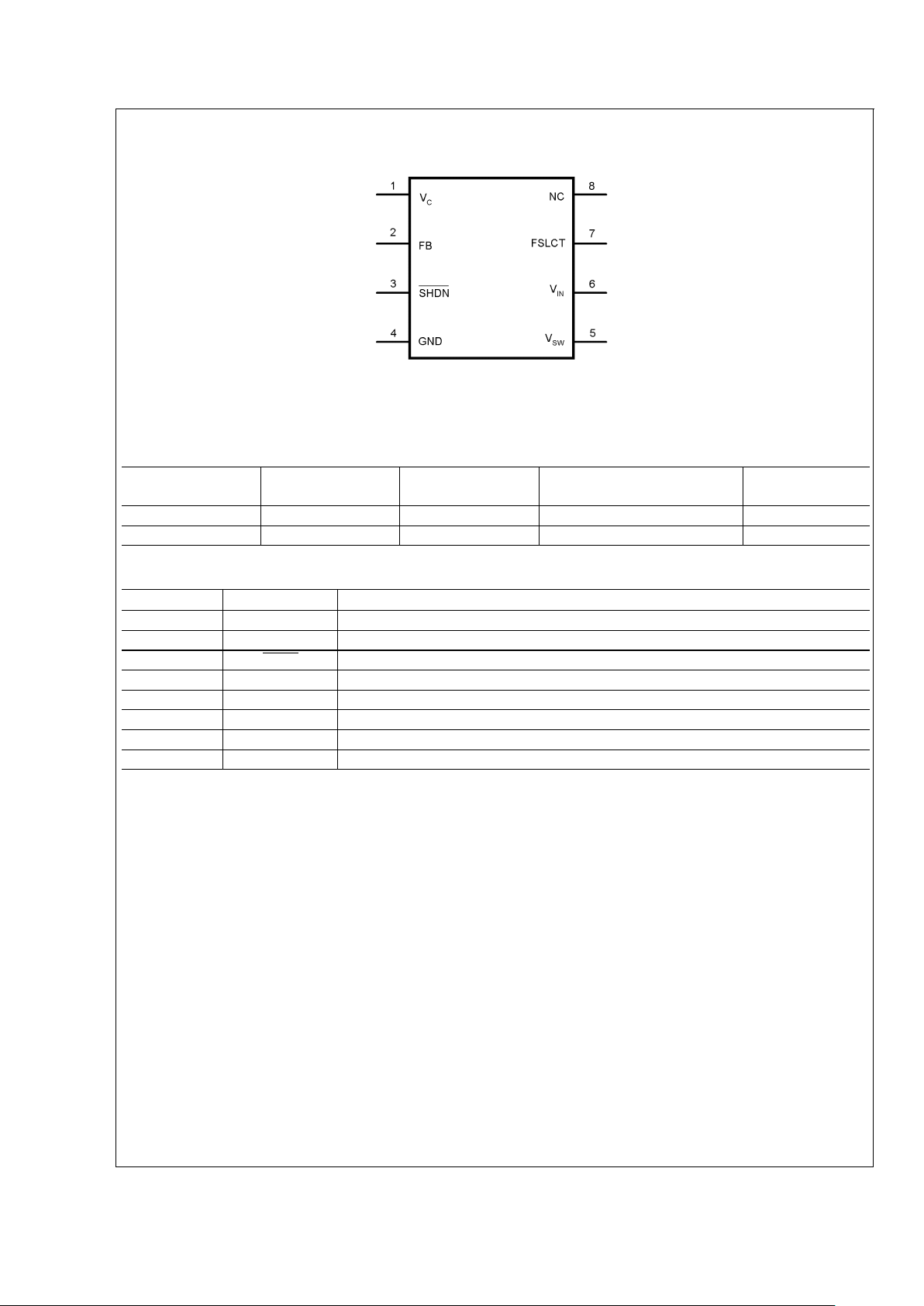
Connection Diagram
Top View
20012604
8-Lead Plastic MSOP
NS Package Number MUA08A
Ordering Information
Order Number Package Type NSC Package
Drawing
Supplied As Package ID
LM2698MM-ADJ MSOP-8 MUA08A 1000 Units, Tape and Reel S22B
LM2698MMX-ADJ MSOP-8 MUA08A 3500 Units, Tape and Reel S22B
Pin Description
Pin Name Function
1V
C
Compensation network connection. Connected to the output of the voltage error amplifier.
2 FB Output voltage feedback input.
3 SHDN
Shutdown control input, active low.
4 GND Analog and power ground.
5V
SW
Power switch input. Switch connected between SW pin and GND pin.
6V
IN
Analog power input.
7 FSLCT Switching frequency select input. V
IN
= 1.25MHz. Ground = 600kHz.
8 NC Connect to ground.
LM2698
www.national.com 2
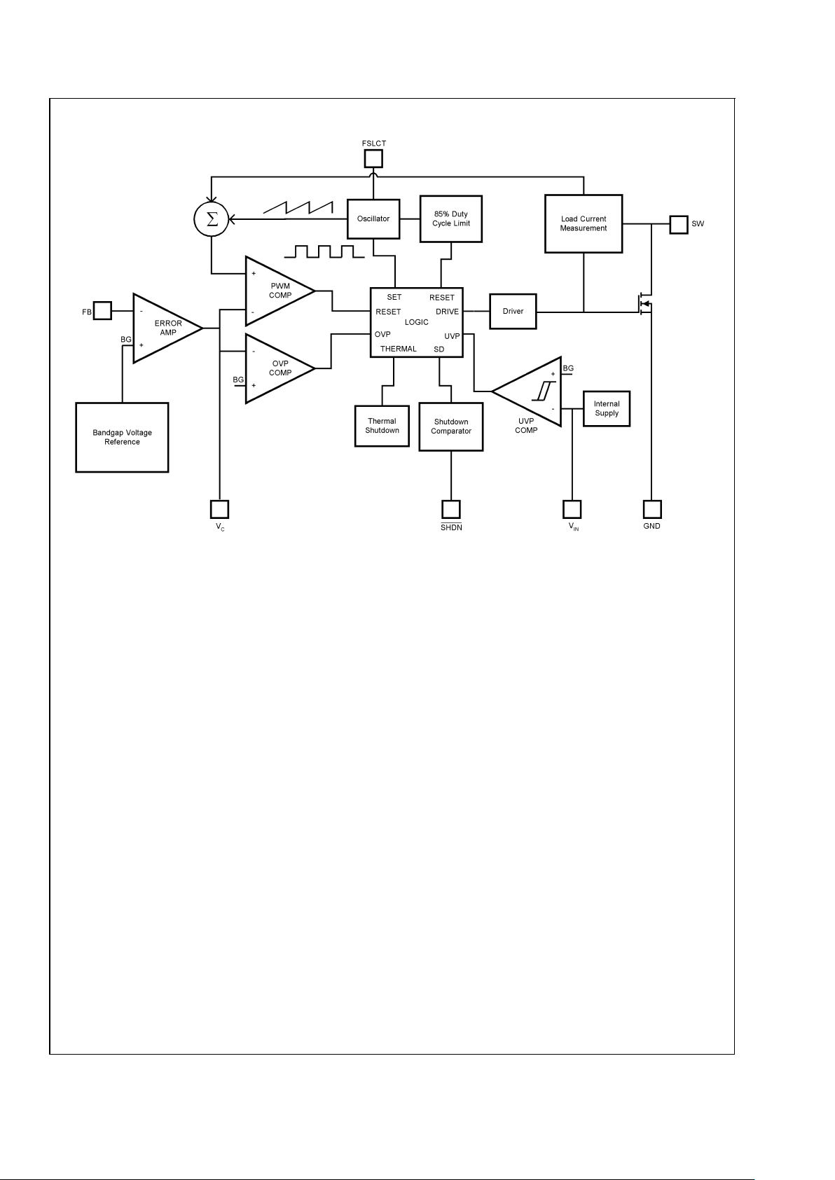
Block Diagram
20012603
LM2698
www.national.com3
Absolute Maximum Ratings (Note 1)
If Military/Aerospace specified devices are required,
please contact the National Semiconductor Sales Office/
Distributors for availability and specifications.
V
IN
−0.3V ≤ VIN≤ 12V
SW Voltage −0.3V ≤ V
SW
≤ 18V
FB Voltage −0.3V ≤ V
FB
≤ 7V
V
C
Voltage 0.965<V
C
<
1.565
SHDN Voltage
(Note 2) −0.3V ≤ V
SHDN
≤ 7V
FSLCT
(Note 2) −0.3V ≤ V
FSLCT
≤ 12V
Maximum Junction
Temperature
150˚C
Power Dissipation (Note 3) Internally Limited
Lead Temperature 300˚C
Vapor Phase (60 sec.) 215˚C
Infrared (15 sec.) 220˚C
ESD Susceptibility
(Note 4)
Human Body Model
(Note 5) 2kV
Machine Model 200V
Operating Conditions
Operating Junction
Temperature Range
(Note 6) −40˚C to +125˚C
Storage Temperature −65˚C to +150˚C
Supply Voltage 2.2V to 12V
SW Voltage 0 ≤ V
SW
≤ 17.5V
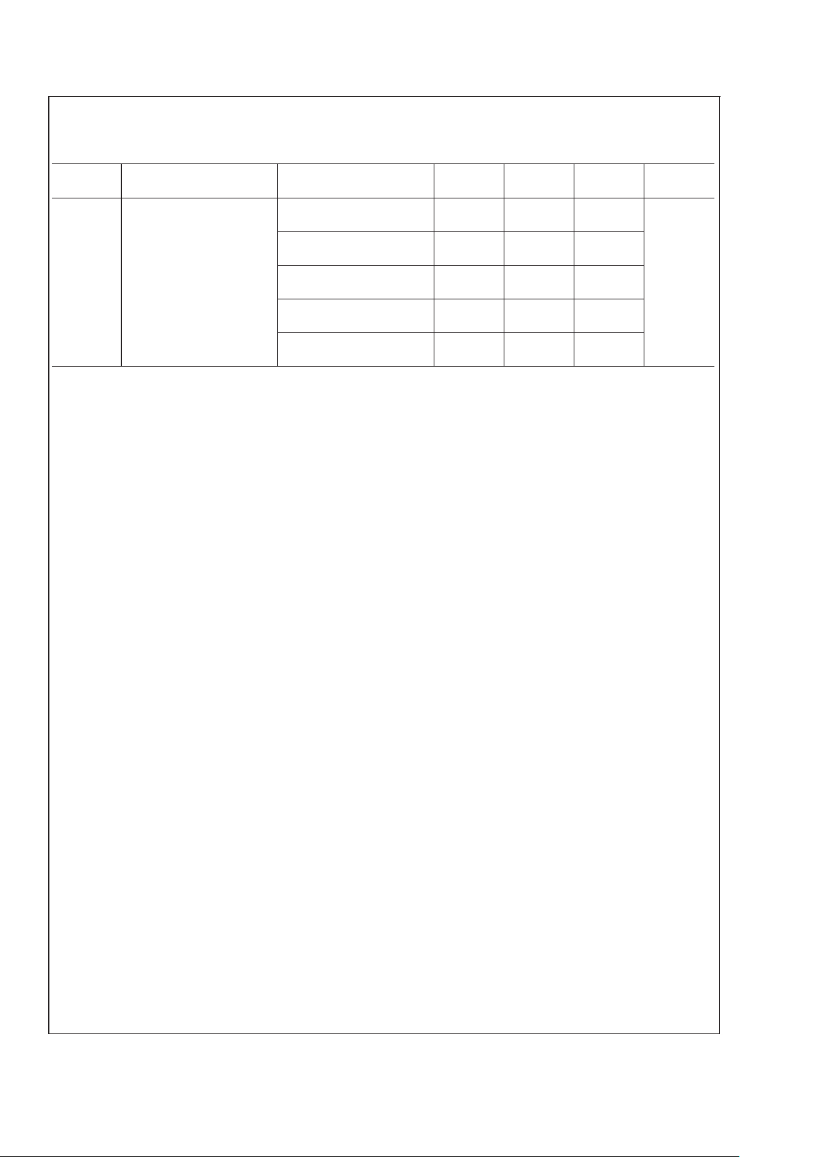
Electrical Characteristics
Specifications in standard type face are for TJ= 25˚C and those with boldface type apply over the full Operating Temperature Range (T
J
= −40˚C to +125˚C)Unless otherwise specified. VIN=2.2V and IL= 0A, unless otherwise specified.
Symbol Parameter Conditions
Min
(Note 6)
Typ
(Note 7)
Max
(Note 6)
Units
I
Q
Quiescent Current FB = 0V (Not Switching) 1.3 2.0 mA
V
SHDN
=0V 5 10 µA
V
FB
Feedback Voltage 1.2285 1.26 1.2915 V
I
CL
Switch Current Limit VIN= 2.7V (Note 8) 1.35 1.9 2.4 A
%V
FB
/∆VINFeedback Voltage Line
Regulation
2.2V ≤ VIN≤ 12.0V 0.013 0.1 %/V
I
B
FB Pin Bias Current
(Note 9)
0.5 20 nA
V
IN
Input Voltage Range 2.2 12 V
g
m
Error Amp Transconductance ∆I = 5µA 40 135 290 µmho
A
V
Error Amp Voltage Gain 120 V/V
D
MAX
Maximum Duty Cycle FSLCT = Ground 78 85 %
D
MIN
Minimum Duty Cycle FSLCT = Ground 15 %
FSLCT = V
IN
30
f
S
Switching Frequency FSLCT = Ground 480 600 720 kHz
FSLCT = V
IN
1 1.25 1.5 MHz
I
SHDN
Shutdown Pin Current V
SHDN
=V
IN
0.01 0.1 µA
V
SHDN
=0V −0.5 -1
I
L
Switch Leakage Current VSW= 18V 0.01 3 µA
R
DS(ON)
Switch R
DS(ON)
VIN= 2.7V, ISW= 1A 0.2 0.4 Ω
TH
SHDN
SHDN Threshold Voltage Output High 0.6 0.9 V
Output Low 0.3 0.6 V
UVP On Threshold 1.95 2.05 2.2 V
Off Threshold 1.85 1.95 2.1 V
LM2698
www.national.com 4
Electrical Characteristics (Continued)
Specifications in standard type face are for TJ= 25˚C and those with boldface type apply over the full Operating Temperature Range (T
J
= −40˚C to +125˚C)Unless otherwise specified. VIN=2.2V and IL= 0A, unless otherwise specified.
Symbol Parameter Conditions
Min
(Note 6)
Typ
(Note 7)
Max
(Note 6)
Units
θ
JA
Thermal Resistance Junction to Ambient
(Note 10)
235 ˚C/W
Junction to Ambient
(Note 11)
225
Junction to Ambient
(Note 12)
220
Junction to Ambient
(Note 13)
200
Junction to Ambient
(Note 14)
195
Note 1: Absolute maximum ratings are limits beyond which damage to the device may occur. Operating Ratings are conditions for which the device is intended to
be functional, but device parameter specifications may not be guaranteed. For guaranteed specifications and test conditions, see the Electrical Characteristics.
Note 2: Shutdown and voltage frequency select should not exceed V
IN
.
Note 3: The maximum allowable power dissipation is a function of the maximum junction temperature, T
J
(MAX), the junction-to-ambient thermal resistance, θJA,
and the ambient temperature, T
A
. See the Electrical Characteristics table for the thermal resistance of various layouts. The maximum allowable power dissipation
at any ambient temperature is calculated using: P
D
(MAX) = (T
J(MAX)−TA
)/θJA. Exceeding the maximum allowable power dissipation will cause excessive die
temperature, and the regulator will go into thermal shutdown.
Note 4: The human body model is a 100 pF capacitor discharged through a 1.5kΩ resistor into each pin. The machine model is a 200pF capacitor discharged
directly into each pin.
Note 5: ESD susceptibility using the human body model is 500V for V
C
.
Note 6: All limits guaranteed at room temperature (standard typeface) and at temperature extremes (bold typeface). All room temperature limits are 100% tested
or guaranteed through statistical analysis.All limits at temperature extremes are guaranteed via correlation using standard Statistical Quality Control (SQC) methods.
All limits are used to calculate Average Outgoing Quality Level (AOQL).
Note 7: Typical numbers are at 25˚C and represent the most likely norm.
Note 8: This is the switch current limit at 0% duty cycle. The switch current limit will change as a function of duty cycle. See Typical performance Characteristics
section for I
CL
vs. V
IN
Note 9: Bias current flows into FB pin.
Note 10: Junction to ambient thermal resistance (no external heat sink) for the MSO8 package with minimal trace widths (0.010 inches) from the pins to the circuit.
See ’Scenario ’A’’ in the Power Dissipation section.
Note 11: Junction to ambient thermal resistance for the MSO8 package with minimal trace widths (0.010 inches) from the pins to the circuit and approximately
0.0191 sq. in. of copper heat sinking. See ’Scenario ’B’’ in the Power Dissipation section.
Note 12: Junction to ambient thermal resistance for the MSO8 package with minimal trace widths (0.010 inches) from the pins to the circuit and approximately
0.0465 sq. in. of copper heat sinking. See ’Scenario ’C’’ in the Power Dissipation section.
Note 13: Junction to ambient thermal resistance for the MSO8 package with minimal trace widths (0.010 inches) from the pins to the circuit and approximately
0.2523 sq. in. of copper heat sinking. See ’Scenario ’D’’ in the Power Dissipation section.
Note 14: Junction to ambient thermal resistance for the MSO8 package with minimal trace widths (0.010 inches) from the pins to the circuit and approximately
0.0098 sq. in. of copper heat sinking on the top layer and 0.0760 sq. in. of copper heat sinking on the bottom layer, with three 0.020 in. vias connecting the planes.
See ’Scenario ’E’’ in the Power Dissipation section.
LM2698
www.national.com5
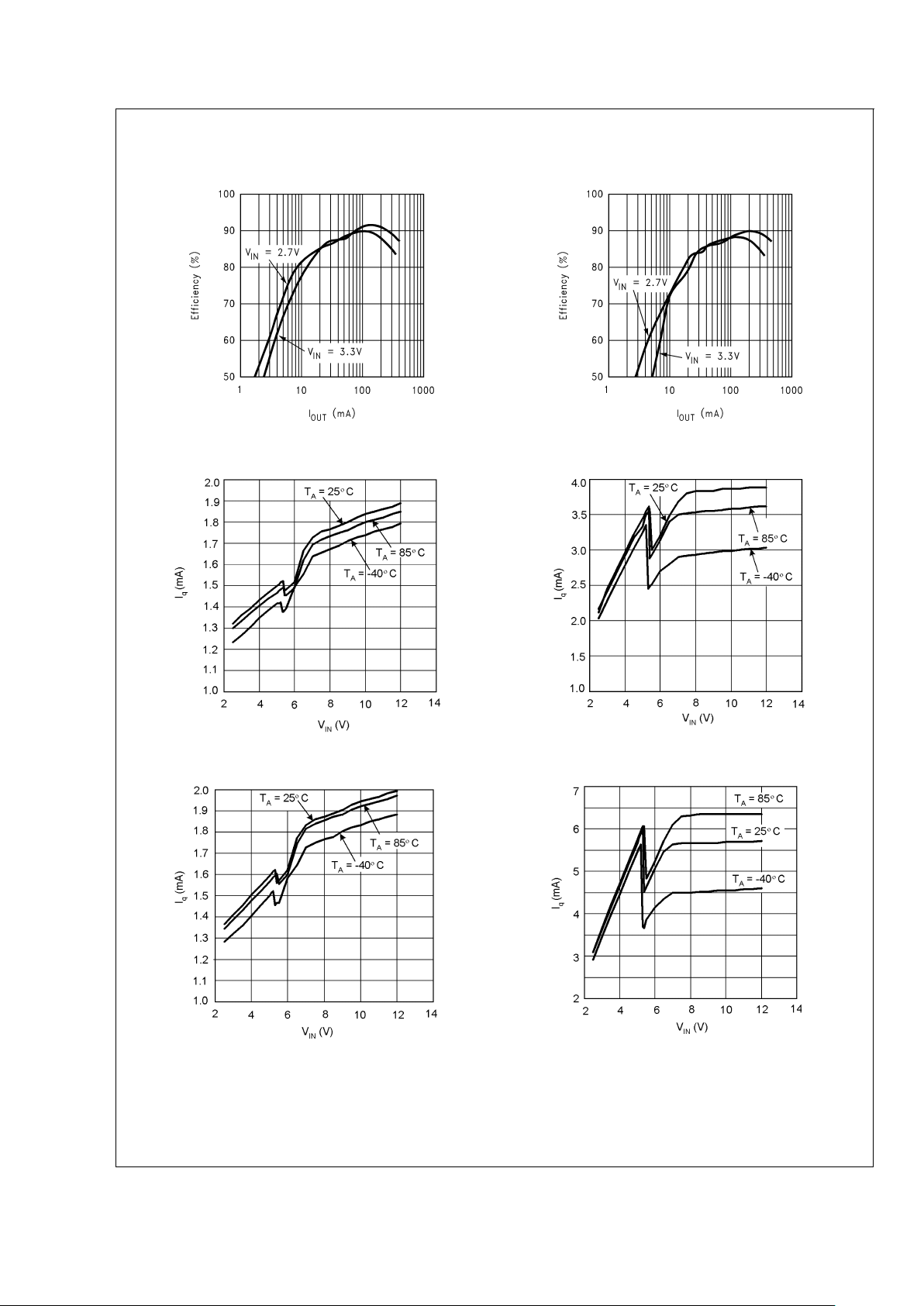
Typical Performance Characteristics
Efficiency vs Load Current
(V
OUT
= 8V, fS= 600kHz)
Efficiency vs Load Current
(V
OUT
= 8V, fS= 1.25MHz)
20012667 20012666
Iqvs VIN(600 kHz, non-switching) Iqvs VIN(600 kHz, switching)
20012618
20012619
Iqvs. VIN(1.25MHz, non-switching) Iqvs VIN(1.25MHz, switching)
20012622
20012617
LM2698
www.national.com 6
 Loading...