

NSC LM2686MTCX, LM2686MTC Datasheet
LM2686
Regulated Switched Capacitor Voltage Converter
LM2686 Regulated Switched Capacitor Voltage Converter
November 1999
General Description
The LM2686 CMOS charge-pump voltage converter operates as an input voltage doubler and a +5V regulator for an
input voltage in the range of +2.85V to +6.5V. Three low cost
capacitors are used in this circuit to provide up to 50mA of
output current at +5.0V (
130 kHz switching frequency to reduce output resistance
and voltage ripple. With an operating current of only 450µA
(operating efficiency greater than 80%with most loads) and
6.0µA typical shutdown current, the LM2686 is ideal for use
in battery powered systems. The device is in a small 14-pin
TSSOP package.
±
5%). The LM2686 operates at a
Features
n +5V regulated output
n Doubles input supply voltage
n TSSOP 14 package
n 80%typical conversion efficiency at 25mA
n Input voltage range of 2.85V to 6.5V
n Independent shutdown control pins
Applications
n Cellular phones
n Pagers
n PDAs
n Handheld Instrumentation
n 3.3V to 5V Voltage Conversion Applications
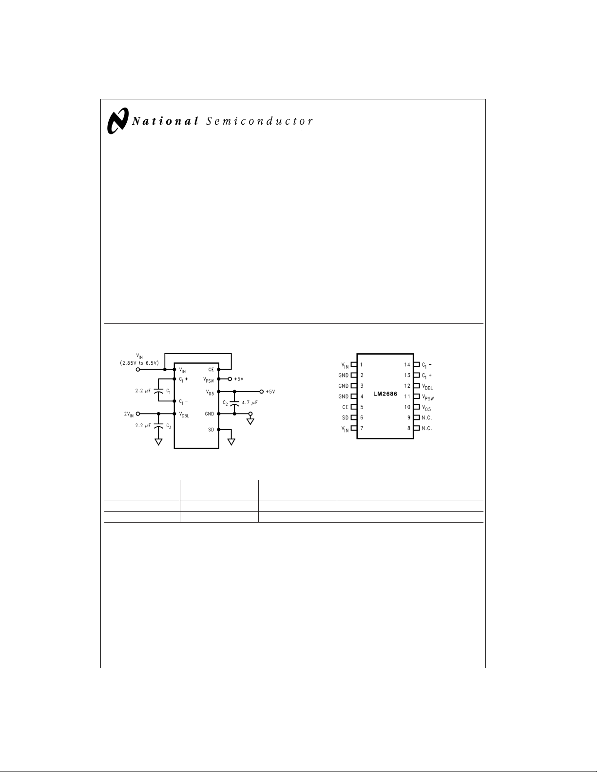
Typical Application and Connection Diagram
DS101141-1
Ordering Information
DS101141-2
14-Pin TSSOP
Order Number Package Type
LM2686MTC TSSOP-14 MTC14 94 Units, Rail
LM2686MTCX TSSOP-14 MTC14 2.5k Units, Tape and Reel
© 1999 National Semiconductor Corporation DS101141 www.national.com
NSC Package
Drawing
Supplied As
Pin Description
LM2686
Pin No. Name Function
1V
2 GND
3 GND
4 GND
5 CE Chip enable input. This pin is high for normal operation and low for shutdown and V
6
7V
8 NC No connection.
9 NC No connection.
10 V
11 V
12 V
13 C
14 C
*
All VINpins, pin 1 and pin 7 must be tied together for proper operation.
**
All ground pins, pin 2, pin 3 and pin 4 must be tied together for proper operation.
SD
PSW
DBL
*
IN
**
**
**
Power supply input voltage.
Power supply ground.
Power supply ground.
Power supply ground.
load disconnect.
Shutdown input. This pin is low for normal operation and high for shutdown and V
load disconnect.
*
IN
05
Power supply input voltage.
Regulated +5V output.
V05output connected through a series switch, PSW.
Output of doubled input voltage.
+
1
−
1
The positive terminal of doubling charge-pump capacitor, C1.
The negative terminal of doubling charge-pump capacitor, C1.
PSW
PSW
www.national.com 2

Absolute Maximum Ratings (Note 1)
If Military/Aerospace specified devices are required,
please contact the National Semiconductor Sales Office/
Distributors for availability and specifications.
Supply Voltage (V
SD, CE (GND − 0.3V) to
V
Continuous Output Current 80mA
05
V
Short-Circuit Duration to GND
05
(Note 2)
Continuous Power Dissipation (T
=
25˚C) (Note 3)
to GND) 6.8V
IN
(V
In
Indefinite
A
600mW
+ 0.3V)
T
(Note 3) 150˚C
JMAX
θ
(Note 3) 140˚C/W
JA
Operating Ambient Temp. Range −40˚C to 85˚C
Operating Junction Temperature
Range −40˚C to 125˚C
Storage Temp. Range −65˚C to 150˚C
Lead Temp. (Soldering, 10 sec.) 300˚C
ESD Rating (Note 4) 2kV
Electrical Characteristics
Limits with standard typeface apply for T
otherwise specified V
IN
=
3.6V, C
Symbol Parameter Conditions Min Typ Max Units
+
Supply Voltage 2.85 6.5 V
V
I
Supply Current No Load 450 950 µA
Q
I
V
I
(+5V) Output Current at V
L
F
P
V
G
G
LOAD
R
Note 1: Absolute Maximum Ratings indicate limits beyond which damage to the device may occur. Operating Ratings indicate conditions for which the device is intended to be functional, but do not guarantee specific performance limits. For guaranteed specifications and test conditions, see the Electrical Characteristics.
Note 2: V
Note 3: The maximum allowable power dissipation is calculated by usingP
ambient temperature and θ
Note 4: The human body model is a 100pF capacitor discharged through a 1.5kΩ resistor into each pin.
Note 5: In the typical operating circuit, capacitors C
reduce output voltage and efficiency.
Note 6: The 50mA maximum current assumes no current is drawn from V
Shutdown Supply Current V
SD
Shutdown Pin Input Voltage for
SD
CE, SD
Switch Frequency 85 130 180 kHz
SW
Average Power Efficiency at V052.85V<V
EFF
Output Regulation 1mA<I
05
Line Regulation 2.85V<V
LINE
05
Load Regulation 1mA<I
Series Switch Resistance from
SW
to V
V
05
PSW
may be shorted to GND without damage. For temperature above 85˚C, V05must not be shorted to GND or device may be damaged.
05
is the junction-to-ambient thermal resistance of the specified package.
JA
=
25˚C, and limits in boldface type apply over the full temperature range. Unless
J
=
=
C
2.2µF. C
1
3
=
4.7µF. (Note 5)
2
=
6.5V 6 30 µA
IN
Logic Input High@6.5V 2.4
@
Logic Input Low
2.85V<V
=
25mA to GND 82
I
L
L
(Note 6)
<
I
1mA
L
(Note 6)
<
V
3.6V
IN
L
>
V
2.85V 5.0 Ω
IN
and C3are 2.2µF, 0.3Ω maximum ESR capacitors. Capacitors with higherESRwillincrease output resistance,
1
6.5V 0.8
<
6.5V 50 mA
IN
<
6.5V
IN
<
50mA, V
<
50mA, V
<
IN
<
<
50mA, V
DMAX
pin. See Voltage Doubler section in the Detailed Device Description.
DBL
=
6.5V
IN
=
6.5V
IN
4.848 5.05 5.252 V
4.797 5.05 5.303 V
3.6V 0.25
6.5V 0.05
=
6.5V 0.3 1.0
IN
=
(T
JMAX—TA
)/θJA, where T
is the maximum junction temperature,TAis the
JMAX
V
%
%
%
LM2686
/V
www.national.com3
 Loading...