

NSC LM2682MM, LM2682M, LM2682MMX Datasheet

LM2682
Switched Capacitor Voltage Doubling Inverter
LM2682 Switched Capacitor Voltage Doubling Inverter
November 1999
General Description
The LM2682 is a CMOS charge-pump voltage inverter capable of converting positive voltage in the range of +2.0V to
+5.5V to the corresponding doubled negative voltage of
−4.0V to −11.0V respectively. The LM2682 uses three low
cost capacitors to provide 10 mA of output current without
the cost, size, and EMI related to inductor based circuits.
With an operating current of only 150µAandanoperatingefficiency greater than 90%with most loads, the LM2682 provides ideal performance for battery powered systems. The
LM2682 offers a switching frequency of 6 kHz.
Features
n Inverts then doubles input supply voltage
n Small MSOP-8 package (mini SO-8) and SO-8 package
n 90Ω typical output impedance
n 94%typical power efficiency at 10 mA
Applications
n LCD contrast biasing
n GaAs power amplifier biasing
n Interface power supplies
n Handheld instrumentation
n Laptop computers and PDAs
Typical Operating Circuit and Pin Configuration
8-Pin MSOP
or 8-Pin SOIC
DS100997-2
DS100997-1
Ordering Information
Order Number Package Package Number Package Marking Supplied As
LM2682MM MSOP-8 MUA08A S11A Tape and Reel (1000 units/reel)
LM2682MMX MSOP-8 MUA08A S11A Tape and Reel (3500 units/reel)
LM2682M SO-8 M08A LM2682M Rail (95 units/rail)
LM2682MX SO-8 M08A LM2682M Tape and Reel (2500 units/reel)
© 1999 National Semiconductor Corporation DS100997 www.national.com

Absolute Maximum Ratings (Note 1)
If Military/Aerospace specified devices are required,
LM2682
please contact the National SemiconductorSales Office/
Distributors for availability and specifications.
Input Voltage (V
V
dV/dT 1V/µsec
IN
V
OUT
V
Short-Circuit Duration Continuous
OUT
Storage Temperature −65˚C to +150˚C
Lead Temperature Soldering +300˚C
) +5.8V
IN
−11.6V
MSOP-8 300 mW
SO-8 470 mW
T
JMAX
Operating Ratings
ESD Susceptibility (Note 3)
Human Body Model
Machine Model
Ambient Temp. Range −40˚C to +85˚C
Junction Temp. Range −40˚C to +125˚C
Power Dissipation (Note 2)
LM2682
Electrical Characteristics
typeface apply over the full operating ambient temperature range, −40˚C to +85˚C, limits with standard typeface apply for T
=
25˚C.
V
IN
=
5V and C
=
=
=
C
C
1
3.3µF unless otherwise specified. Limits with bold
2
3
+150˚C
2kV
200V
A
Symbol Parameter Conditions Min Typical
Max Units
(Note 4)
V
IN
I
IN
R
OUT
Supply Voltage Range R
Supply Current Open Circuit, No Load 150 300
V
Source Resistance I
OUT
=
2kΩ 2.0 5.5 V
L
400
=
10 mA 90 150 Ω
L
µA
200
=
I
5 mA, V
f
OSC
f
SW
η
POWER
η
VOLTAGE
Note 1: Absolute Maximum Ratings are thosevalues beyond which damage to the device may occur. Operating Ratings indicate conditions for whichthe device is
intended to be functional, but do not guarantee specific performance limits. For guaranteed specifications and test conditions, see the Electrical Characteristics.
Note 2: The maximum power dissipationmustbede-rated at elevated temperatures (only needed for T
ture), θ
maximum power dissipation at any temperature is:
PDiss
Note 3: The human body model is a 100 pF capacitor discharged through a 1.5 kΩ resistor into each pin.The machine model is a 200pF capacitor discharged di-
rectly into each pin.
Note 4: Typical numbers are at 25˚C and represent the most likely norm.
Note 5: The output switches operate at one half of the oscillator frequency, f
Note 6: The minimum specification is guaranteed by design and is not tested.
Oscillator Frequency (Note 5) 12 30 kHz
Switching Frequency (Note 5) 6 15 kHz
Power Efficiency R
Voltage Conversion Efficiency 99.9
(junction to ambient thermal resistance) and TA(ambient temperature). θ
J-A
MAX
=
(T
JMAX−TA
)/θ
up to the value listed in the Absolute Maximum Ratings.
J-A
L
=
L
=
2 V 110 250 Ω
IN
2k (Note 6) 90 93
>
85˚C) and is limited by T
is 140˚C/W for the SO-8 package and 220˚C/W for the MSOP-8 package. The
J-A
=
.
2f
OSC
SW
A
JMAX
%
%
(maximum junction tempera-
Pin Description
Pin Number Symbol Description
1C
2C
3C
4V
5 GND Device ground
6V
7C
8 NC No Connection
− Capacitor C1negative terminal
1
+ Capacitor C2positive terminal
2
− Capacitor C2negative terminal
2
Negative output voltage (−2VIN)
OUT
Power supply voltage
IN
+ Capacitor C1positive terminal
1
www.national.com 2
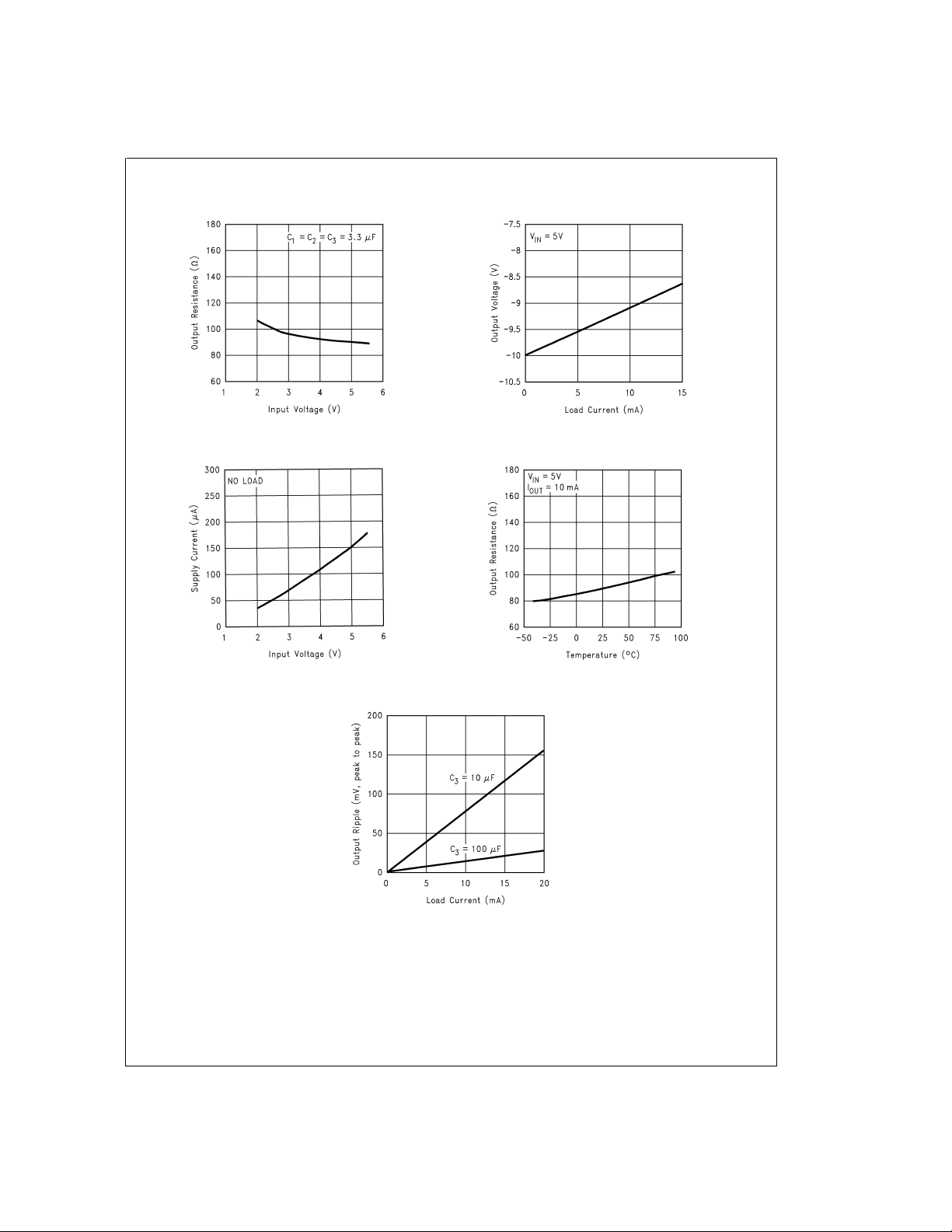
Typical Performance Charactistics V
Output Resistance vs Input Voltage
IN
=
5V and T
=
25˚C unless otherwise noted.
A
Output Voltage vs Load Current
LM2682
Supply Current vs Input Voltage
Output Voltage Ripple vs Load Current
DS100997-6
DS100997-8
DS100997-7
Output Resistance vs Temperature
DS100997-9
DS100997-10
www.national.com3
 Loading...