

NSC LM2650MX-ADJ, LM2650M-ADJ Datasheet
LM2650
Synchronous Step-Down DC/DC Converter
LM2650 Synchronous Step-Down DC/DC Converter
June 1999
General Description
The LM2650 is a step-down DC/DC converter featuring high
efficiency over a 3A to milliamperes load range. This feature
makes the LM2650 an ideal fit in battery-powered applications that demand long battery life in both run and standby
modes.
The LM2650 alsofeatures a logic-controlled shutdown mode
in which it draws at most 25µA from the input power supply.
The LM2650 employs a fixed-frequency pulse-width modulation (PWM) and synchronous rectification to achieve very
high efficiencies. In many applications, efficiencies reach
95%+ for loads around 1A and exceed 90%for moderate to
heavy loads from 0.2A to 2A.
A low-power hysteretic or ″sleep″ mode keeps efficiencies
high at light loads. The LM2650 enters and exits sleep mode
automatically as the load crosses ″sleep in″ and ″sleep out″
thresholds. The LM2650 provides nodes for programming
both thresholds via external resistors. A logic input allows the
user to override the automatic sleep feature and keep the
LM2650 in PWM mode regardless of the load level.
An optional soft-start feature limits current surges from the
input power supply at start up and provides a simple means
of sequencing multiple power supplies.
Typical Application
Features
n Ultra high efficiencies (95%possible)
n High efficiency over a 3A to milliamperes load range
n Synchronous switching of internal NMOS power FETs
n Wide input voltage range (4.5V to 18V)
n Output voltage adjustable from 1.5V to 16V
n Automatic low-power sleep mode
n Logic-controlled micropower shutdown (I
n Frequency adjustable up to 300 kHz
n Frequency synchronization with external signal
n Programmable soft-start
n Short-circuit current limiting
n Thermal shutdown
n Available in 24-lead Small-Outline package
QSD
≤ 25 µA)
Applications
n Notebook and palmtop personal computers
n Portable data terminals
n Modems
n Portable Instruments
n Global positioning devices (GPSs)
n Battery-powered digital devices
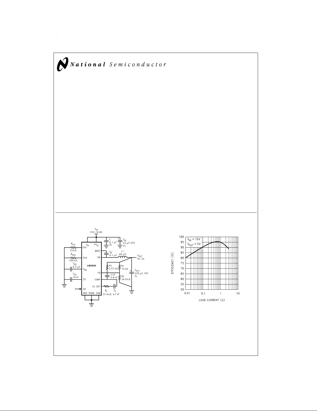
LM2650-ADJ Efficiency
DS012848-1
Converting a Four-Cell Li Ion Battery to 5V
© 1999 National Semiconductor Corporation DS012848 www.national.com
DS012848-2
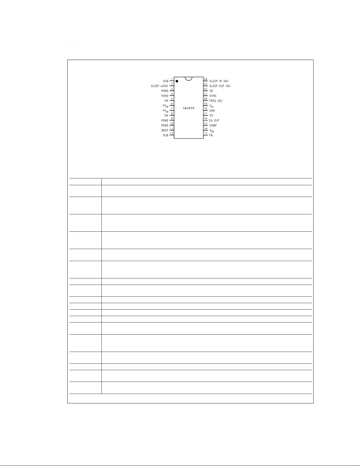
Connection Diagram
DS012848-14
24-Lead Small Outline Package (M)
Order Number LM2650M-ADJ
See Package Number M24B
Pin Descriptions
(Refer to the Block Diagrams)
Pins Description
1, 12 SUB: These pins make electrical contact with the substrate of the die. Ground them. For best thermal
performance, ground them to the same large, uninterrupted copper plane as the PGND pins.
2 SLEEP LOGIC: Use this logic input to select the conversion mode; low selects PWM, high selects sleep, and
high impedance (open) permits the LM2650 to move freely and automatically between the modes, using PWM
for moderate to heavy loads and sleep for light loads.
3, 4, 9, 10 PGND: The ground return of the power stage. The power stage consists of the two power switches Q1 and
Q2, the gate drivers DH and DL, and the linear voltage regulators VRegH and VRegL. For best electrical and
thermal performance, ground these pins to a large, uninterrupted copper plane.
5, 8 SW: The output node of the power stage. It swings from slightly below ground to slightly below the voltage to
. To minimize the effects of switching noise on nearby circuitry, keep all traces originating from SW short
PV
IN
and to the point. Route all traces carrying signals well away from the SW traces.
6, 7 PV
: The positive supply rail of the power stage. Bypass each PVINpin to PGND with a 0.1 µF capacitor. Use
IN
capacitors having low ESL and low ESR, and locate them close to the IC.
11 BOOT: The positive supply rail of the high-side gate driver DH. Connect a 0.1 µF capacitor from this node to
SW. Bootstrapping action creates a supply rail about 9V above that at PV
the gate of the NMOS power FET Q1. Overriding ensures low R
13 FB: The feedback input.
14 V
: An internal regulator steps the input voltage down to a 4V rail used by the signal-level circuitry. VDDis the
DD
output node of this regulator. Bypass V
15 COMP: The inverting input of the error amplifier EA.
16 EA OUT: The output node of the error amplifier EA.
17 SS: The soft start node. Connect a capacitor from SS to GND.
18 GND: The ground return of the signal-level circuitry.
19 V
: The positive supply rail of the internal 4V regulator. Bypass VINto GND close to the IC with a 0.1 µF
IN
capacitor.
20 FREQ ADJ: The LM2650 switches at a nominal 90 kHz. Connect a resistor between FREQ ADJ and GND to
adjust the frequency up from the nominal. Use the graph under Typical performance Characteristics to select
the resistor.
21 SYNC: The synchronization input. If the switching frequency is to be synchronized with an external clock
signal, apply the clock signal here.
22 SD: Use this logic input to control shutdown; pull low for operation, high for shutdown.
23 SLEEP OUT ADJ (SOA): The value of the resistor connected between SIA and ground programs the sleep-in
threshold. Higher values program lower thresholds.
24 SLEEP IN ADJ (SIA): The value of the resistor connected between SIA and ground programs the sleep-in
threshold. Higher values program lower thresholds.
Top View
, and DH uses this rail to override
IN
.
DS(on)
to GND close to the IC with a 0.2 µF capacitor.
DD
www.national.com 2
Absolute Maximum Ratings (Note 1)
If Military/Aerospace specified devices are required,
please contact the National Semiconductor Sales Office/
Distributors for availability and specifications.
(All voltages are referenced to the PGND and GND pins.)
DC Voltage at PV
DC Voltage at SD, SLEEP LOGIC
and SYNC 15V
DC current into SW
Junction Temperature Limited by the IC
DC Power Dissipation (Note 2) 1.28W
Storage Temperature −65˚C to +150˚C
IN
and V
±
20V
7.5A
IN
Soldering Time, Temperature (Note
3)
Wave (4 seconds)
Infrared (10 seconds)
Vapor Phase (75 seconds)
260˚C
240˚C
219˚C
ESD Susceptibility (Note 4) 1.3 kV
Operating Ratings (Note 1)
Supply Voltage Range (PV
) 4.5V to 18V
V
IN
Junction Temperature Range −40˚C to +125˚C
and
IN
Electrical Characteristics
V
= 15V, V
PVIN
type apply for T
Operating Ratings.
SLEEP LOGIC
A=TJ
=
0V and V
= +25˚C. Limits appearing in boldface type apply over the full junction temperature range shown under
Symbol Parameter Conditions Typ (Note 5) Limit (Note 6) Units
V
OUT
Output Voltage R1=75 kΩ,1%,
η1 System Efficiency I
η2 System Efficiency I
V
I
I
I
R
REF
Q
QS
QSD
DS(on)
Reference Voltage V
Quiescent Current in PWM
mode
Quiescent Current in Sleep
mode
Quiescent Current in Shutdown
mode
HS DC On-Resistance
Drain-to-Source of the
High-Side Power Switch
LS DC On-Resistance
R
DS(on)
Drain-to-Source of the
Low-Side Power Switch
I
LHS
I
LLS
I
LIMIT
F
F
D
OSC
MAX
MAX
Leakage current of the
High-Side Power Switch
Leakage current of the
Low-Side Power Switch
Active Current Limit of the
High-Side Power Switch
Oscillator Frequency V
Maximum Oscillator Frequency I
Maximum Duty Cycle V
=
0V unless superseded under Conditions. Typicals and limits appearing in plain
SD
5.00
R2=25 kΩ,1%,
7.5V ≤ V
0.12A ≤ I
LOAD
F
OSC
LOAD
F
OSC
SLEEPLOGIC
V
FB
−20mV (Note 8)
IV
FB
V
SLEEPLOGIC
≤ 18V
PVIN
LOAD
=
1A, T
Not Adjusted
=
3A, T
Not Adjusted
=
=
V
REF
=
−20mV,
V
REF
=
≤ 3A
A
A
VSD=3V
(Note 8)
=
1A,
I
DS
V
SLEEPLOGIC
V
FB
V
BOOT
=
I
DS
V
FB
V
PVIN
V
SD
V
PVIN
V
SD
V
PVIN
V
BOOT
V
FB
V
SLEEPLOGIC
FB
=
=
3V,
=
24V
1A,
=
3V
=
18V, V
=
3V
=
18V, V
=
3V
=
15V,
=
24V,
=
3V,
=
=
−20 mV 90
V
REF
=
25˚C,
=
25˚C,
3V (Note 7)
3V (Note 8)
3V,
=
0V,
SW
=
18V,
SW
3V,
94
89
1.25
4.0
850
9
130
125
100
95
5.5
4.80/4.75
5.20/5.25
1.281/1.294
1.219/1.206
6.50/7.0
1.35/1.60
20/25
170/245
175/245
10
210
3.5
7.5
80/75
100/105
FREQ ADJ
=
V
FB
=
FB
F
OSC
=
100µA,(Note 9)
−20 mV
V
REF
−20 mV,
V
REF
Not Adjusted
315
270/260
360/370
97
94/93
V
V(min)
V(max)
%
%
V(min)
V(max)
mA
mA(max)
µA
mA(max)
µA
µA(max)
mΩ
mΩ(max)
mΩ
mΩ(max)
nA
µA(max)
µA
µA(max)
A
A(min)
A(max)
kHz
kHz(min)
kHz(max)
kHz
kHz(min)
kHz(max)
%
%
(min)
www.national.com3
Electrical Characteristics (Continued)
V
= 15V, V
PVIN
type apply for T
Operating Ratings.
SLEEP LOGIC
A=TJ
=
0V and V
= +25˚C. Limits appearing in boldface type apply over the full junction temperature range shown under
Symbol Parameter Conditions Typ (Note 5) Limit (Note 6) Units
D
MIN
V
DD
V
BOOT
I
SS
V
HYST
T
SD
Note 1: Absolute Maximum Ratings are limits beyond which damage to the device may occur. Operating Ratings are conditions under which the device operates
correctly. Operating ratings do not imply guaranteed performance limits. For guaranteed performance limits and associated test conditions, see the Electrical Characteristics.
Note 2: This rating is calculated using the formula P
junction temperature, and θ
78˚C/W for T
the safe dissipation of more power. See Application Notes on thermal management. The LM2650 actively limits its junction temperature to about 170˚C.
Note 3: For detailed information on soldering plastic small-outline packages, refer to the Packaging Databook published by National Semiconductor Corporation.
Note 4: ESD is applied using the human-body model, a 100pF capacitor discharged through a 1.5kΩ resistor.
Note 5: A typical is the center of characterization data taken at T
Note 6: All limits are guaranteed. The guarantee is backed with 100%testing at T
Note 7: V
Note 8: Quiescent current is the total current flowing into the P
nominal switching frequency. I
Note 9: Pulling 100µA out of FREQ ADJ simulates adjusting the oscillator frequency with a 12.5 kΩ resistor connected from FREQ ADJ to GND. The sleep mode
cannot be used at switching frequencies above 250 kHz.
Minimum Duty Cycle V
Internal Rail Voltage I
Bootstrap Regulator Voltage
(VRegH)
Soft Start Current 10
Hysteresis of the Sleep
Comparator (C2
of SD 0.95 V(max)
V
IL
V
of SD 2.10 V(min)
IH
V
of SLEEP LOGIC 0.9 V(max)
IL
V
of SLEEP LOGIC 2.0 V(min)
IH
V
of SYNC 0.50 V(max)
IL
V
of SYNC 1.45 V(min)
IH
Figure 2
TJfor Thermal Shutdown 170 ˚C
is the junction ot ambient thermal resistance of the package. The P
JA
and θJArespectively.A θJAof 78˚C represents the worst condition of no heat sinking of the M24B small-outline package. Heat sinking allows
Jmax,TA
is measured at SLEEP OUT ADJ.
REF
includes no such current.
QS
=
0V unless superseded under Conditions. Typicals and limits appearing in plain
SD
=
+50 mV,
V
FB
REF
Not Adjusted
F
OSC
=1mA 4.0
VDD
2.8
5
3.6/3.4
4.2/4.3
I
=1mA 7.5
BOOT
6.5/6.0
13.5/20.0
V
)
SLEEPLOGIC
=
3V 30
10
50
DCmax
=
)/θJA, where P
(T
Jmax−TA
= 25˚C.
A=TJ
and VINpins. IQincludes the current used to drive the gates of the two NMOS power FETsat the
VIN
A=TJ
is the absolute maximum power dissipation, T
DCmax
= 125˚C and statistical correlation for room temperature and cold limits.
rating of 1.28W results from substituting 170˚C, 70˚C and
DCmax
is the maximum
Jmax
%
V(min)
V(max)
V(min)
µA(max)
mV(min)
mV(max)
%
(min)
V
V
µA
mV
www.national.com 4
 Loading...