NSC LM1391N Datasheet

LM1391 Phase-Locked Loop
LM1391 Phase-Locked Loop
February 1995
General Description
The LM1391 integrated circuit has been designed primarily
for use in the horizontal section of TV receivers, but may
find use in other low frequency signal processing applications. It includes a stable VCO, linear pulse phase detector,
and variable duty cycle output driver.
Features
Y
Internal active regulator for improved supply rejection
Y
Uncommitted collector of output transistor
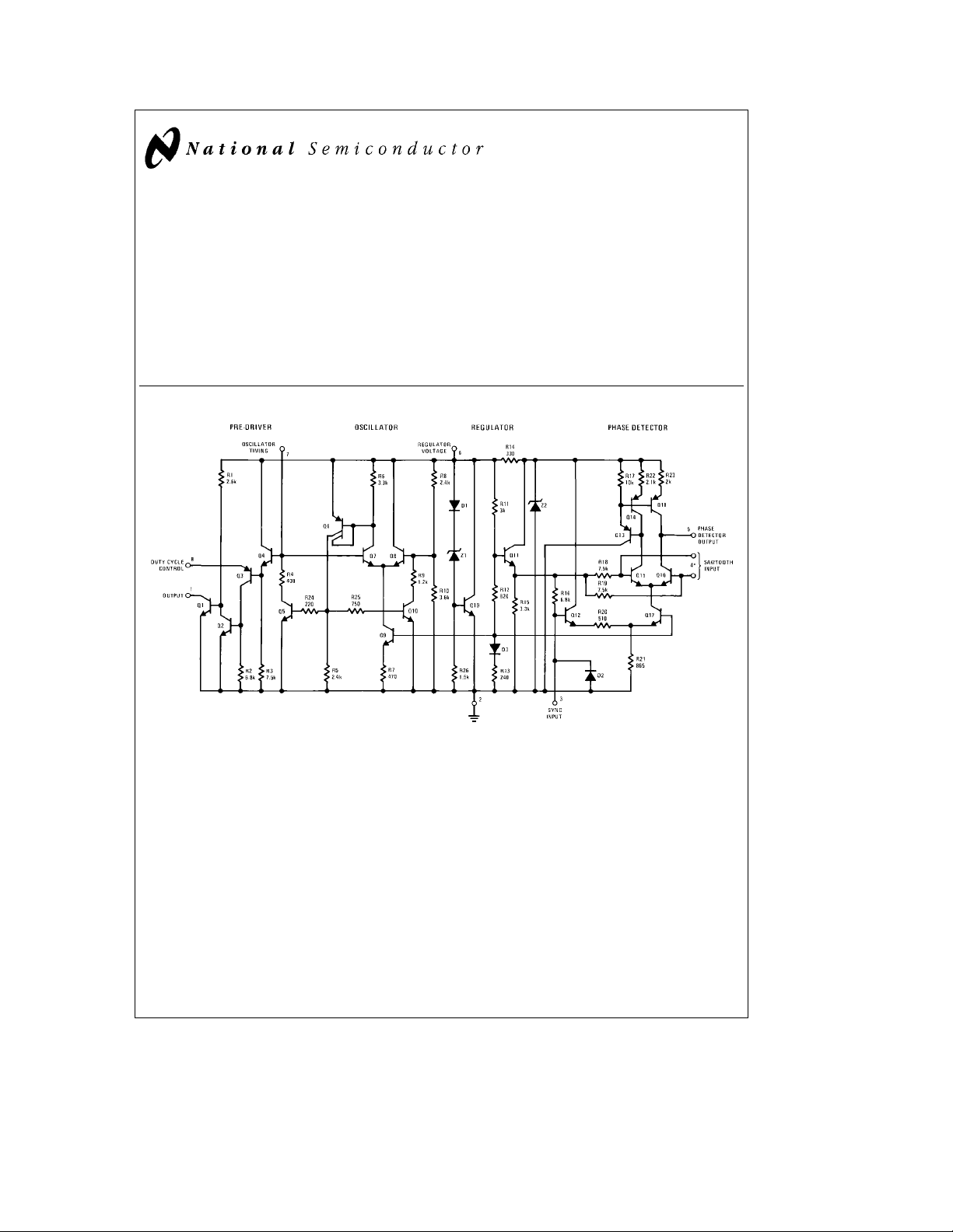
Schematic Diagram
Y
Output transistor with low saturation and high voltage
swing
Y
APC of the oscillator with a synchronizing signal
Y
DC controlled output duty cycle
Y
g
300 Hz typical pull-in
Y
Linear balanced phase detector
Y
Low thermal frequency drift
Y
Small static phase error
Y
Adjustable DC loop gain
(*) Pin 4 Base of Q16 (LM1391) for use with (a) flyback pulse
C
1995 National Semiconductor Corporation RRD-B30M115/Printed in U. S. A.
TL/H/7889
TL/H/7889– 1

Absolute Maximum Ratings
If Military/Aerospace specified devices are required,
please contact the National Semiconductor Sales
Office/Distributors for availability and specifications.
Supply Current 40 mA
Output Voltage 40 V
Output Current 30 mA
Sync Input Voltage (Pin 3) 5.0 Vp-p
DC
DC
DC
Flyback Input Voltage (Pin 4) 5.0 Vp-p
Power Dissipation (Package Limitation)
Plastic Package (Note 1) 1000 mW
Operating Temperature Range (Ambient) 0
Storage Temperature Range
Ctoa70§C
§
b
65§Ctoa150§C
Lead Temperature (Soldering, 10 sec.) 260§C
Electrical Characteristics T
e
25§C (see test circuit, all switches in position 1)
A
Parameter Conditions Min Typ Max Units
Regulated Voltage (Pin 6) I
Supply Current (Pin 6) 20 mA
Collector-Emitter Saturation Voltage I
of Output Transistor (Pin 1)
Pin 4 Voltage 2.0 V
Oscillator Pull-in Range Adjust R
Oscillator Hold-in Range Adjust R
e
22 mA
6
C1
e
DC
20 mA
H
H
8.0 8.6 9.2 V
0.30 0.40 V
g
300 Hz
g
900 Hz
DC
DC
DC
DC
Static Phase Error Dfe300 Hz 0.5 ms
Free-running Frequency Supply S1 in position 2
Dependance
Phase Detector Leakage (Pin 5) All switches in position 2
g
3.0 Hz/V
g
1.0 mA
DC
Sync Input Voltage (Pin 3) 2.0 5.0 Vp-p
Sawtooth Input Voltage (Pin 4) 1.0 3.0 Vp-p
Maximum Oscillator Frequency 500 kHz
Note 1: For operation in ambient temperatures above 25§C, the device must be derated based on a 150§C maximum junction temperature and a thermal resistance
C/W junction to ambient.
of 120
§
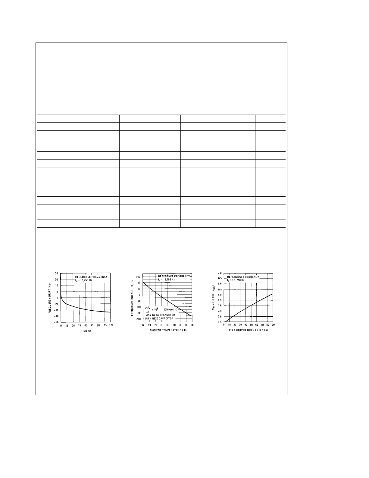
Typical Performance Characteristics
Frequency Drift vs Warm-Up
Time
Frequency vs Temperature Voltage
Output Duty Cycle vs V
M
TL/H/7889– 3
2
 Loading...