NSC LM13700N, LM13700MWC, LM13700M, LM13700MX Datasheet
LM13700/LM13700A
Dual Operational Transconductance Amplifiers with
Linearizing Diodes and Buffers
General Description
The LM13700 series consists of two current controlled
transconductance amplifiers, each with differential inputs
and a push-pull output. The two amplifiers share common
supplies but otherwise operate independently.Linearizingdiodes are providedattheinputstoreducedistortionand allow
higher input levels. The result is a 10 dB signal-to-noise improvement referenced to 0.5 percent THD. High impedance
buffers are provided which are especially designed to
complement the dynamic range of the amplifiers.The output
buffers of the LM13700 differ from those of the LM13600 in
that their input bias currents (and hence their output DC levels) are independent of I
ABC
. This may result in performance
superior to that of the LM13600 in audio applications.
Features
n gmadjustable over 6 decades
n Excellent g
m
linearity
n Excellent matching between amplifiers
n Linearizing diodes
n High impedance buffers
n High output signal-to-noise ratio
Applications
n Current-controlled amplifiers
n Current-controlled impedances
n Current-controlled filters
n Current-controlled oscillators
n Multiplexers
n Timers
n Sample-and-hold circuits
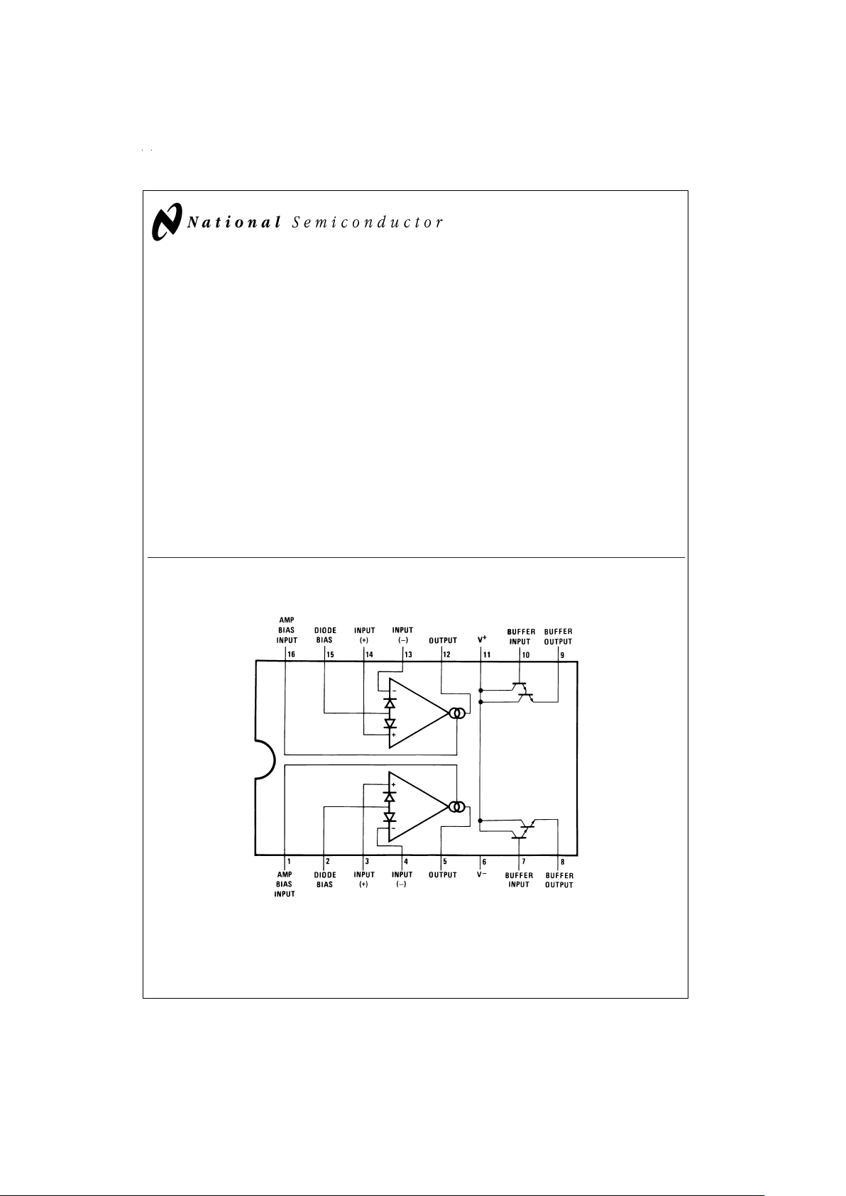
Connection Diagram
Dual-In-Line and Small Outline Packages
DS007981-2
Top View
Order Number LM13700M, LM13700N or LM13700AN
See NS Package Number M16A or N16A
May 1998
LM13700/LM13700A Dual Operational Transconductance Amplifiers with Linearizing Diodes and
Buffers
© 1999 National Semiconductor Corporation DS007981 www.national.com
Absolute Maximum Ratings (Note 1)
If Military/Aerospace specified devices are required,
please contact the National Semiconductor Sales Office/
Distributors for availability and specifications.
Supply Voltage (Note 2)
LM13700 36 V
DC
or±18V
LM13700A 44 V
DC
or±22V
Power Dissipation (Note 3) T
A
=
25˚C
LM13700N, LM13700AN 570 mW
Differential Input Voltage
±
5V
Diode Bias Current (I
D
)2mA
Amplifier Bias Current (I
ABC
)2mA
Output Short Circuit Duration Continuous
Buffer Output Current (Note 4) 20 mA
Operating Temperature Range
LM13700N, LM13700AN 0˚C to +70˚C
DC Input Voltage +V
S
to −V
S
Storage Temperature Range −65˚C to +150˚C
Soldering Information
Dual-In-Line Package
Soldering (10 sec.) 260˚C
Small Outline Package
Vapor Phase (60 sec.) 215˚C
Infrared (15 sec.) 220˚C
See AN-450 “Surface Mounting Methods and Their Effect
on Product Reliability” for other methods of soldering
surface mount devices.
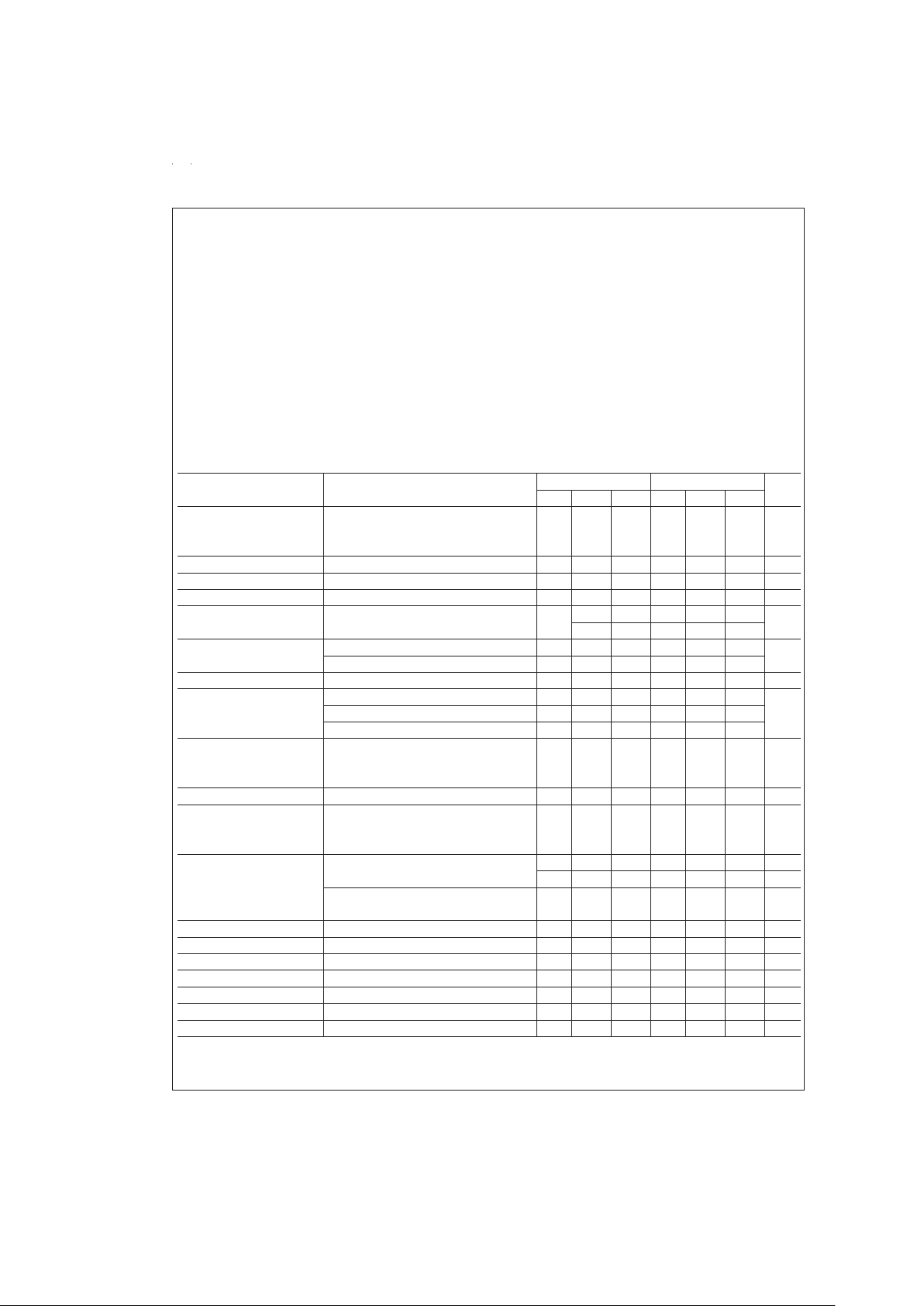
Electrical Characteristics (Note 5)
Parameter Conditions LM13700 LM13700A Units
Min Typ Max Min Typ Max
Input Offset Voltage (V
OS
) 0.4 4 0.4 1
Over Specified Temperature Range 2 mV
I
ABC
=
5 µA 0.3 4 0.3 1
V
OS
Including Diodes Diode Bias Current (ID)=500 µA 0.5 5 0.5 2 mV
Input Offset Change 5 µA ≤ I
ABC
≤ 500 µA 0.1 3 0.1 1 mV
Input Offset Current 0.1 0.6 0.1 0.6 µA
Input Bias Current Over Specified Temperature Range 0.4 5 0.4 5 µA
18 17
Forward 6700 9600 13000 7700 9600 12000 µmho
Transconductance (g
m
) Over Specified Temperature Range 5400 4000
g
m
Tracking 0.3 0.3 dB
Peak Output Current R
L
=
0, I
ABC
=
5µA 5 3 5 7
R
L
=
0, I
ABC
=
500 µA 350 500 650 350 500 650 µA
R
L
=
0, Over Specified Temp Range 300 300
Peak Output Voltage
Positive R
L
=
∞
,5µA≤I
ABC
≤ 500 µA +12 +14.2 +12 +14.2 V
Negative R
L
=
∞
,5µA≤I
ABC
≤ 500 µA −12 −14.4 −12 −14.4 V
Supply Current I
ABC
=
500 µA, Both Channels 2.6 2.6 mA
V
OS
Sensitivity
Positive ∆V
OS
/∆V
+
20 150 20 150 µV/V
Negative ∆V
OS
/∆V
−
20 150 20 150 µV/V
CMRR 80 110 80 110 dB
Common Mode Range
±12±
13.5
±12±
13.5 V
Crosstalk Referred to Input (Note 6) 100 100 dB
20 Hz
<f<
20 kHz
Differential Input Current I
ABC
=
0, Input
=
±
4V 0.02 100 0.02 10 nA
Leakage Current I
ABC
=
0 (Refer to Test Circuit) 0.2 100 0.2 5 nA
Input Resistance 10 26 10 26 kΩ
Open Loop Bandwidth 2 2 MHz
Slew Rate Unity Gain Compensated 50 50 V/µs
Buffer Input Current (Note 6) 0.5 2 0.5 2 µA
Peak Buffer Output Voltage (Note 6) 10 10 V
Note 1: “Absolute Maximum Ratings” indicate limits beyond which damage to the device may occur. Operating Ratings indicate conditions for which the device is
functional, but do not guarantee specific performance limits.
Note 2: For selections to a supply voltage above
±
22V, contact factory.
www.national.com 2
Electrical Characteristics (Note 5) (Continued)
Note 3: For operation at ambient temperatures above 25˚C, the device must be derated based on a 150˚C maximum junction temperature and a thermal resistance,
junction to ambient, as follows: LM13700N, 90˚C/W; LM13700M, 110˚C/W.
Note 4: Buffer output current should be limited so as to not exceed package dissipation.
Note 5: These specifications apply for V
S
=
±
15V,T
A
=
25˚C, amplifier bias current (I
ABC
)=500 µA, pins 2 and 15 open unless otherwise specified. The inputs to
the buffers are grounded and outputs are open.
Note 6: These specifications apply for V
S
=
±
15V, I
ABC
=
500 µA, R
OUT
=
5kΩconnected from the buffer output to −V
S
and the input of the buffer is connected
to the transconductance amplifier output.
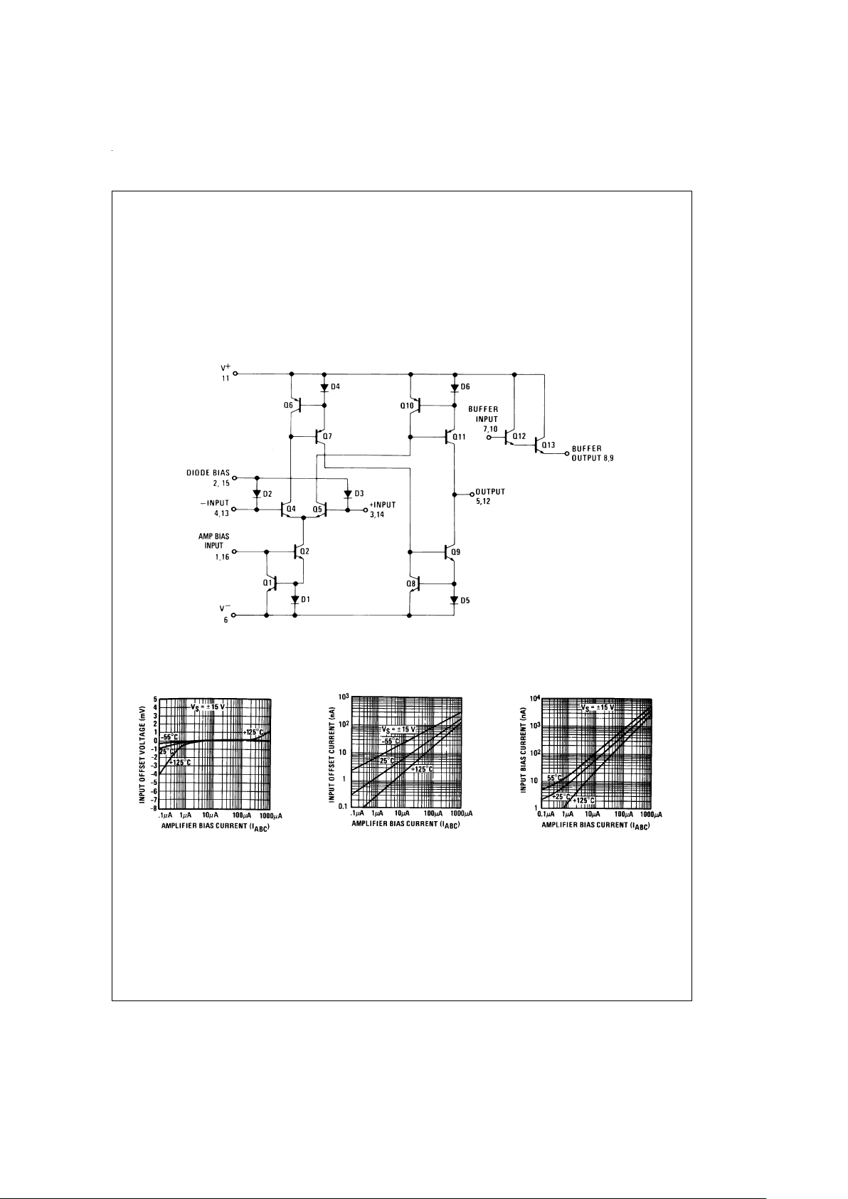
Schematic Diagram
Typical Performance Characteristics
One Operational Transconductance Amplifier
DS007981-1
Input Offset Voltage
DS007981-38
Input Offset Current
DS007981-39
Input Bias Current
DS007981-40
www.national.com3
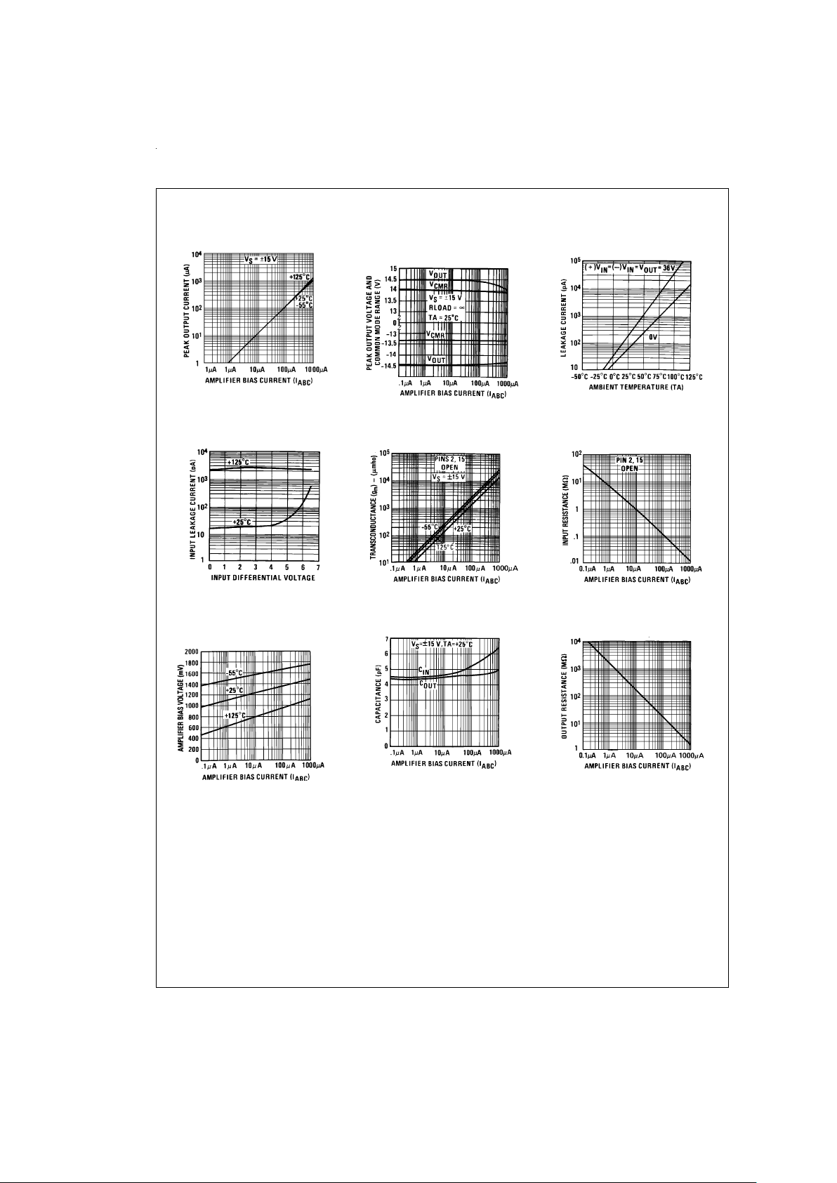
Typical Performance Characteristics (Continued)
Peak Output Current
DS007981-41
Peak Output Voltage and
Common Mode Range
DS007981-42
Leakage Current
DS007981-43
Input Leakage
DS007981-44
Transconductance
DS007981-45
Input Resistance
DS007981-46
Amplifier Bias Voltage vs
Amplifier Bias Current
DS007981-47
Input and Output Capacitance
DS007981-48
Output Resistance
DS007981-49
www.national.com 4
Typical Performance Characteristics (Continued)
Circuit Description
The differential transistor pair Q4and Q5form a transconductance stage in that the ratio of their collector currents is
defined by the differential input voltage according to the
transfer function:
(1)
where V
IN
is the differential input voltage, kT/q is approxi-
mately 26 mV at 25˚C and I
5
and I4are the collector currents
of transistors Q
5
and Q4respectively. With the exception of
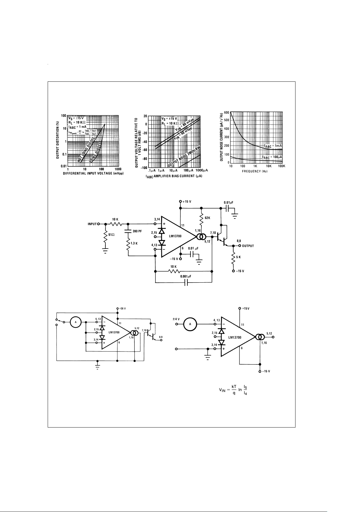
Distortion vs Differential
Input Voltage
DS007981-50
Voltage vs Amplifier
Bias Current
DS007981-51
Output Noise vs Frequency
DS007981-52
Unity Gain Follower
DS007981-5
Leakage Current Test Circuit
DS007981-6
Differential Input Current Test Circuit
DS007981-7
www.national.com5
Circuit Description (Continued)
Q
3
and Q13, all transistors and diodes are identical in size.
Transistors Q
1
and Q2with Diode D1form a current mirror
which forces the sum of currents I
4
and I5to equal I
ABC
:
I
4+I5
=
I
ABC
(2)
where I
ABC
is the amplifier bias current applied to the gain
pin.
For small differential input voltages the ratio of I
4
and I5approaches unity and the Taylor series of the In function can be
approximated as:
(3)
(4)
Collector currents I
4
and I5are not very useful by themselves
and it is necessary to subtract one current from the other.
The remaining transistors and diodes formthree current mirrors that produce an output current equalto I
5
minus I4thus:
(5)
The term in brackets is then the transconductance of the amplifier and is proportional to I
ABC
.
Linearizing Diodes
For differential voltages greater than a few millivolts,
Equa-
tion (3)
becomes less valid and the transconductance be-
comes increasingly nonlinear.
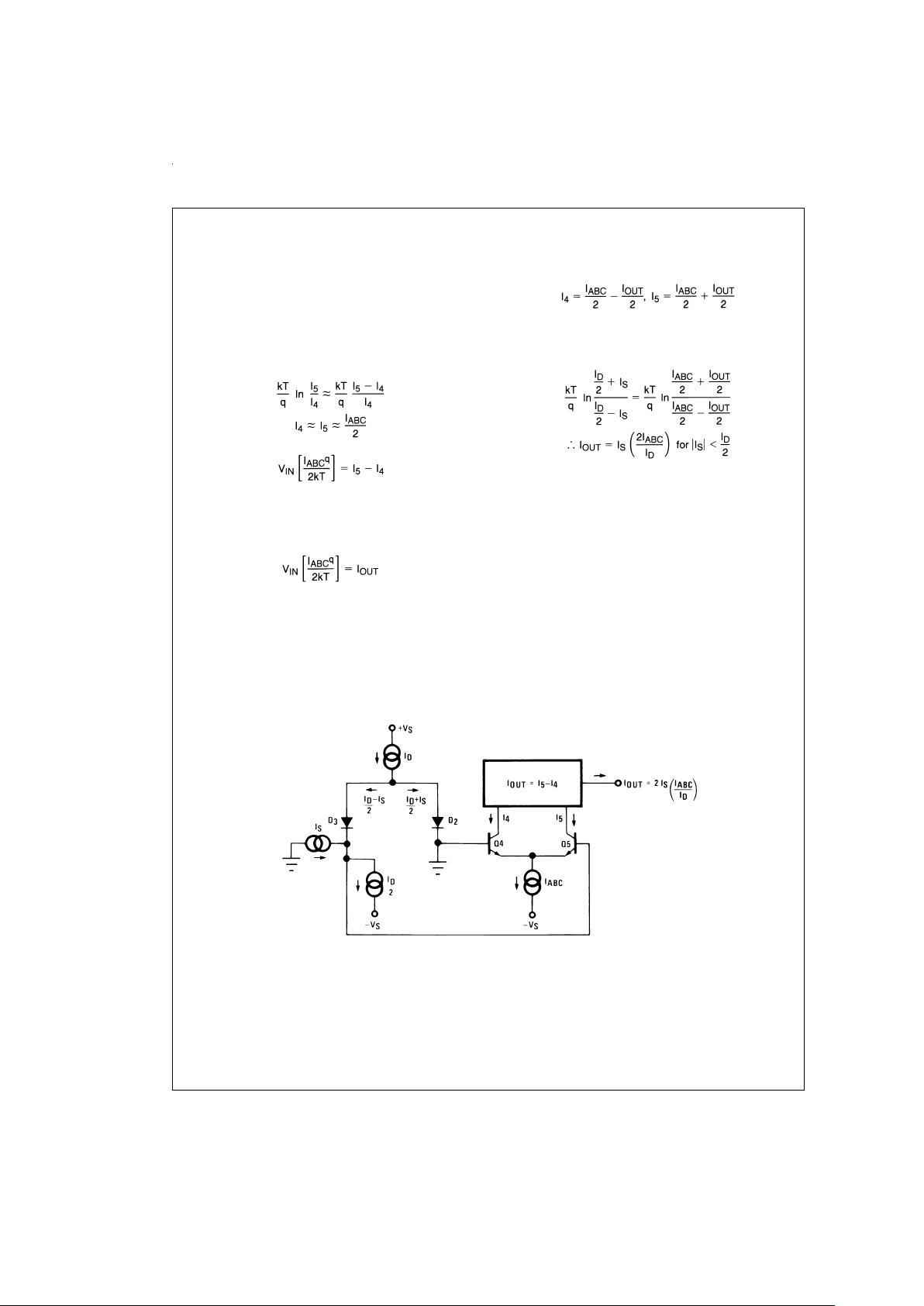
Figure 1
demonstrates how
the internal diodes can linearize the transfer function of the
amplifier. For convenience assume the diodes are biased
with current sources and the input signal is in the form of current I
S
. Since the sum of I4and I5is I
ABC
and the difference
is I
OUT
, currents I4and I5can be written as follows:
Since the diodes and the input transistors have identical geometries and are subject to similar voltages and temperatures, the following is true:
(6)
Notice that in deriving
Equation (6)
no approximations have
been made and there are no temperature-dependent terms.
The limitations are that the signal current not exceed I
D
/2
and that the diodes be biased with currents. In practice, replacing the current sources with resistorswill generate insignificant errors.
Applications:
Voltage Controlled Amplifiers
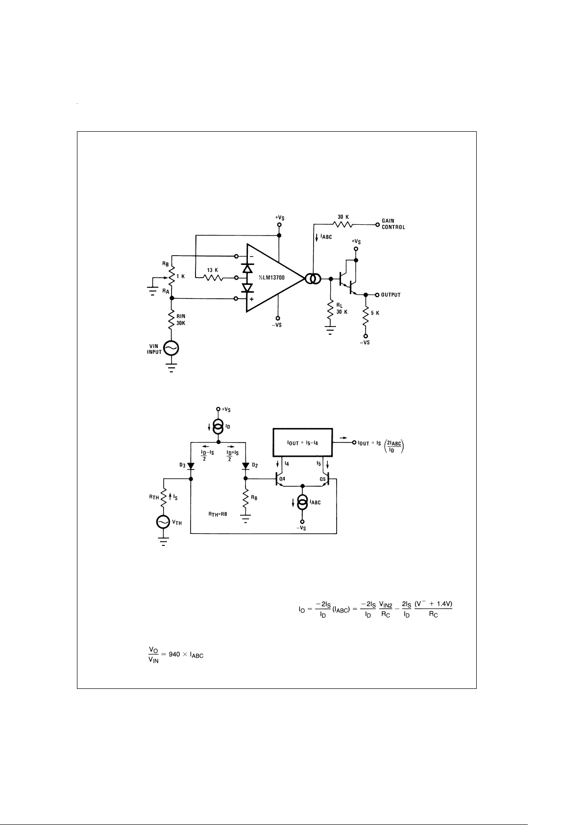
Figure 2
shows how the linearizing diodes can be used in a
voltage-controlled amplifier. To understand the input biasing,
it is best to consider the 13 kΩ resistor as a current source
and use a Thevenin equivalent circuit as shown in
Figure 3
.
This circuit is similar to
Figure 1
and operates the same. The
potentiometer in
Figure 2
is adjusted to minimize the effects
of the control signal at the output.
For optimum signal-to-noise performance, I
ABC
should be as
large as possible asshown bythe OutputVoltage vs. Amplifier Bias Current graph. Larger amplitudes of input signal
also improve the S/N ratio. The linearizing diodes help here
by allowing larger input signals for the same output distortion
as shown by the Distortion vs. Differential Input Voltage
graph. S/N may be optimized by adjusting the magnitude of
the input signal via R
IN
(
Figure 2
) until the output distortion is
below some desired level. The output voltage swing can
then be set at any level by selecting R
L
.
Although the noise contribution of the linearizing diodes is
negligible relative to the contribution of the amplifier’s internal transistors, I
D
should be as large as possible. This mini-
mizes the dynamic junction resistance of the diodes (r
e
) and
DS007981-8
FIGURE 1. Linearizing Diodes
www.national.com 6
Applications:
Voltage Controlled Amplifiers
(Continued)
maximizes their linearizing action when balanced against
R
IN
. A value of 1 mA is recommended for IDunless the spe-
cific application demands otherwise.
Stereo Volume Control
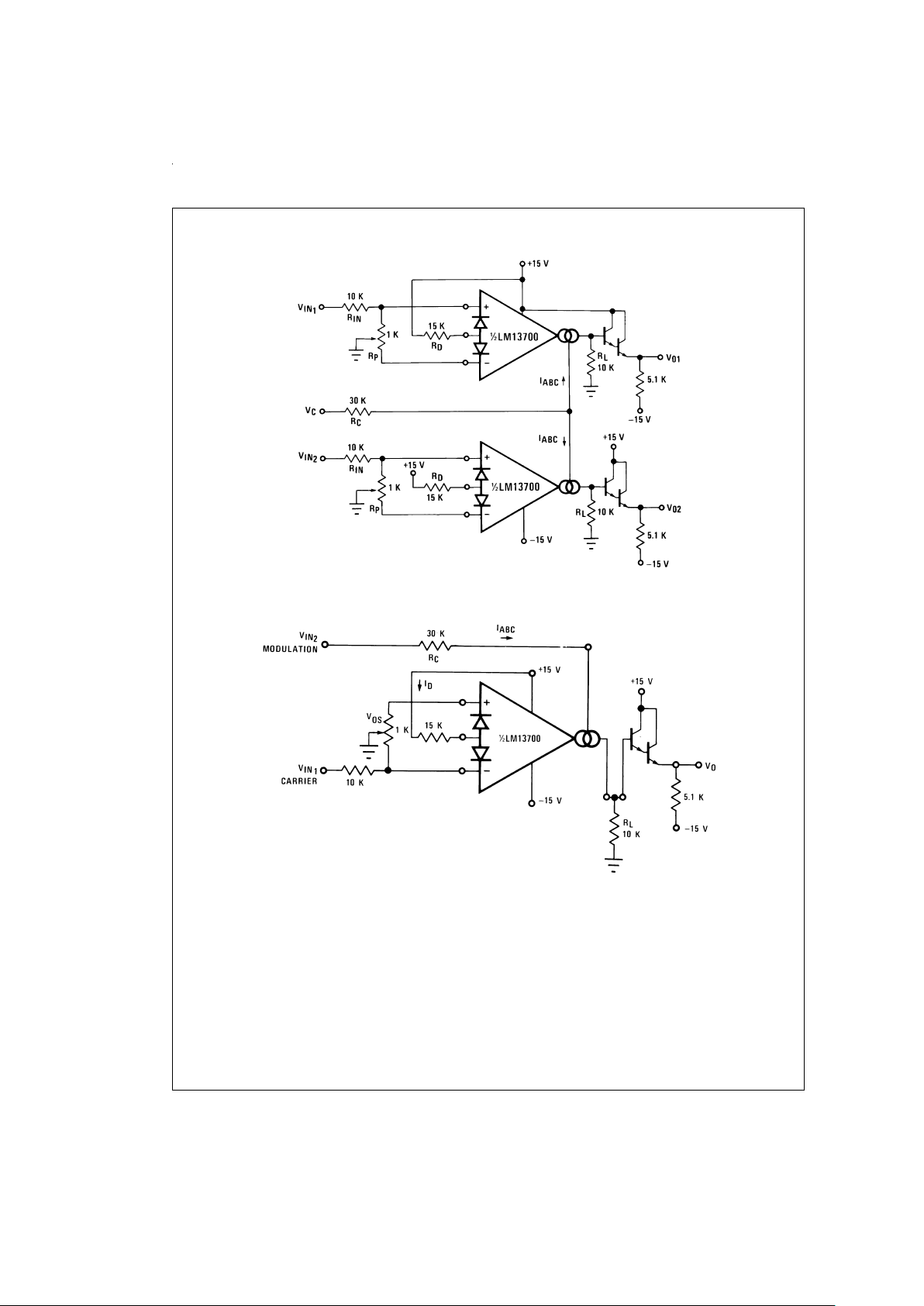
The circuit of
Figure 4
uses the excellent matching of the two
LM13700 amplifiers to provide aStereo Volume Control with
a typical channel-to-channel gain tracking of 0.3 dB. R
P
is
provided to minimize the output offset voltage and may be
replaced with two 510Ω resistors in AC-coupled applications.
For the component values given, amplifier gain is derivedfor
Figure 2
as being:
If VCis derived from a second signal source then the circuit
becomes an amplitude modulator or two-quadrant multiplier
as shown in
Figure 5
, where:
The constant term in the above equation may be cancelled
by feeding I
SxIDRC
/2(V− + 1.4V) into IO. The circuit of
Fig-
ure 6
adds RMto provide this current, resulting in a
four-quadrant multiplier where R
C
is trimmed such that V
O
=
0V for V
IN2
=
0V. R
M
also serves as the load resistor for IO.
DS007981-9
FIGURE 2. Voltage Controlled Amplifier
DS007981-10
FIGURE 3. Equivalent VCA Input Circuit
www.national.com7
Stereo Volume Control (Continued)
DS007981-11
FIGURE 4. Stereo Volume Control
DS007981-12
FIGURE 5. Amplitude Modulator
www.national.com 8
 Loading...