NSC JD54F399BFA Datasheet

TL/F/9533
54F/74F398
#
54F/74F399 Quad 2-Port Register
May 1995
54F/74F398#54F/74F399
Quad 2-Port Register
General Description
The ’F398 and ’F399 are the logical equivalents of a quad
2-input multiplexer feeding into four edge-triggered flipflops. A common Select input determines which of the two
4-bit words is accepted. The selected data enters the flipflops on the rising edge of the clock. The ’F399 is the 16-pin
version of the ’F398, with only the Q outputs of the flip-flops
available.
Features
Y
Select inputs from two data sources
Y
Fully positive edge-triggered operation
Y
Both true and complement outputsÐ’F398
Y
Guaranteed 4000V minimum ESD protectionÐ’F399
Commercial Military
Package
Package Description
Number
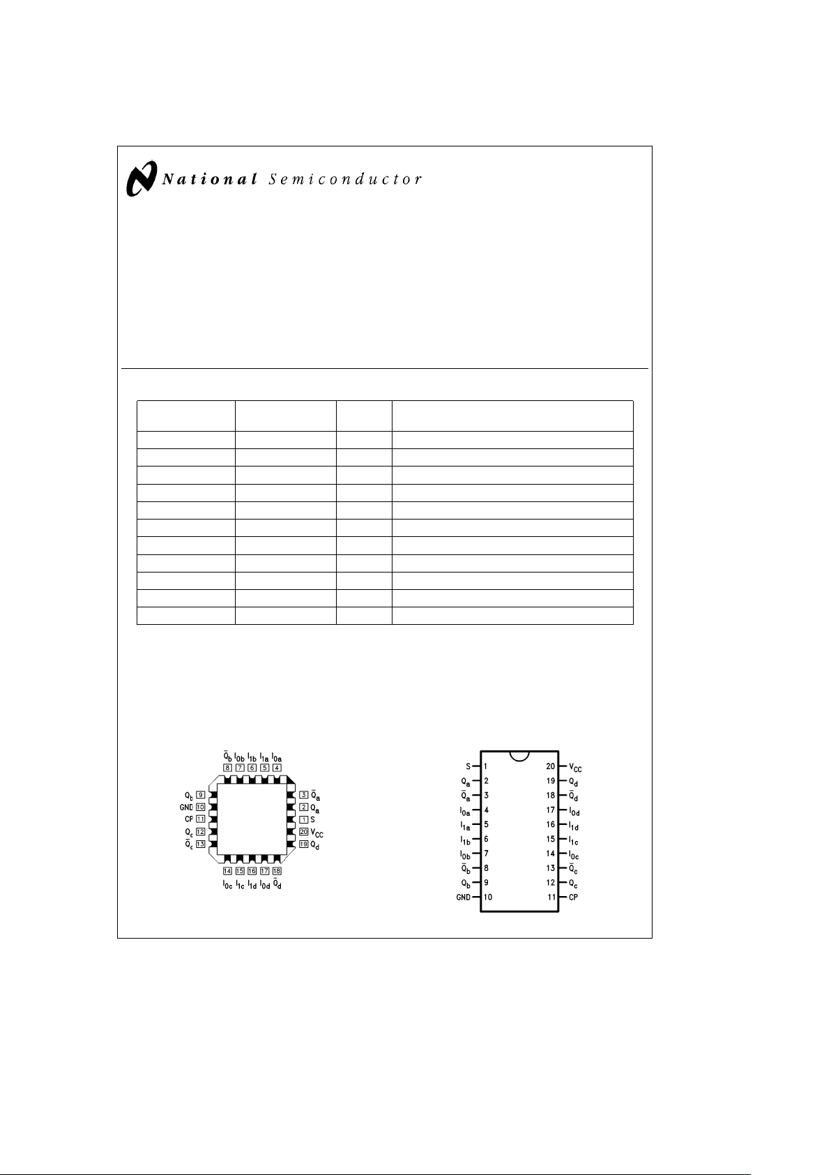
74F398PC N20A 20-Lead (0.300×Wide) Molded Dual-In-Line
54F398DM (Note 2) J20A 20-Lead Ceramic Dual-In-Line
74F398SC (Note 1) M20B 20-Lead (0.300×Wide) Molded Small Outline, JEDEC
54F398FM (Note 2) W20A 20-Lead Cerpack
54F398LM (Note 2) E20A 20-Lead Ceramic Leadless Chip Carrier, Type C
74F399PC N20A 20-Lead (0.300×Wide) Molded Dual-In-Line
54F399DM (Note 2) J20A 20-Lead Ceramic Dual-In-Line
74F399SC (Note 1) M20B 20-Lead (0.300×Wide) Molded Small Outline, JEDEC
74F399SJ (Note 1) M20D 20-Lead (0.300×Wide) Molded Small Outline, EIAJ
54F399FM (Note 2) W20A 20-Lead Cerpack
54F399LM (Note 2) E20A 20-Lead Ceramic Leadless Chip Carrier, Type C
Note 1: Devices also available in 13×reel. Use suffixeSCX and SJX.
Note 2: Military grade device with environmental and burn-in processing. Use suffix
e
DMQB, FMQB and LMQB.
Connection Diagrams
’F398
Pin Assignment
for LCC
TL/F/9533– 5
Pin Assignment
for DIP, SOIC and Flatpak
TL/F/9533– 6
TRI-STATEÉis a registered trademark of National Semiconductor Corporation.
C
1995 National Semiconductor Corporation RRD-B30M75/Printed in U. S. A.

Connection Diagrams (Continued)
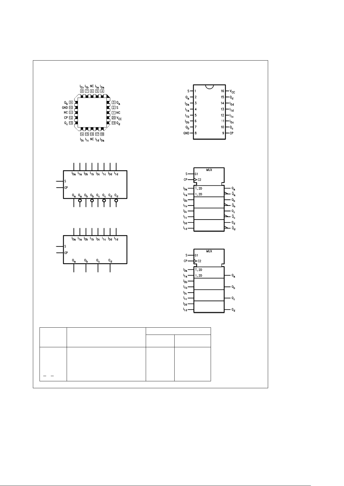
’F399
TL/F/9533– 7
TL/F/9533– 8
Logic Symbols
’F398
TL/F/9533– 2
’F399
TL/F/9533– 4
IEEE/IEC
’F398
TL/F/9533– 1
’F399
TL/F/9533– 3
Unit Loading/Fan Out
54F/74F
Pin Names Description
U.L. Input I
IH/IIL
HIGH/LOW Output IOH/I
OL
S Common Select Input 1.0/1.0 20 mA/b0.6 mA
CP Clock Pulse Input (Active Rising Edge) 1.0/1.0 20 mA/
b
0.6 mA
I
0a–I0d
Data Inputs from Source 0 1.0/1.0 20 mA/b0.6 mA
I1a–I
1d
Data Inputs from Source 1 1.0/1.0 20 mA/b0.6 mA
Q
a–Qd
Register True Outputs 50/33.3
b
1 mA/20 mA
Qa–Q
d
Register Complementary Outputs (’F398) 50/33.3
b
1 mA/20 mA
2

Functional Description
The ’F398 and ’F399 are high-speed quad 2-port registers.
They select four bits of data from either of two sources
(Ports) under control of a common Select input (S). The
selected data is transferred to a 4-bit output register synchronous with the LOW-to-HIGH transition of the Clock input (CP). The 4-bit D-type output register is fully edge-triggered. The Data inputs (I
0x,I1x
) and Select input (S) must be
stable only a setup time prior to and hold time after the
LOW-to-HIGH transition of the Clock input for predictable
operation. The ’F398 has both Q and Q
outputs.
Function Table
Inputs Outputs
SI
0
I
1
QQ*
IIXLH
IhXH L
hX I L H
hXhH L
H
e
HIGH Voltage Level
L
e
LOW Voltage Level
h
e
HIGH Voltage Level one setup time prior to the LOW-to-HIGH clock
transition
I
e
LOW Voltage Level one setup time prior to the LOW-to-HIGH clock
transition
X
e
Immaterial
*’F398 only
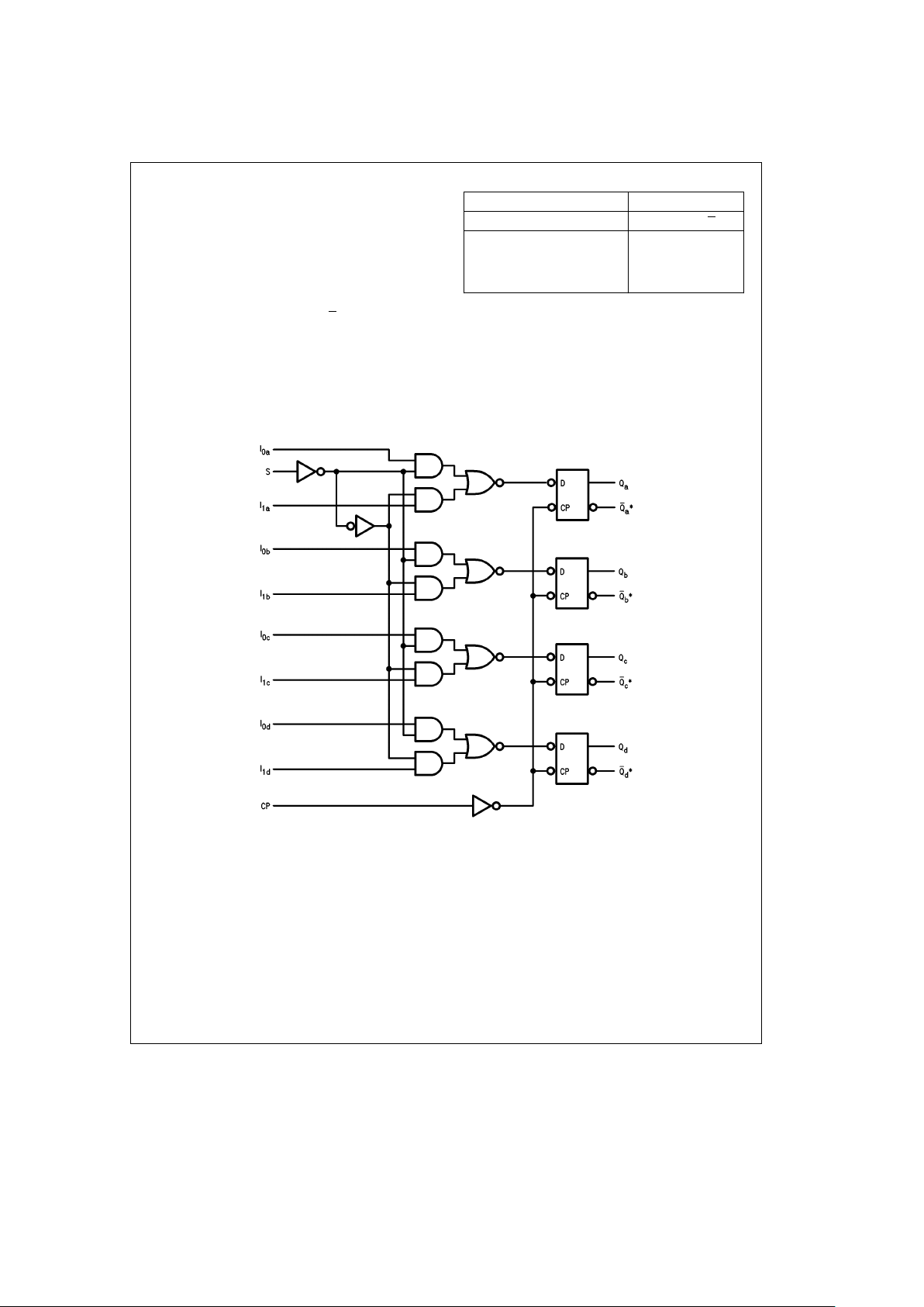
Logic Diagram
TL/F/9533– 9
*’F398 Only
Please note that this diagram is provided only for the understanding of logic operations and should not be used to estimate propagation delays.
3
 Loading...