NSC ICSS1002VJE, ICSS1001 Datasheet
TL/DD11727
ICSS1001, ICSS1002, and ICSS1003 IC/SS Power Line Carrier Local Area Network Chip Set
PRELIMINARY
February 1995
ICSS1001, ICSS1002, and ICSS1003
IC/SS Power Line Carrier
Local Area Network Chip Set
General Description
Integrated Circuit/Spread Spectrum (IC/SSTM) is a power
line carrier local area network system implemented in a
three chip solution, using power line carrier technology developed by Itron and Cyplex. It is designed to operate with
high reliability over the full range of power line conditions.
IC/SS is offered with an integral local area network protocol, designed specifically for supervisory control and data
acquisition applications.
Features
Y
Spread spectrum, adaptive frequency hopping modulation provides high immunity to power line noise.
Y
Network/transparent option offers the user the ability to
carry proprietary protocols transparently, or to use the
built-in link layer protocol.
Y
A very flexible interface to the user’s circuit is provided,
configurable either to accept serial data or to accept
data from an 8-bit parallel bus. Handshake lines are
provided to facilitate interface to common microprocessors in parallel mode.
Y
When used with the specified coupling networks, the
modem operates in conformance with both the
CENELEC standard for electric utility application
(9 kHz–95 kHz), and with FCC Class A requirements.
Y
Data rate is variable, based on line conditions, from
300 bps to 3200 bps.
Y
When used with the specified coupling networks, the
system provides 93 dB of dynamic range, appropriate
for line loading and attenuation effects common on
power lines.
Y
The modem’s bit error rate performance in additive
white noise approaches the theoretical maximum, and
in addition it provides excellent immunity to the impulsive noise characteristic of power lines.
Applications
Y
Automated meter reading (AMR)
Y
Demand side management
Y
Distribution automation
Y
Environmental control systems
Y
Other power line carrier applications requiring high
reliability
Block Diagram
TL/DD/11727– 1
TRI-STATEÉis a registered trademark of National Semiconductor Corporation.
MICROWIRE
TM
and WATCHDOGTMare trademarks of National Semiconductor Corporation.
IC/SS
TM
is a trademark of Cyplex.
C
1995 National Semiconductor Corporation RRD-B30M105/Printed in U. S. A.
Modem Operation
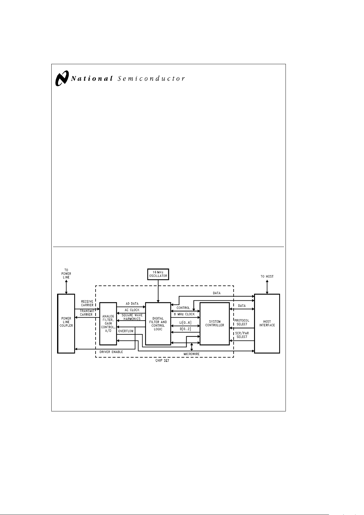
A block diagram of the modem is shown on page 1. It includes four major elements:
1. Coupling network to the power line.
2. Analog filter, gain control, and A/D.
3. Digital filter and control logic.
4. System controller.
Each of these is described in more detail below.
COUPLING NETWORK
The coupling network provides protection against the AC
power line 60 Hz/50 Hz energy, and initial filtering of power
line noise. It provides a match of impedances to the power
line, and also contains a power amplification stage for the
transmitter. A variety of coupling networks are available
from Cyplex, suitable for:
220 VAC ungrounded operation (meters and 220 VAC
load control).
110 VAC/neutral operation (110 VAC load control).
Three-terminal operation (intended for gateways and
master units which must communicate with both of the
above).
The coupling networks require
g
5V power, ground, and in-
terface to the analog section of the system.
ICSS1001ÐController
The controller provides the adaptive frequency hopping, the
user interface, and link layer protocol.
ICSS1002ÐDigital Chip
The digital section of the system provides additional receive
filtering and received signal detection functions. It generates
the necessary internal clocks and interface signals to the
microcontroller.
ICSS1003ÐAnalog Chip
The analog section of the system provides receive signal
filtering, and also generates the transmit carrier based on
control and clock signals from the digital section.
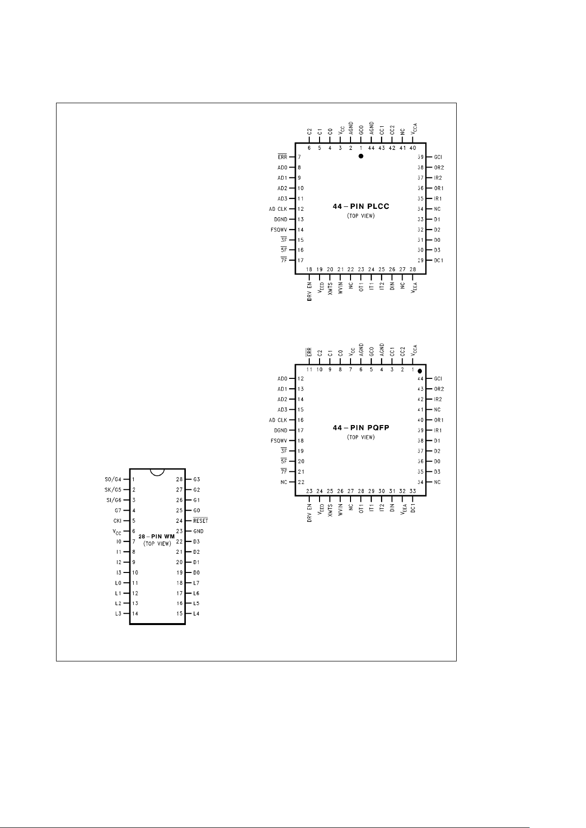
Connection Diagrams
TL/DD/11727– 2
Wide Molded Small Outline Package (WM)
Order Number ICSS1001WM
NS Package Number M28B
TL/DD/11727– 4
Plastic Leaded Chip Carrier (PLCC)
Order Number ICSS1003V
NS Package Number V44A
TL/DD/11727– 28
Plastic Quad Flatpak (PQFP)
Order Number ICSS1003VGZ
NS Package Number VGZ44A
2
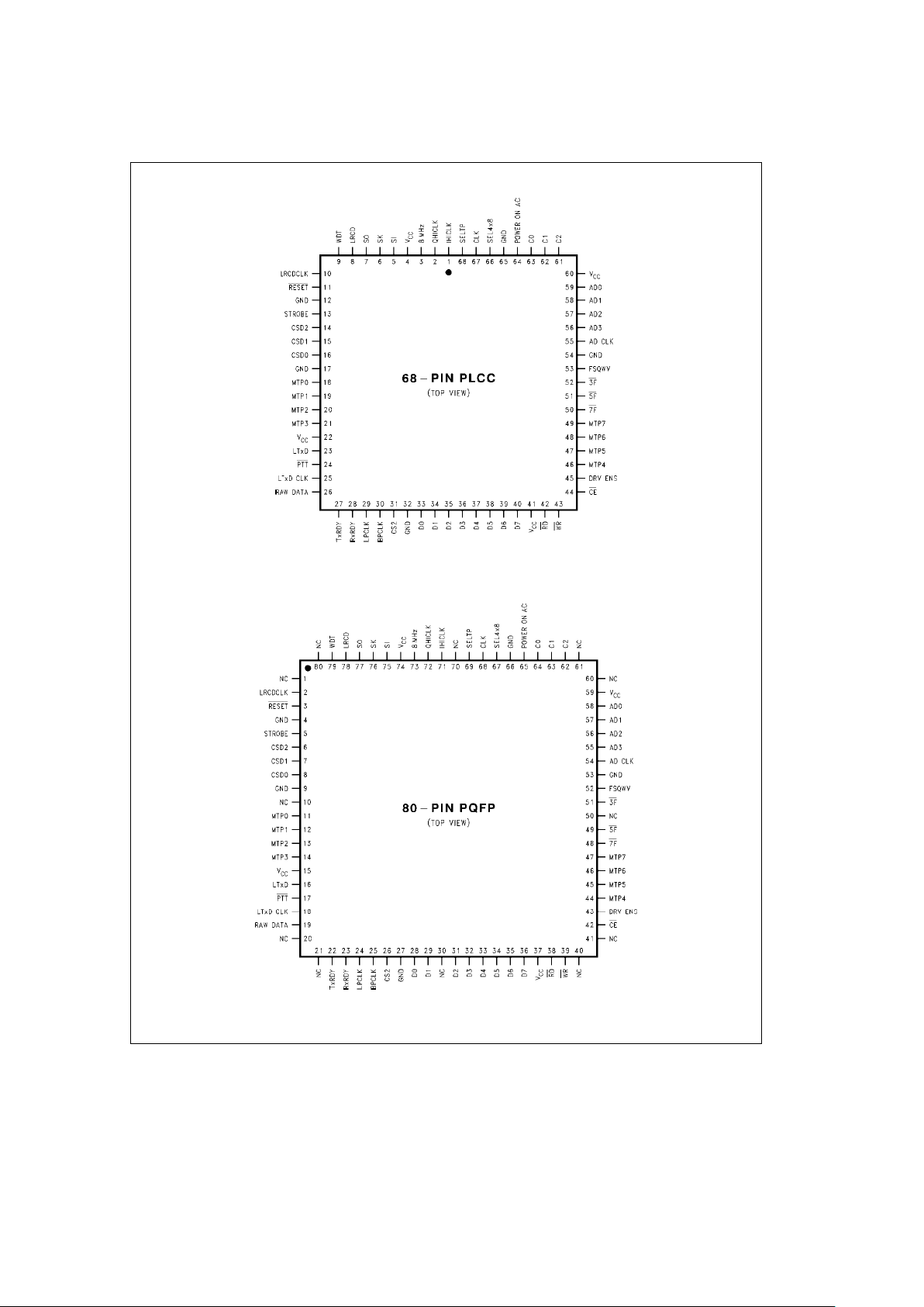
Connection Diagrams (Continued)
TL/DD/11727– 3
Plastic Leaded Chip Carrier (PLCC)
Order Number ICSS1002V4
NS Package Number V68A
TL/DD/11727– 27
Plastic Quad Flatpak (PQFP)
Order Number ICSS1002VJE
NS Package Number VJE80B
3
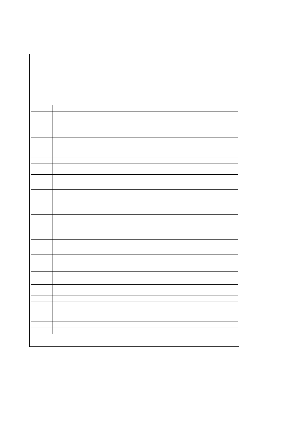
Pin Descriptions
Tables I, II and III describe the various pins that are used for
external connections outside of the chip set. These pins are
shown in the Connection Diagrams.
Type One of the following:
I Input
O Output
T TRI-STATE
É
P Power
Function A brief description of each signal’s function.
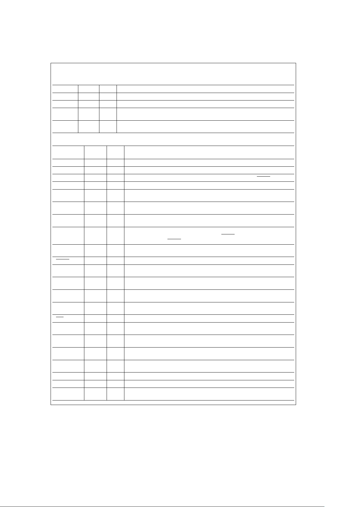
TABLE I. ICSS1001 Pin Descriptions
Pin Name Pin No. Type Function
SO/G4 1 O MICROWIRETMSO to digital ASIC
SK/G5 2 O MICROWIRE clock to digital ASIC
SI/G6 3 I MICROWIRE SI from digital ASIC
G7 4 O Overflow of A/D converter from analog ASIC
CKI 5 l 8 MHz clock input from digital ASIC
V
CC
6 P Input power
I0 7 I RAW DATA input from digital ASIC
I1 8 O RxRDY handshake line for parallel port
I2 9 I SER/PAR-input read after reset determines whether firmware will use serial or parallel host
port. HIGH
e
serial
I3 10 I NET/TRN-input read continuously. If HIGH and serial port is selected commands are
processed; if LOW, all received characters are treated as transparent data. If parallel port is
selected, this pin has no effect.
L0 11 I RTS flow control from host. If serial port is selected (pin 9eHIGH), LOW enables output of
data on RCD and HIGH prevents output on RCD. A byte in the process of being output when
RTS goes HIGH will be completed. RTS has no effect if parallel port is selected.
If parallel is selected (pin 9
e
LOW), COMMAND HIGH denotes the presence of a command
in the parallel port input buffer. LOW denotes the presence of data.
L1 12 O CTS flow control to host. Normally LOW. If serial port is selected (pin 9eHIGH) then HIGH
indicates host should not send data to TXD. A maximum of three bytes will be accepted after a
transition from LOW to HIGH.
If parallel port is selected (pin 9
e
LOW), then STATUS HIGH denotes that the byte available
for the host to read is a status code. A LOW denotes that the available byte is data.
L2 13 O RCD receive data output to host, in byte asynchronous format, 8 data bits, parity one start and
one stop bit. Active baud rate and parity default is 1200 baud, no parity. Other settings may be
selected by DIP switch. Active only if serial port is selected.
L3 14 I TXD transmit data input from host
L4 15 O LTXD CLK serial data clock for data to be transmitted by the digital ASIC, not Manchester-
encoded
L5 16 O TxRDY handshake line for parallel port
L6 17 O PTT Active LOW places digital chip in transmit mode
L7 18 O LTXD serial data to be transmitted by digital ASIC, not Manchester-encoded. Active HIGH.
ASIC Manchester-encodes the data using LTXD CLK.
D0 19 O CSD digital ASIC internal MlCROWIRE register address selection
D1 20 O CSD1 digital ASIC internal MlCROWIRE register address selection
D2 21 O CSD2 digital ASIC internal MICROWIRE register address selection
D3 22 O STROBE MICROWIRE output to digital ASIC
GROUND 23 P Ground
RESET 24 I RESET from digital chip
4
Pin Descriptions (Continued)
TABLE I. ICSS1001 Pin Descriptions (Continued)
Pin Name Pin No. Type Function
G0 25 I LRCD CLK recovered clock from demodulated data input from digital ASlC
G1 26 No connection
G2 27 I LRCD recovered data from demodulated data input from digital ASIC, after Manchester
decoding
G3 28 O WDT firmware outputs a square wave to digital chip, maintaining a one-shot. If WDT output
stops, digital ASIC will force a system reset on pin 24.
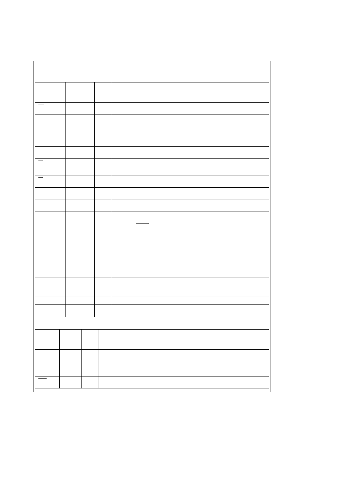
TABLE II. ICSS1002 Pin Descriptions
Pin Name
Pin No.
Type Function
(V Pkg.)
IHICLK 1 O Output Test Point: A test point.
QHICLK 2 O Output Test Point: A test point.
8 MHz 3 O 8 MHz Output: This is the CLK divided by 2. This output goes low while RESET is LOW.
SI 5 T MICROWIRE Serial Input: This pin drives the MICROWIRE SI Input on the controller.
SK 6 T MICROWIRE Shift Clock: This pin accepts the MICROWIRE shift clock to the Controller
interface on the IC/SS digital ASIC.
SO 7 T MICROWIRE Serial Output: This pin accepts the MICROWIRE serial data to the
Controller interface on the IC/SS digital ASIC.
LRCD 8 O Recovered Data: This is the serial data received from the power line after Manchester
decoding.
WDT 9 T WATCHDOGTMTimer Disable: This input from the controller keeps the digital ASIC
active. If it goes away, the digital ASlC will generate RESET
pulse after the WATCHDOG
timers times out. This RESET
pulse will reset the entire PLC chip set.
LRCDCLK 10 O Recovered Clock: This is the clock received from the power line after Manchester
decoding.
RESET 11 I Reset: Active LOW reset for the entire IC/SS chip set.
STROBE 13 T MICROWIRE Strobe input: This pin accepts the MICROWIRE strobe to the controller
interface on the IC/SS digital ASIC.
CSD2–CSD0 14–16 T Controller Interface Mode Select: These inputs are used to select the operation modes
of the controller interface circuitry on the IC/SS digital ASIC.
MTP0–MTP3 18– 21 O Test Points: These output pins provide access to one of the filter outputs on the detector
integration bus.
LTXD 23 O Serial Data to be transmitted: This input is the serial data to be transmitted. It is not
Manchester encoded.
PTT 24 T Push to talk: This is an active low signal that puts the digital ASIC into the transmit mode.
LTXD CLK 25 T Serial Data Transmit Clock: This input is the clock for the serial data (LTXD) that is used
to Manchester encode the data prior to transmission.
RAW DATA 26 O Raw Data: This output is the raw data received by the IC/SS circuit after de-multiplex prior
to Manchester decode.
TxRDY 27 O Transmit Data Ready: When this signal is HIGH the parallel port is ready to accept a new
byte from the user data bus.
RxRDY 28 O Receive Data Ready: When this signal is HIGH there is a byte available in the parallel
port to be read by the user data bus.
LPCLK 29 O LPCLK: This is an internal test point.
BPCLK 30 O BPCLK: This is an internal test point.
CS2 31 O Chip Select: This is the MICROWIRE chip select output. It is used to enable read/write of
external MICROWIRE data ports.
5
Pin Descriptions (Continued)
TABLE II. ICSS1002 Pin Descriptions (Continued)
Pin Name
Pin No
Type Function
(V Pkg.)
D0–D7 33–40 I/O Data Bus: This is the parallel port data bus.
RD 42 T Read: This is the parallel port read control. Used with Chip Enable it allows the
parallel port to be read.
WR 43 T Write: This is the parallel port write control. Used with Chip Enable it allows the
parallel port to be written.
CE 44 T Chip Enable: This is the parallel port enable to read or write. It is active low.
DRV EN 45 O Drive Enable: This is the transmit enable signal used by the Analog chip to disable
the receiver mode and enable the transmitter mode
MTP4–MTP7 46–49 O Test Points: These output pins provide access to one of the filter outputs of the
detector integration bus
7F 50 O Seventh Harmonic Overtone Cancellation Signal: This is the seventh harmonic
overtone cancellation signal used to convert FSQWV to a sine wave in the Analog
chip D/A
5F 51 O Fifth Harmonic Overtone Cancellation Signal: This is the fifth harmonic overtone
cancellation signal used to convert FSQWV to a sine wave in the Analog chip D/A
3F 52 O Third Harmonic Overtone Cancellation Signal: This is the Third harmonic overtone
cancellation signal used to convert FSQWV to a sine wave in the Analog chip D/A
FSQWV 53 O Square Wave Transmit Signal: This is the Manchester-encoded frequency mixed
signal, ready for transmission to the power line
AD CLK 55 O A/D Clock: This is the clock for the Analog chip AID converter. It is used to latch the
AD output. It is the A/D sample rate. This is the CLK divided by 16. This output goes
HIGH while RESET
is LOW.
AD3–AD0 56 – 59 T Received Data: These pins are the digital four bit bus from the Analog chip which
contains the ones complement A/D converted signal from the power line
C2–C0 61–63 O Analog Gain Control: These signals are used to set the gain of the Analog chip gain
controlled amplifier
Power on AC 64 O Power on Reset RC Node: This is the power on reset Resistor/Capacitor connect
point. An external RC network charges up to the gate threshold to release the RESET
signal. When this pin is LOW the RESET is active.
SEL4X8 66 T Select 4X or 8X: This is the select line used to set the digital filter clock sample rate
CLK 67 T Clock: This is the 16 MHz clock input
SEL TP 68 T Select Test Points: This signal selects which internal nodes are brought out on the
Test Point Bus and whether Raw Data is inverted or not
V
CC
4, 22, 41, 60 P VCC: These are positive voltage power supply pins to the part
GND 12, 17, 32, P GND: These are the negative (or 0V) power supply pins to the part
54, 65
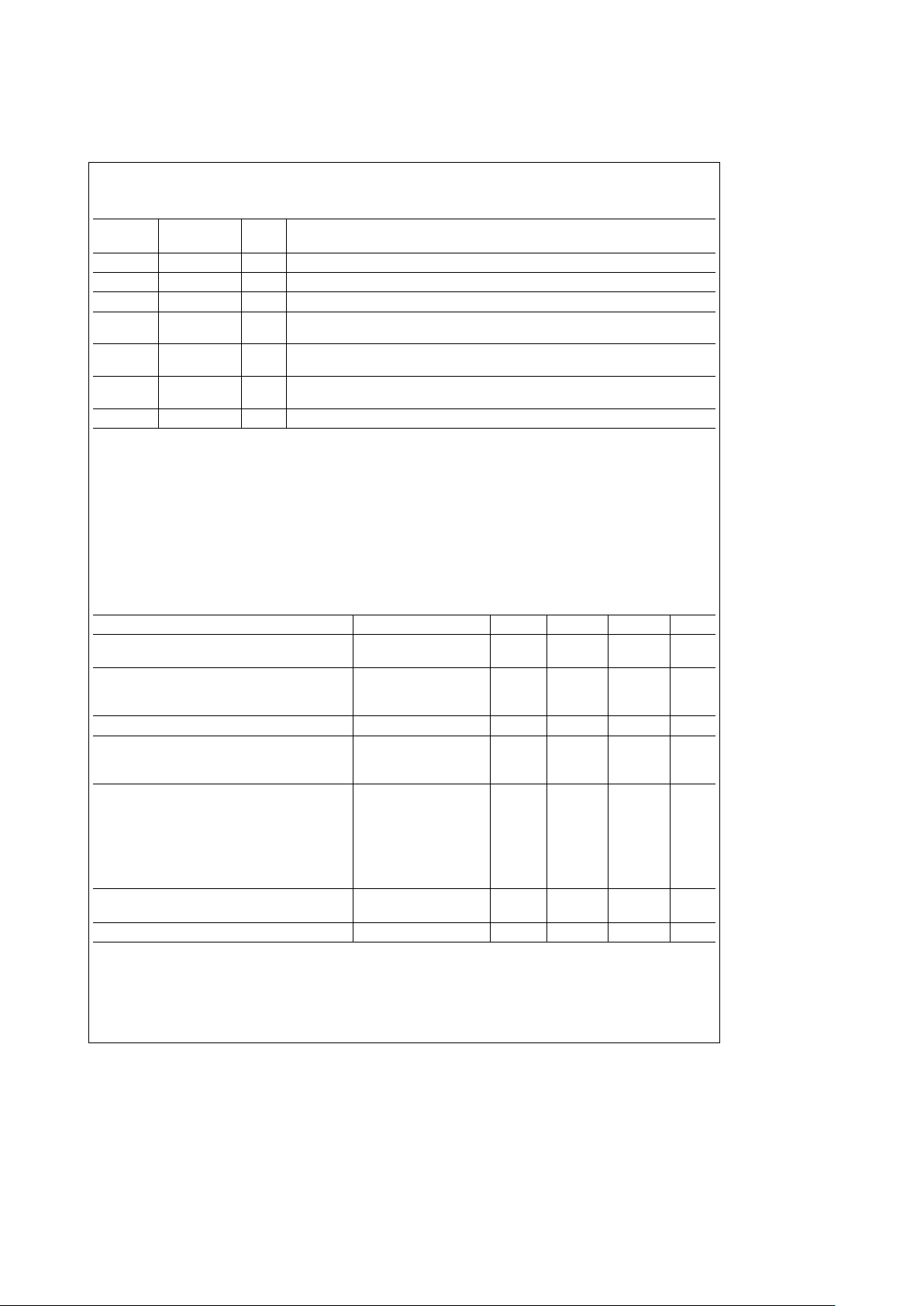
TABLE III. ICSS1003 Pin Descriptions
Pin Name
Pin No.
Type Function
(V Pkg.)
GCO 1 Gain Control Amplifier Test Point: A test point to monitor the gain of the gain amplifier
AGND 2 P Analog Ground: The ground reference pin for the gain control amplifier
V
CC
3PDigital Positive Power Supply Pin: The VCCpin for the digital portion of the ASIC
C0–C2 4–6 I Gain Control Amplifier Gain Setting: These pins set the gain of the gain control amplifier.
These signals are generated by the digital ASIC.
ERR 7OA/D Overflow Signal: This signal goes HIGH if the Analog signal from the gain control
amplifier to the Analog to Digital Converter is being clipped by the A/D converter
6

Pin Descriptions (Continued)
TABLE III. ICSS1003 Pin Descriptions (Continued)
Pin Name
Pin No.
Type Function
(V Pkg.)
AD0–AD3 8 – 11 O A/D Digital Output: These signals are the ones complement digital output of the signal
received from the power line. It is the output of the flash A/D sampled at the AD CLK rate.
AD CLK 12 I Clock For The Flash A/D Converter: This is the clock used by the A/D converter to sample
the signal received from the power line. It is normally 1 MHz and is generated by the digital
ASIC.
DGND 13 P Digital Ground Power Supply Pin: This is the ground (0V) power supply for the digital
portion of the ASIC
FSQWV 14 I Square Wave Transmit Signal: This is the Manchester-encoded, frequency mixed signal
3F 15 I Third Harmonic Overtone Cancellation Signal: This is the third harmonic overtone
cancellation signal used to convert FSQWV to a sine wave in the Analog chip D/A
5F 16 I Fifth Harmonic: Overtone Cancellation Signal: This is the fifth harmonic overtone
cancellation signal used to convert FSQWV to a sine wave in the Analog chip D/A
7F 17 I Seventh Harmonic: Overtone Cancellation Signal: This is the seventh harmonic overtone
cancellation signal used to convert FSQWV to a sine wave in the Analog chip D/A
DRV EN 18 I Drive Enable: This is the transmit enable signal used by the Analog chip to disable the
receiver mode and enable the transmitter mode
VEED 19 P Digital Negative Power Supply Pin: This is the negative (b5V) power supply for the digital
portion of the ASIC
XMTS 20 O Digital To Analog Converter Integrator Output: This is the analog output of the D/A
converter integrator
WVIN 21 Digital To Analog Converter Integrator Input: This is the analog input of the D/A converter
integrator. It is connected internally to the D/A converter output. It is used to connect the
external integrator capacitor to the integrator input.
OT1 23 O Amplifier Output: Buffer amplifier between the D/A converter and the power driver amplifier
output
IT1 24 I Amplifier Positive Input: Buffer amplifier between the D/A converter and the power driver
amplifier positive input
IT2 25 I Amplifier Negative Input: Buffer amplifier between the D/A converter and the power driver
amplifier negative input
DIN 26 I Power Amplifier Input: This is the power amplifier input
VEEA 28 P Analog Negative Power Supply Pin: This is the negative (b5V) power supply for the analog
portion of the ASIC
DC1 29 O Power Amplifier Divided Input: This is the power amplifier resistor divided input
D3 30 I Power Amplifier Feedback Input: This is one of the switched power amplifier feedback
points
D0 31 I Power Amplifier Feedback Input: This is one of the switched power amplifier feedback
points
D2 32 O Power Amplifier Negative Output: This is the power amplifier negative output driver output
D1 33 O Power Amplifier Positive Output: This is the power amplifier positive output driver output
IR1 35 O Unity Gain Amplifier Input: First stage receiver filter input
OR1 36 O Unity Gain Amplifier Output: First stage receiver filter output
IR2 37 I Unity Gain Amplifier Input: Second stage receiver filter input
7
Pin Descriptions (Continued)
TABLE III. ICSS1003 Pin Descriptions (Continued)
Pin Name
Pin No.
Type Function
(V Pkg.)
IR2 38 O Unity Gain Amplifier Output: Second stage receiver filter output
GCI 39 I Gain Control Amplifier Input: This is the gain control amplifier input
VCCA40PAnalog Positive Power Supply Pin: The VCCpin for the analog portion of the ASIC
CC2 42 Gain Control Amplifier Offset Compensation Input: This is the gain control amplifier
offset compensation input capacitor connect point
CC1 43 Gain Control Amplifier Offset Compensation Output: This is the gain control
amplifier offset compensation output capacitor connect point
AGND 44 Analog Gain Control: This is the ground (0V) power supply for the analog portion of the
ASIC
NC 22, 27, 34, 41 No Connect: These pins are not connected
Absolute Maximum Ratings
If Military/Aerospace specified devices are required,
please contact the National Semiconductor Sales
Office/Distributors for availability and specifications.
Supply Voltage 7V
Total Current into V
CC
Pin (Source) 100 mA
Total Current out of GND Pin (Sink) 110 mA
Storage Temperature Range
b
65§Ctoa150§C
Note:
Absolute maximum ratings indicate limits beyond
which damage to the device may occur. DC and AC electrical specifications are not ensured when operating the device at absolute maximum ratings.
ICSS1001 DC Electrical Characteristics (
b
40§CsT
A
s
a
85§C)
Parameter Conditions Min Typ Max Units
Operating Voltage Power Supply Ripple (Note 1) 2.5 5.5
V
Peak to Peak 0.1 V
CC
Supply Current
CKI
e
10 MHz (Note 2) V
CC
e
6V, t
C
e
1 ms15
mA
CKI
e
4 MHz V
CC
e
2.5V, t
C
e
2.5 ms2
HALT (Note 3) V
CC
e
6V, CKIe0 MHz
k
110mA
IDLE
CKI
e
10 MHz V
CC
e
6V, t
C
e
1 ms 2.2 mA
CKI
e
4 MHz V
CC
e
2.5V, t
C
e
2.5 ms 0.6 mA
Input Levels (VIH,VIL)
Reset, CKI
V
Logic HIGH 0.8 V
CC
Logic LOW 0.2 V
CC
All Other Inputs
Logic HIGH 0.7 V
CC
Logic LOW 0.2 V
CC
Hi-Z Input Leakage Input Pull-Up Current V
CC
e
6V
b
2
a
2
mA
V
CC
e
6V, V
IN
e
0V 40 250
G Port Input Hysteresis (Note 6) 0.05 V
CC
0.35 V
CC
V
8
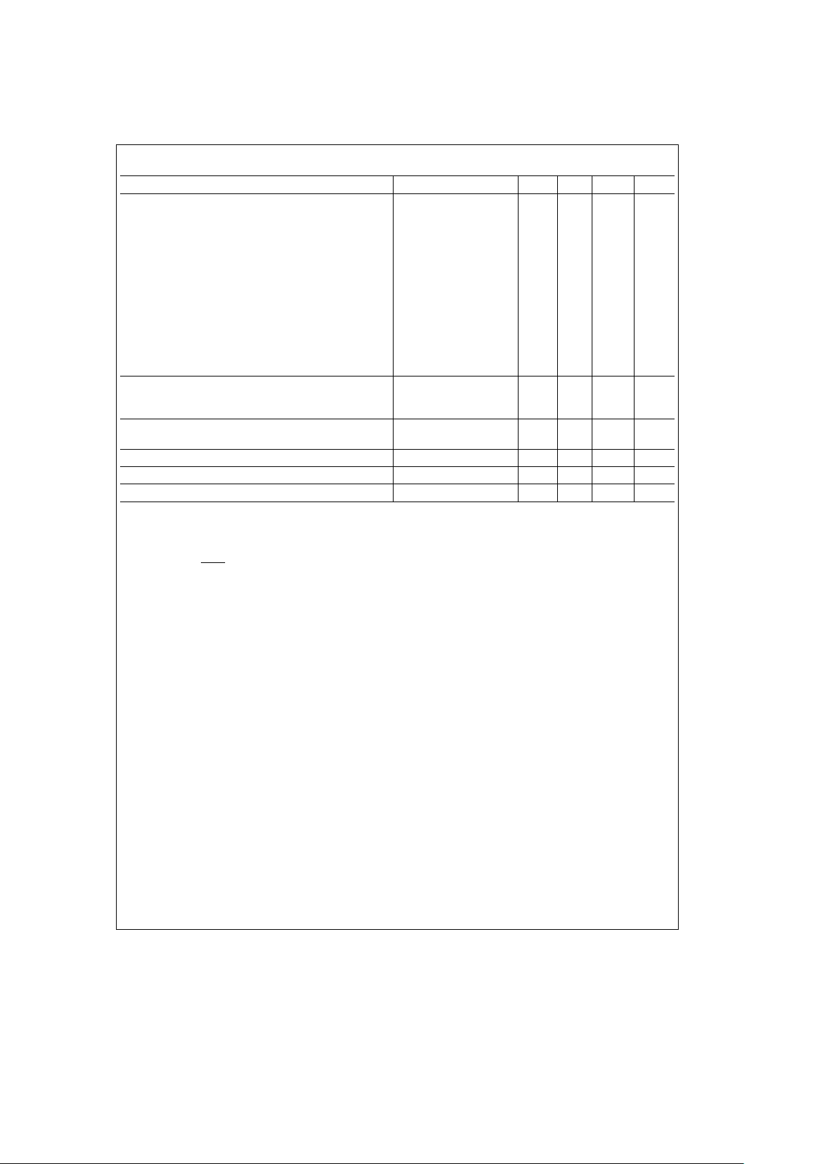
ICSS1001 DC Electrical Characteristics (
b
40§CsT
A
s
a
85§C) (Continued)
Parameter Conditions Min Typ Max Units
Output Current Levels
D Outputs
Source V
CC
e
4.0V, V
OH
e
3.3V 0.4 mA
V
CC
e
2.5V, V
OH
e
1.8V 0.2 mA
Sink V
CC
e
4.0V, V
OL
e
1.0V 10 mA
V
CC
e
2.5V, V
OL
e
0.4V 0.2 mA
All Others
Source (Weak Pull-Up) V
CC
e
4.0V, V
OH
e
2.7V 10 110 mA
V
CC
e
2.5V, V
OH
e
1.8V 2.5 33 mA
Source (Push-Pull) V
CC
e
4.0V, V
OH
e
3.3V 0.4 mA
V
CC
e
2.5V, V
OH
e
1.8V 0.2 mA
Sink (Push-Pull) V
CC
e
4.0V, V
OL
e
0.4V 1.6 mA
V
CC
e
2.5V, V
OL
e
0.4V 0.7 mA
TRI-STATE Leakage V
CC
e
6.0V
b
2.0
a
2.0 mA
Allowable Sink/Source Current per Pin
D Outputs (Sink) 15
mA
All Other 3
Maximum Input Current without Latchup Room Temp
g
100 mA
(Notes 4, 6)
RAM Retention Voltage, VR(Note 5) 500 ns Rise and Fall Time 2.0 V
Input Capacitance (Note 6) 7 pF
Load Capacitance (Note 6) 1000 pF
Note 1: Maximum rate of voltage change must be less than 0.5V/ms.
Note 2: Supply current is measured after running 2000 cycles with a square wave CKI input, CKO open, inputs at rails, and outputs open.
Note 3: The HALT mode will stop CKI from oscillating in the RC and the Crystal configurations. HALT test conditions: all inputs tied to V
CC
; L and G port I/Os
configured as outputs and programmed low; D outputs programmed low. Parameter refers to HALT mode entered via setting bit 7 of the G Port data register. Part
will pull up CKI during HALT in crystal clock mode.
Note 4: Pins G6 and RESET
are designed with a high voltage input network. These pins allow input voltages greater than VCCand the pins will have sink current to
V
CC
when biased at voltages greater than VCC(the pins do not have source current when biased at a voltage below VCC). The effective resistance to VCCis 750X
(typical). These two pins will not latch up. The voltage at the pins must be limited to less than 14V. Voltages in excess of 14V will cause damage to the pins. This
excludes ESD transients.
Note 5: Condition and parameter valid only for part in HALT mode.
Note 6: Parameter characterized but not tested.
9
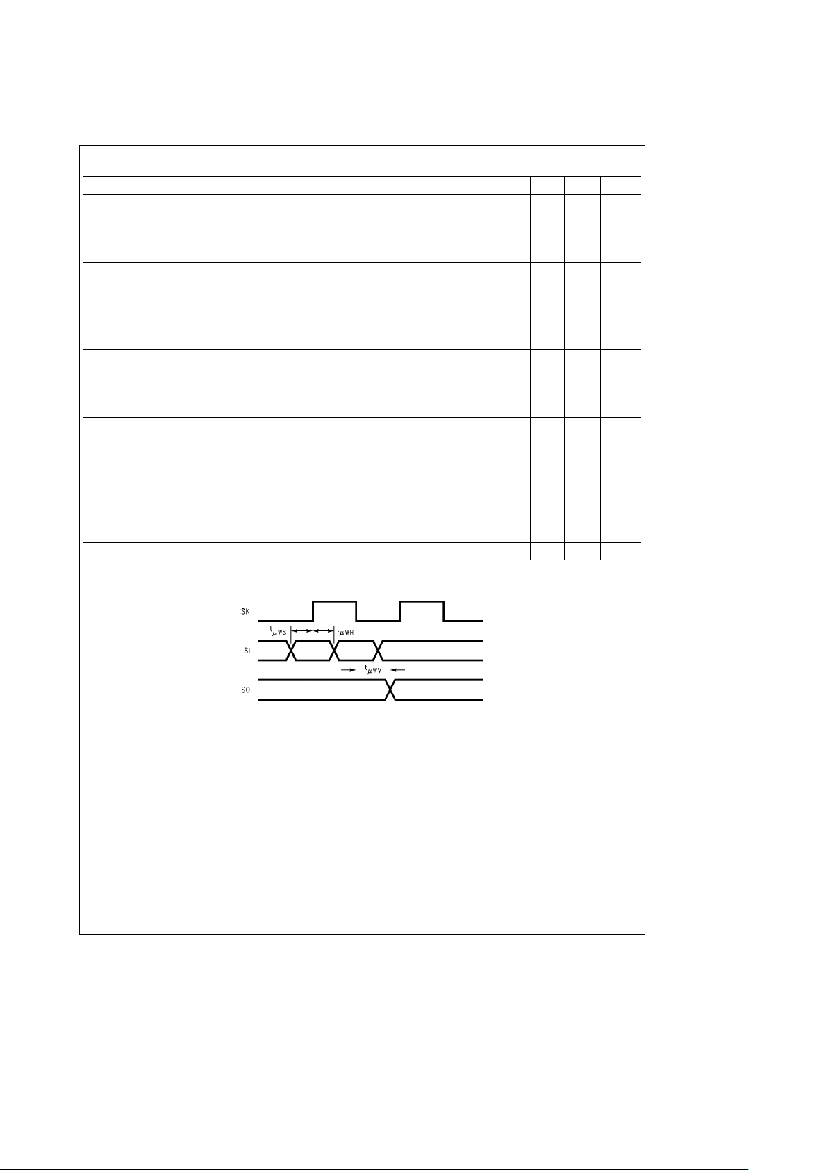
ICSS1001 AC Electrical Characteristics (
b
40§CkT
A
k
a
85§C)
Symbol Parameter Conditions Min Typ Max Units
(tc) Instruction Cycle Time
Crystal/Resonator V
CC
t
4.0V 1.0 DC
ms
2.5
s
V
CC
s
4.0V 2.5 DC
R/C Oscillator V
CC
t
4.0V 3.0 DC
2.5
s
V
CC
s
4.0V 7.5 DC
CKI Clock Duty Cycle (Note 1) feMax 40 60 %
t
SETUP
Inputs
t
HOLD
V
CC
t
4.5V 200
ns
2.5
s
V
CC
s
4.0V 500
V
CC
t
4.5V 60
2.5
s
V
CC
s
4.0V 150 ns
(t
PD1,tPD0
) Output Propagation Delay C
L
e
100 pF, R
L
e
2.2k
SK, SO V
CC
t
4.5V
ms
2.5
s
V
CC
s
4.0V 0.7
All Others V
CC
t
4.5V 1
2.5
s
V
CC
s
4.0V 2.5
(t
UWS
) MICROWlRE
(t
UWH
) Setup Time (Note 1) 20
ns
(t
UPD
) Hold Time (Note 1) 56
Output Propagation Delay 220
Input Pulse Width (Note 2)
Interrupt High Time 1
t
c
Interrupt Low Time 1
Timer 1, 2 High Time 1
Timer 1, 2 Low Time 1
Reset Pulse Width (Note 1) 1.0 ms
Note 1: Parameter characterized but not tested.
Note 2: t
c
e
Instruction Cycle Time.
TL/DD/11727– 5
10
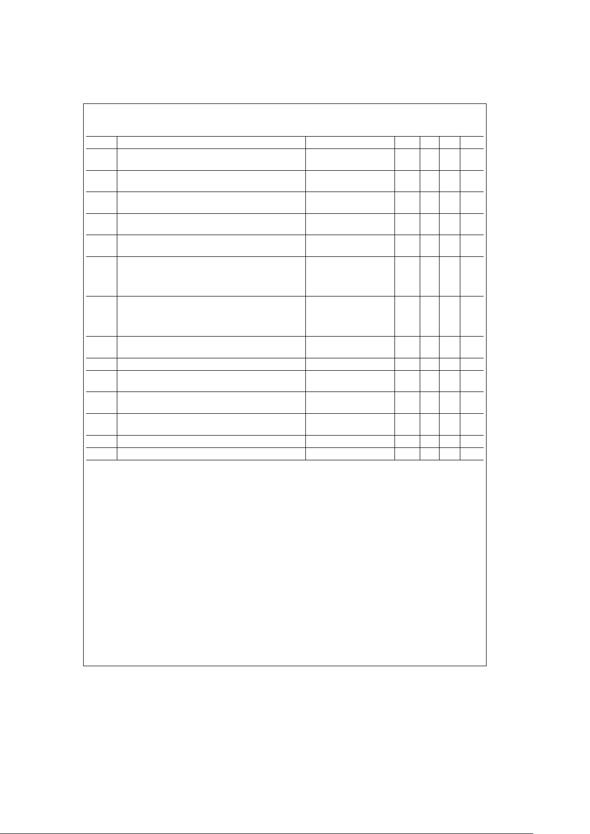
ICSS1002 DC Electrical Characteristics
Specified at V
CC
e
5Vg10%, V
SS
e
GND, over all temperature ranges unless otherwise specified.
Symbol Parameter Conditions Min Typ Max Units
V
IL
Low Level Input Voltage (Note 1) V
CC
e
4.5V
V
TTL Level 0.8
V
IH
High Level Input Voltage (Note 1) V
CC
e
5.5V
V
TTL Level 2.0
V
T
a
Positive-Going Threshold VoltageÐSchmitt Trigger (Note 1) V
CC
e
5.5V
3.9 V
V
T
b
Negative-Going Threshold VoltageÐSchmitt Trigger (Note 1) V
CC
e
5.5V
1.0 V
V
H
Hysteresis VoltageÐSchmitt Trigger (Note 1) V
CC
e
5.5V
1.0 1.6 V
I
IL
Low Level Input Leakage Current V
IN
e
GND, V
CC
e
5.5V
Without Pull-Down Resistor
b
10
mA
With Pull-Up Resistor
b
200
With Pull-Down Resistor
b
10
I
IH
High Level Input Leakage Current V
IN
e
V
CC
e
5.5V
Without Pull-Down Resistor 10
mA
With Pull-Up Resistor 10
With Pull-Down Resistor 200
V
OL
Low Level Output Voltage I
OL
e
4 mA, V
CC
e
4.5V 0.5
V
Reset I
OL
e
12 mA, V
CC
e
4.5V 0.5
V
OH
High Level Output Voltage I
OL
eb
4 mA, V
CC
e
4.5V 3.7 V
I
OZL
Low Level Output Leakage Current (Note 2) V
O
e
GND, V
CC
e
5.5V
b
160 mA
V
IN
e
V
IL
I
OZH
High Level Output Leakage Current (Note 2) V
O
e
V
CC
e
5.5V
160 mA
V
IN
e
V
IL
I
CC
Power Supply Current Drain, DC (Note 3) V
CC
e
5.5V
1mA
CINInput Capacitance (Note 1) 20 pF
C
OUT
Output Capacitance (Note 1) 20 pF
Note 1: Specification is guaranteed by design. This test cannot be performed unless a hook-up to a special output is defined.
Note 2: I
OZ
specifications are for output buffers without pull-up or pull-down resistors.
Note 3: DC means at power on with CLK and POWER ON RC inputs low, all other signal pins open.
11
 Loading...