© 2000 National Semiconductor Corporation www.national.com
Geode™ GXm Processor Integrated x86 Solution with MMX Support
April 2000
Geode™ GXm Processor
Integrated x86 Solution with MMX Support
General Description
The National Semiconductor®Geode™ GXm processor
is an advanced 32-bit x86 compatible processor offering
high performance, fully accelerated 2D graphics, a 64-bit
synchronous DRAM controller and a PCI bus controller,
all on a single chip that is compatible with Intel’s MMX
technology.
The GXm processor core is a proven design that offers
competitive CPU performance. It has integer and floating
point execution units that are based on sixth-generation
technology. The integer core contains a single, six-stage
execution pipeline and offers advanced features such as
operand forwarding, branch target buffers, and extensive
write buffering. A 16 KB write-back L1 cache is accessed
in a unique fashion that eliminates pipeline stalls to fetch
operands that hit in the cache.
In addition to the advanced CPU features, the GXm processor integrates a host of functions which are typically
implemented with external components. A full-function
graphics accelerator provides pixel processing and rendering functions.
A separate on-chip video buffer enables >30 fps MPEG1
video playback when used together with the CS5530 I/O
companion chip. Graphics and system memory accesses
are supported by a tightly-coupled synchronous DRAM
(SDRAM) memory controller.This tightly coupledmemory
subsystem eliminates the need for an external L2 cache.
The GXm processor includes Virtual System Architecture
®
(VSA™ technology) enabling XpressGRAPHICS
and XpressAUDIO subsystems as well as generic emulation capabilities. Softwarehandler routines forthe XpressGRAPHICS and XpressAUDIO subsystems can be
included in the BIOS and provide compatible VGAand 16bit industry standard audio emulation.XpressAUDIO technologyeliminatesmuch of the hardware traditionallyassociated with audio functions.
Geode™ GXm Processor Internal Block Diagram
Write-Back
Unit
FPU
Internal Bus Interface Unit
Graphics Memory Display PCI
SDRAM Port CS5530
PCI Bus
Integer
Cache Unit
Integrated
Functions
MMU
(CRT/LCD TFT)
X-Bus
Pipeline Controller Controller Controller
C-Bus
National Semiconductor and Virtual System Architecture are registered trademarks of National Semiconductor Corporation.
Geode and VSA aretrademarks of National Semiconductor Corporation.
For a complete listing of National Semiconductor trademarks, pleasevisit www.national.com/trademarks.
www.national.com 2 Revision 3.1
Geode™ GXm Processor
Features
General Features
Packaged in:
— 352-Terminal Ball Grid Array (BGA) or
— 320-Pin Staggered Pin Grid Array (SPGA)
0.35-micron fourlayer metal CMOS process
Split rail design (3.3V I/O and 2.9V core)
32-Bit x86 Processor
Supports the MMX instruction set extension for the
acceleration of multimedia applications
Speeds offered up to 266 M Hz
16 KB unified L1 cache
Integrated Floating P oint Unit (FPU)
Re-entrant System Management Mode (SMM)
enhanced for VSA
PCI Controller
Fixed, rotating, hybrid, or ping-pong arbitration
Supports up to three PCI bus masters
Synchronous CPU and PCI bus clock frequency
Supports concurrency between PCI master andL1
cache
Power Management
Designed to support CS5530 power management
architecture
CPU only Suspend or full 3V Suspend supported:
— Clocks to CPU core stopped for CPU Suspend
— All on-chip clocks stopped for 3V Suspend
— Suspend refresh supported for 3V Suspend
Virtual Systems Architecture Technology
Architecture allows OS independent (software) virtualization of hardware functions
Provides compatiblehigh performance legacy VGA
core functionality
Note: GUI (GraphicalUser Interface) graphics accel-
eration is pure hardware.
Provides 16-bit XpressAUDIO subsystem
2D Graphics Accelerator
Graphics pipeline performance significantly increased
over previous generations by pipelining burst
reads/writes
Accelerates BitBL Ts, line draw, text
Supports all 256rasteroperations
Supports transparent BLTs
Runs at core clock frequency
Full VGA and VESA mode support
Special "Driver level”instructions utilize internal
scratchpad for enhanced performance
Display Controller
Video Generator (VG) improves memory efficiency for
display refresh with SDRAM
Supports a separate MPEG1 video buffer and data
path to enable video acceleration in the CS5530
Internal palette RAM for use with the CS5530
Direct interface to CS5530 for CRT and TFT flatpanel
support which eliminates need for external RAMDAC
Hardware frame buffer compressor/decompressor
Hardware cursor
Supports up to1280x1024x8 bpp and1024x768x16
bpp
XpressRAM Subsystem
Memory control/interface directly from CPU
64-Bit wide memory bus
Support for:
— Two 168-pin unbuffered DIMMs
— Up to 16open banks simultaneously
— Single or 16-byte reads (burst length of two)

Revision 3.1 3 www.national.com
Table of Contents
Geode™ GXm Processor
1.0 ArchitectureOverview............................................. 8
1.1 INTEGERUNIT ...........................................................8
1.2 FLOATINGPOINTUNIT ....................................................9
1.3 WRITE-BACKCACHEUNIT .................................................9
1.4 MEMORYMANAGEMENTUNIT..............................................9
1.4.1 InternalBusInterfaceUnit ............................................9
1.5 INTEGRATED FUNCTIONS . . . . .............................................9
1.5.1 Graphics Accelerator . . . .............................................9
1.5.2 DisplayController..................................................10
1.5.3 XpressRAMMemorySubsystem ......................................10
1.5.4 PCIController.....................................................10
1.6 GEODEGXM/CS5530SYSTEMDESIGNS ....................................11
2.0 SignalDefinitions................................................ 13
2.1 PINASSIGNMENTS ......................................................13
2.2 SIGNALDESCRIPTIONS ..................................................24
2.2.1 SystemInterfaceSignals ............................................24
2.2.2 PCIInterfaceSignals ...............................................26
2.2.3 MemoryControllerInterfaceSignals ...................................29
2.2.4 VideoInterfaceSignals .............................................30
2.2.5 Power,Ground,andNoConnectSignals................................32
2.2.6 InternalTestandMeasurementSignals ................................32
2.3 SUBSYSTEMSIGNALCONNECTIONS .......................................34
2.4 POWERPLANES.........................................................36
3.0 ProcessorProgramming .......................................... 38
3.1 COREPROCESSORINITIALIZATION........................................38
3.2 INSTRUCTIONSETOVERVIEW.............................................39
3.2.1 LockPrefix .......................................................39
3.3 REGISTERSETS.........................................................40
3.3.1 ApplicationRegisterSet.............................................40
3.3.2 SystemRegisterSet ...............................................44
3.3.3 ModelSpecificRegisterSet..........................................59
3.3.4 TimeStampCounter ...............................................59
3.4 ADDRESSSPACES.......................................................60
3.4.1 I/OAddressSpace.................................................60
3.4.2 MemoryAddressSpace.............................................60
3.5 OFFSET,SEGMENT,ANDPAGINGMECHANISMS .............................61
3.6 OFFSETMECHANISM ....................................................61
3.7 DESCRIPTORSANDSEGMENTMECHANISMS................................62
3.7.1 Real and Virtual 8086 Mode Segment Mechanisms . . . . . . . . ...............62
3.7.2 SegmentMechanisminProtectiveMode................................63
3.7.3 GDTRandLDTRRegisters ..........................................66
3.7.4 DescriptorBitStructure .............................................67
3.7.5 GateDescriptors ..................................................69
3.8 MULTITASKINGANDTASKSTATESEGMENTS................................70
3.9 PAGINGMECHANISM.....................................................72

www.national.com 4 Revision 3.1
Table of Contents (Continued)
Geode™ GXm Processor
3.10 INTERRUPTSANDEXCEPTIONS ...........................................74
3.10.1 Interrupts ........................................................74
3.10.2 Exceptions .......................................................74
3.10.3 InterruptVectors...................................................75
3.10.4 InterruptandExceptionPriorities......................................76
3.10.5 ExceptionsinRealMode ............................................77
3.10.6 ErrorCodes ......................................................77
3.11 SYSTEMMANAGEMENTMODE ............................................78
3.11.1 SMMEnhancements ...............................................79
3.11.2 SMMOperation ...................................................79
3.11.3 TheSMI#Pin .....................................................80
3.11.4 SMMConfigurationRegisters ........................................80
3.11.5 SMMMemorySpaceHeader.........................................80
3.11.6 SMMInstructions ..................................................82
3.11.7 SMMMemorySpace ...............................................83
3.11.8 SMIGeneration ...................................................83
3.11.9 SMIServiceRoutineExecution .......................................83
3.12 SHUTDOWNANDHALT ...................................................86
3.13 PROTECTION ...........................................................86
3.13.1 PrivilegeLevels ...................................................86
3.13.2 I/OPrivilegeLevels ................................................86
3.13.3 PrivilegeLevelTransfers ............................................87
3.13.4 InitializationandTransitiontoProtectedMode............................87
3.14 VIRTUAL8086MODE .....................................................88
3.14.1 MemoryAddressing................................................88
3.14.2 Protection........................................................88
3.14.3 Interrupt Handling . . . . . . ............................................88
3.14.4 EnteringandLeavingVirtual8086Mode................................88
3.15 FLOATINGPOINTUNITOPERATIONS .......................................89
3.15.1 FPU(FloatingPointUnit)RegisterSet..................................89
3.15.2 FPUTagWordRegister .............................................89
3.15.3 FPUStatusRegister ...............................................89
3.15.4 FPUModeControlRegister ..........................................89
4.0 Integrated Functions . . . . . . . . . . . . . . . . . . . . . . . . . . . . . . . . . . . . . . . . . . . . . 91
4.1 INTEGRATED FUNCTIONS PROGRAMMING INTERFACE . . . . . . . . ...............92
4.1.1 Graphics Control Register . . . . . . . . . . . . . . . ............................92
4.1.2 ControlRegisters ..................................................94
4.1.3 Graphics Memory . . . . . . ............................................94
4.1.4 L1CacheController ................................................95
4.1.5 DisplayDriverInstructions ...........................................98
4.1.6 CPU_READ/CPU_WRITEInstructions .................................99
4.2 INTERNALBUSINTERFACEUNIT..........................................100
4.2.1 FPUErrorSupport ................................................100
4.2.2 A20MSupport ...................................................100
4.2.3 SMIGeneration ..................................................100
4.2.4 640KBto1MBRegion ............................................100
4.2.5 InternalBusInterfaceUnitRegisters ..................................101

Revision 3.1 5 www.national.com
Table of Contents (Continued)
Geode™ GXm Processor
4.3 MEMORYCONTROLLER .................................................103
4.3.1 MemoryArrayConfiguration ........................................104
4.3.2 MemoryOrganizations.............................................105
4.3.3 SDRAMCommands...............................................106
4.3.4 MemoryControllerRegisterDescription ...............................108
4.3.5 AddressTranslation ...............................................112
4.3.6 MemoryCycles ..................................................115
4.3.7 SDRAMInterfaceClocking..........................................118
4.4 GRAPHICSPIPELINE ....................................................120
4.4.1 BitBLT/VectorEngine ..............................................120
4.4.2 Master/SlaveRegisters ............................................121
4.4.3 PatternGeneration................................................121
4.4.4 SourceExpansion ................................................123
4.4.5 RasterOperations ................................................123
4.4.6 Graphics Pipeline Register Descriptions . . . . ...........................124
4.5 DISPLAYCONTROLLER..................................................129
4.5.1 DisplayFIFO ....................................................130
4.5.2 CompressionTechnology...........................................130
4.5.3 Motion Video Acceleration Support . . . . . . . . ...........................130
4.5.4 HardwareCursor .................................................131
4.5.5 DisplayTimingGenerator...........................................131
4.5.6 DitherandFrame-RateModulation ...................................131
4.5.7 DisplayModes ...................................................131
4.5.8 Graphics Memory Map . . ...........................................135
4.5.9 DisplayControllerRegisters.........................................136
4.5.10 MemoryOrganizationRegisters......................................144
4.5.11 TimingRegisters .................................................146
4.5.12 CursorPositionRegisters...........................................149
4.5.13 ColorRegisters ..................................................150
4.5.14 PaletteAccessRegisters ...........................................151
4.5.15 CS5530DisplayControllerInterface ..................................153
4.6 PCICONTROLLER ......................................................155
4.6.1 X-BusPCISlave..................................................155
4.6.2 X-BusPCIMaster ................................................155
4.6.3 PCIArbiter ......................................................155
4.6.4 GeneratingConfigurationCycles .....................................155
4.6.5 GeneratingSpecialCycles..........................................155
4.6.6 PCIConfigurationSpaceControlRegisters.............................156
4.6.7 PCIConfigurationSpaceRegisters ...................................157
4.6.8 PCICycles ......................................................162
5.0 VirtualSubsystemArchitecture ................................... 165
5.1 VIRTUALVGA ..........................................................165
5.1.1 TraditionalVGAHardware ..........................................165
5.2 GXMVIRTUALVGA......................................................167
5.2.1 DatapathElements................................................167
5.2.2 VideoRefresh ...................................................168
5.2.3 GXmVGAHardware ..............................................168
5.2.4 VGAVideoBIOS .................................................171
5.2.5 VirtualVGARegisterDescriptions ....................................172

www.national.com 6 Revision 3.1
Table of Contents (Continued)
Geode™ GXm Processor
6.0 PowerManagement ............................................. 174
6.1 APMSUPPORT .........................................................174
6.2 CPUSUSPENDCOMMANDREGISTERS ....................................174
6.3 SUSPENDMODULATION .................................................174
6.4 3-VOLTSUSPENDMODE.................................................174
6.5 SUSPENDMODEANDBUSCYCLES .......................................175
6.5.1 InitiatingSuspendwithSUSP# ......................................175
6.5.2 InitiatingSuspendwithHALT ........................................176
6.5.3 RespondingtoaPCIAccessDuringSuspendMode......................177
6.5.4 Stopping the Input Clock ...........................................178
6.6 GXM PROCESSORSERIALBUS ..........................................179
6.6.1 SerialPacketTransmission .........................................179
6.7 POWERMANAGEMENTREGISTERS .......................................179
7.0 ElectricalSpecifications.......................................... 182
7.1 PARTNUMBERS........................................................182
7.2 ELECTRICALCONNECTIONS .............................................182
7.2.1 Power/GroundConnectionsandDecoupling ............................182
7.2.2 Power Sequencing the Core and I/O Voltages ...........................182
7.2.3 NC-DesignatedPins...............................................182
7.2.4 Pull-UpandPull-DownResistors .....................................182
7.2.5 UnusedInputPins ................................................182
7.3 ABSOLUTEMAXIMUMRATINGS...........................................183
7.4 OPERATINGCONDITIONS................................................184
7.5 DCCHARACTERISTICS ..................................................185
7.6 ACCHARACTERISTICS ..................................................186
8.0 PackageSpecifications .......................................... 195
8.1 THERMALCHARACTERISTICS ............................................195
8.1.1 HeatsinkConsiderations ...........................................196
8.2 MECHANICALPACKAGEOUTLINES........................................198
9.0 InstructionSet.................................................. 201
9.1 GENERALINSTRUCTIONSETFORMAT.....................................202
9.1.1 Prefix(Optional) .................................................203
9.1.2 Opcode.........................................................203
9.1.3 modandr/mByte(MemoryAddressing) ...............................205
9.1.4 regField ........................................................206
9.1.5 s-i-bByte(Scale,Indexing,Base) ....................................207
9.2 CPUIDINSTRUCTION....................................................208
9.2.1 Standard CPUID Levels . ...........................................208
9.2.2 ExtendedCPUIDLevels............................................210
9.3 PROCESSORCOREINSTRUCTIONSET ....................................212
9.4 FPUINSTRUCTIONSET..................................................224
9.5 MMXINSTRUCTIONSET .................................................229
9.6 NATIONAL S EMICONDUCTOR EXTENDED MMX INSTRUCTION SET . . . . . . . . . . . . . 234

Revision 3.1 7 www.national.com
Table of Contents (Continued)
Geode™ GXm Processor
Appendix A Support Documentation . . . . . . . . . . . . . . . . . . . . . . . . . . . . . . . . . . . . . 236
A.1 ORDERINFORMATION ..................................................236
A.2 DATABOOKREVISIONHISTORY ..........................................236
www.national.com 8 Revision 3.1
Geode™ GXm Processor
1.0 Architecture Overview
The National Semiconductor Geode GXm processor is
an x86-compatible 32-bit microprocessor. The decoupled
load/store unit (within the memory management unit)
allows multiple instructions in a single clock cycle. Other
features include single-cycle execution, single-cycle
instruction decode, 16 KB write-back cache, and clock
ratesupto266MHz.Thesefeaturesaremadepossible
by the use of advanced-process technologies and superpipelining.
The GXm processor has low power consumption at all
clock frequencies. Where additional power savings are
required, designerscanmake use of Suspend mode,Stop
Clock capability, and System Management Mode (SMM).
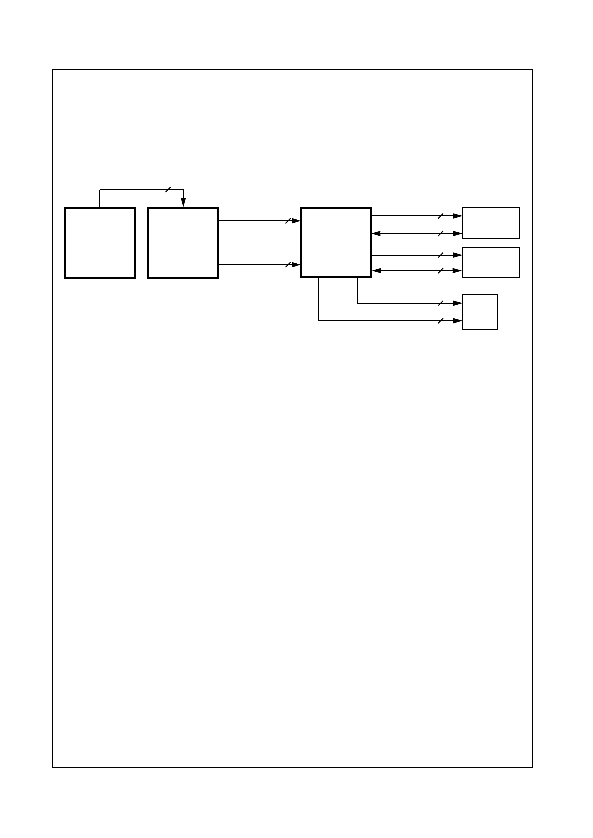
The GXm processor is divided into major functional blocks
(as shown in Figure 1-1):
• Integer Unit
• Floating Point Unit (FPU)
• Write-Back Cache Unit
• Memory Management Unit (MMU)
• Internal Bus Interface Unit
• IntegratedFunctions
Instructions are executed in the integer unit and in the
floating point unit. The cache unit stores the most recently
used data and instructions and provides fast access to
this information for the integer and floating point units.
1.1 INTEGER UNIT
The integer unit consists of:
• Instruction Buffer
• Instruction Fetch
• Instruction Decoder and Execution
The superpipelined integer unit fetches, decodes, and
executes x86 instructions through the use of a six-stage
integer pipeline.
The instruction fetch pipeline stage generates, from the
on-chip cache, a continuous high-speed instruction
stream for use by the processor. Up to 128 bits of code
are read during a single clock cycle.
Branch prediction logic within the prefetch unit generates
a predicted target address for unconditional or conditional
branch instructions. When a branch instruction is
detected, the instruction fetchstage starts loading instructions at the predicted address within a single clock cycle.
Up to 48 bytes of code are queued prior to the instruction
decode stage.
The instruction decode stage evaluates the code stream
provided bythe instructionfetchstageanddeterminesthe
number of bytes in each instruction and the instruction
type. Instructions are processed and decoded at a maximum rate of one instruction per clock.
The address calculation function is super-pipelined and
contains two stages, AC1 and AC2. If the instruction
refers to a memory operand, AC1 calculates a linear
memory address for the instruction.
The AC2 stage performs any required memory management functions, cache accesses, and register file
accesses. If a floating point instruction is detected by
AC2, the instruction is sent to the floating point unit for
processing.
The execution stage, under control of microcode, executes instructions using the operands provided by the
address calculation stage.
Write-back, the last stage of the integer unit, updates the
register file within the integer unit or writes to the
load/store unit within the memory managementunit.
Figure 1-1. Internal Block Diagram
Write-Back
Unit
FPU
Internal Bus Interface Unit
Graphics Memory Display PCI
SDRAM Port CS5530
PCI Bus
Integer
Cache Unit
Integrated
Functions
MMU
(CRT/LCD TFT)
X-Bus
Pipeline Controller Controller Controller
C-Bus

Revision 3.1 9 www.national.com
Architecture Overview (Continued)
Geode™ GXm Processor
1.2 FLOATING POINT UNIT
The FPU (Floating PointUnit)interfaces to the integer unit
and the cache unit through a 64-bit bus. The FPU is x87instruction-set compatible and adheres to the IEEE-754
standard. Because almost all applications that contain
FPU instructions also contain integer instructions, the
GXm processor’s FPU achieves high performance by
completing integer and FPU operations in parallel.
FPU instructions are dispatched to the pipeline within the
integer unit. The address calculation stage of the pipeline
checks for memory management exceptions and
accesses memory operandsforusebytheFPU. Once the
instructionsandoperands havebeenprovided to the FPU,
the FPU completes instruction execution independently of
the integer unit.
1.3 WRITE-BACK CACHE UNIT
The 16 KB write-back unified cache is a data/instruction
cache and is configured as four-way set associative. The
cache stores up to 16 KB of code and data in 1024 cache
lines.
The GXm processor provides the ability to allocate a portion of the L1 cache as a scratchpad, which is used to
accelerate the Virtual Systems Architecture algorithms as
well as for some graphics operations.
1.4 MEMORY MANAGEMENT UNIT
The memory management unit (MMU) translates the linear address supplied by the integer unit into a physical
address to be used by the cache unit and the internal bus
interface unit. Memory management procedures are x86compatible, adhering to standard paging mechanisms.
The MMU also contains a load/store unit that is responsible for scheduling cache and external memory accesses.
The load/store unit incorporates two performanceenhancing features:
• Load-store reordering that gives priority to memory
reads required by the integer unit over writes to
external memory.
• Memory-read bypassing that eliminates unnecessary
memory reads by using valid data from the execution
unit.
1.4.1 Internal Bus Interface Unit
The internal bus interface unit provides a bridge from the
GXm processor to the integrated system functions (i.e.,
memory subsystem, display controller, graphics pipeline)
and the PCI bus interface.
When external memory access is required, the physical
address is calculated by the memory management unit
and then passed to the internal bus interface unit, which
translates the cycle to an X-Bus cycle (the X-Bus is a
National Semiconductor proprietary internal bus which
provides a common interface for all of the system modules). The X-Bus memory cyclenow is arbitrated between
other pending X-Bus memory requests to the SDRAM
controller before completing.
In addition, the internal bus interface unit provides configuration control for up to 20 different regions within system
memory with separate controls for read access, write
access, cacheability, and PCI access.
1.5 INTEGRATED FUNCTIONS
The GXm processor integrates the following functions traditionally implemented using external devices:
• High-performance2D graphicsaccelerator
• Separate CRT and TFT data paths from the display
controller
• SDRAM memory controller
• PCI bridge
The processor has also been enhanced to support
National Semiconductor’s proprietary Vir tual System
Architecture (VSA) implementation.
The GXm processor implements a Unified Memory Architecture (UMA). By using National Semiconductor’s Display Compression Technology (DCT), the performance
degradation inherent in traditional UMA systems is eliminated.
1.5.1 Graphics Accelerator
The graphics accelerator is a full-featured GUI (Graphical
User Interface) accelerator. The graphics pipeline implements a bitBLT engine for frame buffer bitBLTs and rectangular fills. Additional instructions in the integer unit may
be processed, as the bitBLT engine assists the CPU in the
bitBLT operations that take place between system memory and the frame buffer. This combination of hardware
and software is used by the display dr iver to provide very
fast transfers in both directions between system memory
and the frame buffer. The bitBLT engine also draws randomly-oriented vectors, and scanlines for polygon fill. All
of the pipeline operations described in the following list
can be applied to anybitBLT operation.
• Pattern Memory.Render with 8x8 dither, 8x8 monochrome, or 8x1 color pattern.
• Color Expansion. Expand monochrome bitmaps to
full-depth 8- or 16-bit colors.
• Transparency. Suppresses drawing of background
pixels for transparenttext.
• Raster Operations. Boolean operation combines
source, destination, and pattern bitmaps.

www.national.com 10 Revision 3.1
Architecture Overview (Continued)
Geode™ GXm Processor
1.5.2 Display Controller
The display port is a direct interface to the CS5530 which
drives a TFT flat panel display, LCD panel, or a CRT display.
The display controller (video generator) retrieves image
data from the frame buffer region of memory, performs a
color-look-up if required, inserts the cursor overlay into
the pixel stream, generates display timing, and formats
the pixel data for output to a variety of display devices.
The display controller contains Display Compression
Technology (DCT) that allows the GXm processor to
refresh the display from a compressed copy of the frame
buffer. DCT typically decreases the screen-refresh bandwidth requirement by a factor of 15 to 20, further minimizing bandwidth contention.
1.5.3 XpressRAM Memory Subsystem
The memory controller drives a 64-bit SDRAM port
directly. The SDRAM memory array contains both the
main system memory and the graphicsframebuffer. Up to
four module banks of SDRAM are supported. Each module bank will have two or four component banks depending on the memory size and organization. The maximum
configuration is four module banks with four component
banks providing a total of 16 open banks. The maximum
memory size is 1 GB.
The memory controller handles multiple requests for
memory data from the GXm processor, the graphics
accelerator and the display controller. The memory controller contains extensive buffering logic that helps minimize contention for memory bandwidth between graphics
and CPU requests. The memory controller cooperates
with the internal bus controller to determine the cacheability of all memory references.
1.5.4 PCI Controller
The GXm processor incorporates a full-function PCI interface module that includes the PCI arbiter. All accesses to
external I/O devices are sent over the PCI bus, although
most memory accesses are serviced by the SDRAM controller. The Internal Bus Interface Unit contains address
mapping logic that determines if memory accesses are
targeted for the SDRAM or for the PCI bus.
Revision 3.1 11 www.national.com
Architecture Overview (Continued)
Geode™ GXm Processor
1.6 GEODE GXM/CS5530 SYSTEM DESIGNS
The GXm Integrated Subsystem with MMX support consists of two chips, the GXm Processor and the CS5530
I/O companion. The subsystem provides high performance using 32-bit x86 processing. The two chips integrate video, audio and memory interface functions
normally performed by external hardware.
As described in separate manuals, the CS5530 enables
the full features of the GXm processor with MMX support.
These features include full VGA and VESA video, 16-bit
stereo sound, IDE interface, ISA interface, SMM power
management, and AT compatibility logic. In addition, the
newer CS5530 provides an Ultra DMA/33 interface,
MPEG2 assist, and AC97 Version 2.0 compliant audio.
Figure 1-2 shows a basic block system diagram (refer to
Figure 2-4 on page 34 for detailed subsystem interconnection signals). It includes the National Semiconductor
CS9210 Dual-Scan Flat Panel Display Controller for
designs that need to interfaceto a DSTN panel (instead of
TFT panel).
Figure 1-2. Geode™ GXm/CS5530 System Block Diagram
YUV Port
(Video)
RGB Port
PCI Interface
SDRAM
MD[63:0]
PCI Bus
Geode™ CS5530
I/O Companion
Graphics Data
Video Data
Analog RGB
Digital RGB (to TFT or DSTN Panel)
CRT
TFT
Panel
USB
(2 Ports)
AC97
Codec
Speakers
CD
ROM
Audio
Microphone
GPIO
Port
(Graphics)
Super
ISA Bus
SDRAM
Serial
Packet
Clocks
I/O
BIOS
IDE
Devices
14.31818
MHz Crystal
IDE Control
System
Clocks
DC-DC & Battery
CS9210
DSTN
Controller
DSTN Panel
Geode™ GXm
Processor
Geode™
www.national.com 12 Revision 3.1
Architecture Overview (Continued)
Geode™ GXm Processor
The CS9210 converts the digital RGB output of the
CS5530 I/O companion chip to the digital output suitable
for driving a dual-scan color STN (DSTN) flat panel LCD.
It connects to the digital RGB output of a GXm processor
or 55x0 and drives the graphics data onto a dual-scan flat
panel LCD. It can drive all standard dual-scan color STN
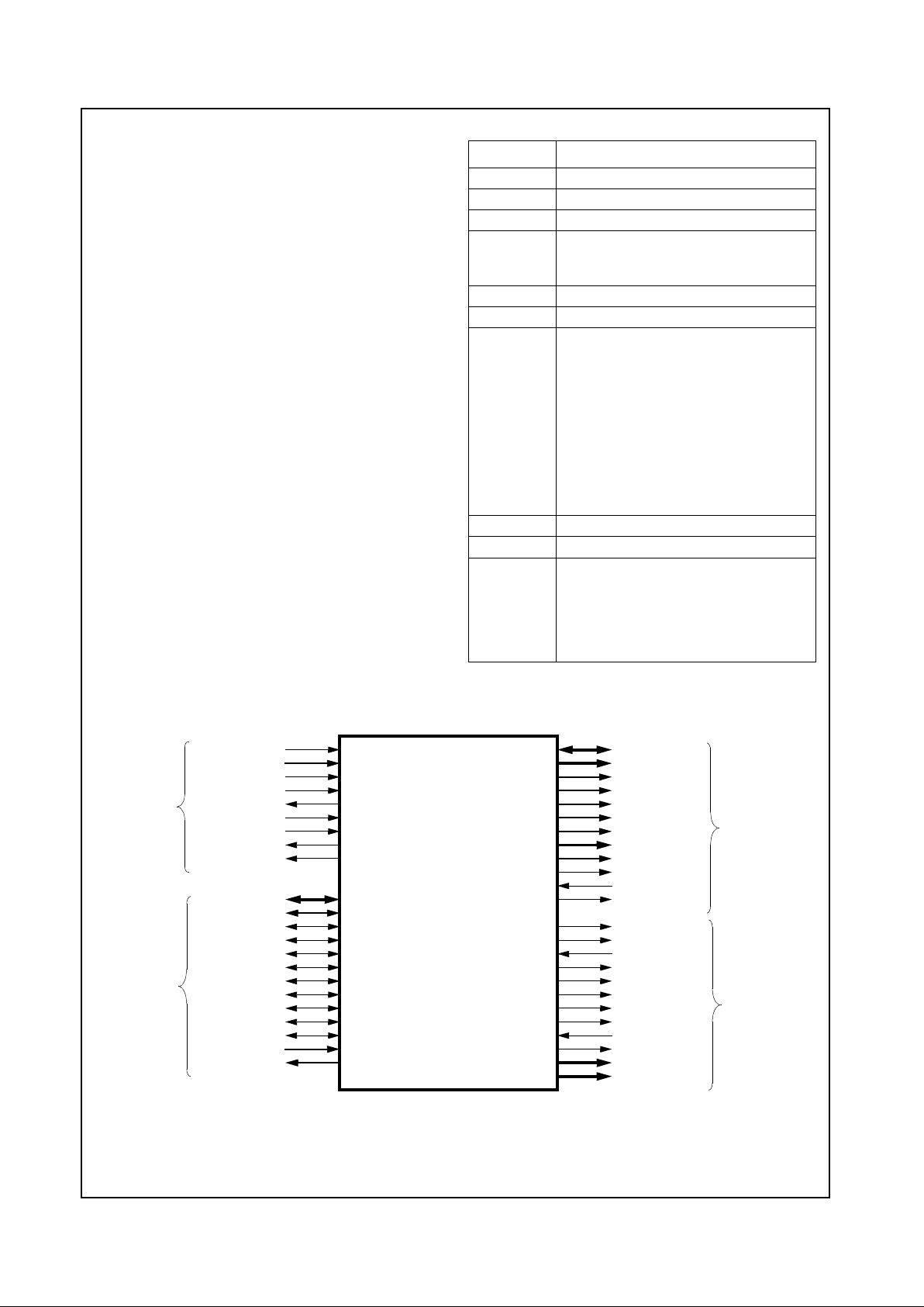
flat panels up to 1024x768 resolution. Figure 1-3 shows
an example of a CS9210 interface in a typical GXm Integrated Subsystem.
Figure 1-3. CS9210 Interface System Diagram
DRAM Data
Address Control
13
16
Panel Control
6
24
Panel Data
DSTN
Pixel Port
24
Pixel Data
LCD
18
CS5530
CS9210
DSTN
Controller
I/O
DRAM-B
256Kx16 Bit
DRAM-A
256Kx16 Bit
Address Control
13
DRAM Data
16
4
Serial
Configuration
Companion
(Control & Data)
Geode™ GXm
Processor
Geode™
Geode™
Revision 3.1 13 www.national.com
Geode™ GXm Processor
2.0 Signal Definitions
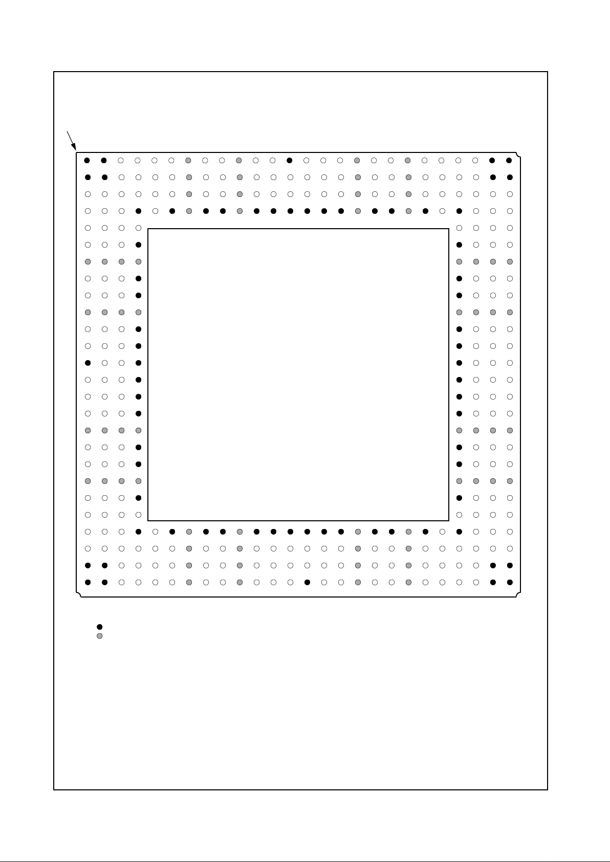
This section describes the external interface of the Geode
GXm processor. Figure 2-1 shows the signals organized
by their functional interface groups (internal test and electrical pins are not shown).
2.1 PIN ASSIGNMENTS
The tables in this section use several common abbreviations. Table 2-1 lists the mnemonics and their meanings.
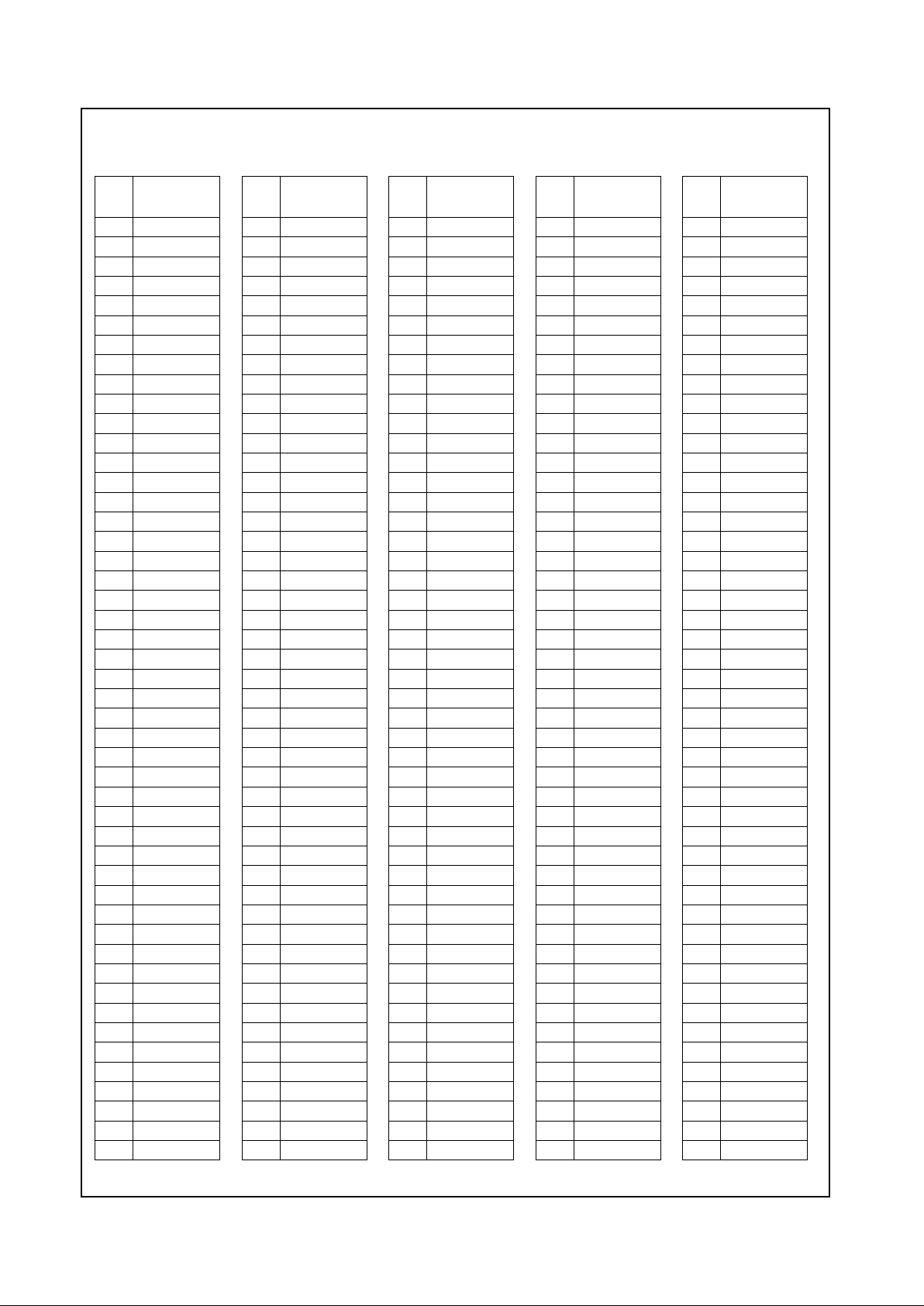
Figure 2-2 on page 14 shows the pin assignment for the
352 BGA with Tables 2-2 and 2-3 listing the pin assignments sorted by pin number and alphabetically by signal
name, respectively.
Figure 2-3 on page 19 shows the pin assignment for the
320 SPGA with Tables 2-4 and 2-5 listing the pin assignments sorted by pin number and alphabetically by signal
name, respectively.
In Section 2.2 “Signal Descriptions” starting on Page24 a
description of each signal is provided within its associated
functional group.
Following the signal descriptions, information regarding
subsystem signal connections and split power planes and
decoupling is provided.
.
Figure 2-1. Functional Block Diagram
Table 2-1. Pin Type Definitions
Mnemonic Definition
I Standardinput pin.
I/O Bidirectional pin.
O Totem-pole output.
OD Open-drain output structure that allows
multiple devicesto share the pin in a
wired-OR configuration
PU Pull-up resistor
PD Pull-down resistor
s/t/s Sustained tri-state, an active-low tri-state
signal ownedand drivenbyoneand only
one agent at a time.The agent that
drives an s/t/s pin low must drive it high
foratleast one clockbefore lettingitfloat.
A new agent cannot start driving an s/t/s
signal any sooner than one clock after
the previous owner lets it float. A pull-up
resistor is required to sustain the inactive
state until another agent drives it, and
must be provided by the central resource.
VCC (PWR) Power pin.
VSS (GND) Ground pin
# The "#" symbol at theend of a signal
name indicates that the active, or
asserted state occurs when the signal is
at a low voltage level. When "#" is not
present after the signal name, the s ignal
is asserted when at a high voltage level.
SYSCLK
CLKMODE[2:0]
RESET
INTR
IRQ13
SMI#
SUSP#
SUSPA#
SERIALP
AD[31:0]
C/BE[3:0]#
PAR
FRAME#
IRDY#
TRDY#
STOP#
LOCK#
DEVSEL#
PERR#
SERR#
REQ[2:0]#
GNT[2:0]#
MD[63:0]
MA[12:0]
BA[1:0]
RASA#, RASB#
CASA#, CASB#
CS[3:0]#
WEA#, WEB#
DQM[7:0]
CKEA, CKEB
SDCLK[3:0]
SDCLK_IN
SDCLK_OUT
PCLK
VID_CLK
DCLK
CRT_HSYNC
CRT_VSYNC
FP_VSYNC
FP_HSYNC
ENA_DISP
VID_RDY
VID_VAL
VID_DATA[7:0]
PIXEL[17:0]
Memory
Controller
Interface
Video
Interface
Signals
PCI
Interface
Signals
System
Interface
Signals
Signals
Geode™ GXm
Processor
www.national.com 14 Revision 3.1
Signal Definitions (Continued)
Geode™ GXm Processor
Figure 2-2. 35 2 BGA Pin Assignment Diagram
For order information refer to Section A.1 “Order Information” on page236.
1234567891011121314151617181920
21 22 23 24 25 26
A
B
C
D
E
F
G
H
J
K
L
M
N
P
R
T
U
V
W
Y
AA
AB
AC
AD
AE
AF
Index Corner
VSS VSS AD27 AD24 AD21 AD16 VCC2 FRAM#DEVS# VCC3 PERR# AD15 VSS AD11 CBE0# AD6 VCC2 AD4 AD2 VCC3 AD0 AD1 TEST2 MD2 VSS VSS
VSS VSS AD28 AD25 AD22 AD18 VCC2 CBE2#TRDY# VCC3 LOCK# PAR AD14 AD12 AD9 AD7 VCC2 INTR AD3 VCC3 TEST1 TEST3 MD1 MD33 VSS VSS
AD29 AD31 AD30 AD26 AD23 AD19 VCC2 AD17 IRDY# VCC3 STOP#SERR#CBE1# AD13 AD10 AD8 VCC2 AD5 SMI# VCC3 TEST0 IRQ13 MD32 MD34 MD3 MD35
GNT0# TDI REQ2# VSS CBE3# VSS VCC2 VSS VSS VCC3 VSS VSS VSS VSS VSS VSS VCC2 VSS VSS VCC3 VSS MD0 VSS MD4 MD36 TDN
GNT2#SUSPA#REQ0# AD20 MD6 TDP MD5 MD37
TD0 GNT1# TEST VSS VSS MD38 MD7 M D 39
VCC3 VCC3 VCC3 VCC3 VCC3 VCC3 VCC3 VCC3
TMS SUSP#REQ1# VSS VSS MD8 MD40 MD9
FPVSY TCLK RESET VSS VSS MD41 MD10 MD42
VCC2 VCC2 VCC2 VCC2 VCC2 VCC2 VCC2 VCC2
CKM1 FPHSYSERLP VSS VSS MD11 MD43 MD12
CKM2 VIDVALCKM0 VSS VSS MD44 MD13 MD45
VSS PIX1 PIX0 VSS VSS MD14 MD46 MD15
VIDCLK PIX3 PIX2 VSS VSS MD47 CASA#SYSCLK
PIX4 PIX5 PIX6 VSS VSS WEB# W EA# CASB#
PIX7 PIX8 PIX9 VSS VSS DQM0 DQM4 DQM1
VCC3 VCC3 VCC3 VCC3 VCC3 VCC3 VCC3 VCC3
PIX10 PIX11 PIX12 VSS VSS DQM5 CS2# CS0#
PIX13 CRTHS PIX14 VSS VSS RASA#RASB# MA0
VCC2 VCC2 VCC2 VCC2 VCC2 VCC2 VCC2 VCC2
PIX15 PIX16 CRTVS VSS VSS MA1 MA2 MA3
DCLK PIX17 VDAT6 VDAT7 MA4 MA5 MA6 MA7
PCLK FLT# VDAT4 VSS VOLDET VSS VCC2 VSS VSS VCC3 VSS VSS VSS VSS VSS VSS VCC2 VSS VSS VCC3 VSS DQM6 VSS MA8 MA9 MA10
VRDY VDAT5 VDAT3 VDAT0 EDISP MD63 VCC2 MD62 MD 29 VCC3 MD59 M D26 MD56 MD55 MD22 CKEB VCC2 MD51 MD18 VCC3 MD48 DQM3 CS1# MA11 BA0 BA1
VSS VSS VDAT2SCLK3 SCLK1RWCLK V CC2 SCKIN MD61 VCC3 MD28 MD58 MD25 MD24 MD 54 MD21 VCC2 M D 20 MD50 VCC3 M D 17 DQM7 CS3# MA12 VSS VSS
VSS VSS VDAT1SCLK0 SCLK2 MD31 V CC2SCKOUTMD30 VCC3 MD60 MD27 MD57 VSS MD23 MD53 VCC2 MD52 MD19 VCC3 MD49 MD16 DQM2 CKEA VSS VSS
1234567891011121314151617181920
21 22 23 24 25 26
A
B
C
D
E
F
G
H
J
K
L
M
N
P
R
T
U
V
W
Y
AA
AB
AC
AD
AE
AF
Geode™ GXm
352 BGA - Top View
Note: Signal names have been abbreviated in this figure due to space constraints.
= GND terminal
= PWR terminal (VCC2 = VCC_CORE; VCC3 = VCC_IO)
Processor
Revision 3.1 15 www.national.com
Signal Definitions (Continued)
Geode™ GXm Processor
Table 2-2. 352 BGA Pin Assignments - Sorted by Pin Number
Pin
No. SignalNam e
A1 VSS
A2 VSS
A3 AD27
A4 AD24
A5 AD21
A6 AD16
A7 VCC2
A8 FRAME#
A9 DEVSEL#
A10 VCC3
A11 PERR#
A12 AD15
A13 VSS
A14 AD11
A15 C/BE0#
A16 AD6
A17 VCC2
A18 AD4
A19 AD2
A20 VCC3
A21 AD0
A22 AD1
A23 TEST2
A24 MD2
A25 VSS
A26 VSS
B1 VSS
B2 VSS
B3 AD28
B4 AD25
B5 AD22
B6 AD18
B7 VCC2
B8 C/BE2#
B9 TRD Y#
B10 VCC3
B11 LOCK#
B12 PAR
B13 AD14
B14 AD12
B15 AD9
B16 AD7
B17 VCC2
B18 INTR
B19 AD3
B20 VCC3
B21 TEST1
B22 TEST3
B23 MD1
B24 MD33
B25 VSS
B26 VSS
C1 AD29
C2 AD31
C3 AD30
C4 AD26
C5 AD23
C6 AD19
C7 VCC2
C8 AD17
C9 IRDY#
C10 VCC3
C11 STOP#
C12 SERR#
C13 C/BE1#
C14 AD13
C15 AD10
C16 AD8
C17 VCC2
C18 AD5
C19 SMI#
C20 VCC3
C21 TEST0
C22 IRQ13
C23 MD32
C24 MD34
C25 MD3
C26 MD35
D1 GNT0#
D2 TDI
D3 REQ2#
D4 VSS
D5 C/BE3#
D6 VSS
D7 VCC2
D8 VSS
D9 VSS
D10 VCC3
D11 VSS
D12 VSS
D13 VSS
D14 VSS
D15 VSS
D16 VSS
D17 VCC2
D18 VSS
Pin
No. SignalName
D19 VSS
D20 VCC3
D21 VSS
D22 MD0
D23 VSS
D24 MD4
D25 MD36
D26 TDN
E1 GNT2#
E2 SUSPA#
E3 REQ0#
E4 AD20
E23 MD6
E24 TDP
E25 MD5
E26 MD37
F1 TDO
F2 GNT1#
F3 TEST
F4 VSS
F23 VSS
F24 MD38
F25 MD7
F26 MD39
G1 VCC3
G2 VCC3
G3 VCC3
G4 VCC3
G23 VCC3
G24 VCC3
G25 VCC3
G26 VCC3
H1 TMS
H2 SUSP#
H3 REQ1#
H4 VSS
H23 VSS
H24 MD8
H25 MD40
H26 MD9
J1 FP_VSYNC
J2 TCLK
J3 RESET
J4 VSS
J23 VSS
J24 MD41
J25 MD10
J26 MD42
Pin
No. SignalName
K1 VCC2
K2 VCC2
K3 VCC2
K4 VCC2
K23 VCC2
K24 VCC2
K25 VCC2
K26 VCC2
L1 CLKMODE1
L2 FP_HSYNC
L3 SERIALP
L4 VSS
L23 VSS
L24 MD11
L25 MD43
L26 MD12
M1 CLKMODE2
M2 VID_VAL
M3 CLKMODE0
M4 VSS
M23 VSS
M24 MD44
M25 MD13
M26 MD45
N1 VSS
N2 PIXEL1
N3 PIXEL0
N4 VSS
N23 VSS
N24 MD14
N25 MD46
N26 MD15
P1 VID_CLK
P2 PIXEL3
P3 PIXEL2
P4 VSS
P23 VSS
P24 MD47
P25 CASA#
P26 SYSCLK
R1 PIXEL4
R2 PIXEL5
R3 PIXEL6
R4 VSS
R23 VSS
R24 WEB#
R25 WEA#
R26 CASB#
Pin
No. SignalN ame
T1 PIXEL7
T2 PIXEL8
T3 PIXEL9
T4 VSS
T23 VSS
T24 DQM0
T25 DQM4
T26 DQM1
U1 VCC3
U2 VCC3
U3 VCC3
U4 VCC3
U23 VCC3
U24 VCC3
U25 VCC3
U26 VCC3
V1 PIXEL10
V2 PIXEL11
V3 PIXEL12
V4 VSS
V23 VSS
V24 DQM5
V25 CS2#
V26 CS0#
W1 PIXEL13
W2 CRT_HSYNC
W3 PIXEL14
W4 VSS
W23 VSS
W24 RASA#
W25 RASB#
W26 MA0
Y1 VCC2
Y2 VCC2
Y3 VCC2
Y4 VCC2
Y23 VCC2
Y24 VCC2
Y25 VCC2
Y26 VCC2
AA1 PIXEL15
AA2 PIXEL16
AA3 CRT_VSYNC
AA4 VSS
AA23 VSS
AA24 MA1
AA25 MA2
AA26 MA3
Pin
No. SignalN ame
www.national.com 16 Revision 3.1
Signal Definitions (Continued)
Geode™ GXm Processor
AB1 DCLK
AB2 PIXEL17
AB3 VID_DATA6
AB4 VID_DATA7
AB23 MA4
AB24 MA5
AB25 MA6
AB26 MA7
AC1 PCLK
AC2 FLT#
AC3 VID_DATA4
AC4 VSS
AC5 VOLDET
AC6 VSS
AC7 VCC2
AC8 VSS
AC9 VSS
AC10 VCC3
AC11 VSS
AC12 VSS
AC13 VSS
AC14 VSS
AC15 VSS
Pin
No. SignalNam e
AC16 VSS
AC17 VCC2
AC18 VSS
AC19 VSS
AC20 VCC3
AC21 VSS
AC22 DQM6
AC23 VSS
AC24 MA8
AC25 MA9
AC26 MA10
AD1 VID_RDY
AD2 VID_DATA5
AD3 VID_DATA3
AD4 VID_DATA0
AD5 ENA_DISP
AD6 MD63
AD7 VCC2
AD8 MD62
AD9 MD29
AD10 VCC3
AD11 MD59
AD12 MD26
Pin
No. SignalName
AD13 MD56
AD14 MD55
AD15 MD22
AD16 CKEB
AD17 VCC2
AD18 MD51
AD19 MD18
AD20 VCC3
AD21 MD48
AD22 DQM3
AD23 CS1#
AD24 MA11
AD25 BA0
AD26 BA1
AE1 VSS
AE2 VSS
AE3 VID_DATA2
AE4 SDCLK 3
AE5 SDCLK 1
AE6 RW_CLK
AE7 VCC2
AE8 SDCLK _IN
AE9 MD61
Pin
No. SignalName
AE10 VCC3
AE11 MD28
AE12 MD58
AE13 MD25
AE14 MD24
AE15 MD54
AE16 MD21
AE17 VCC2
AE18 MD20
AE19 MD50
AE20 VCC3
AE21 MD17
AE22 DQM7
AE23 CS3#
AE24 MA12
AE25 VSS
AE26 VSS
AF1 VSS
AF2 VSS
AF3 VID_DATA1
AF4 SDCLK0
AF5 SDCLK2
AF6 MD31
Pin
No. SignalN ame
AF7 VCC2
AF8 SDCLK_OUT
AF9 MD30
AF10 VCC3
AF11 MD60
AF12 MD27
AF13 MD57
AF14 VSS
AF15 MD23
AF16 MD53
AF17 VCC2
AF18 MD52
AF19 MD19
AF20 VCC3
AF21 MD49
AF22 MD16
AF23 DQM2
AF24 CKEA
AF25 VSS
AF26 VSS
Pin
No. SignalN ame
Table 2-2. 352 BGA Pin Assignments - Sorted by Pin Number (Continued)
Revision 3.1 17 www.national.com
Signal Definitions (Continued)
Geode™ GXm Processor
Table 2-3. 352 BGA Pin Assignments - Sorted Alphabetically by Signal Name
Signal Name Type Pin No.
AD0 I/O A21
AD1 I/O A22
AD2 I/O A19
AD3 I/O B19
AD4 I/O A18
AD5 I/O C18
AD6 I/O A16
AD7 I/O B16
AD8 I/O C16
AD9 I/O B15
AD10 I/O C15
AD11 I/O A14
AD12 I/O B14
AD13 I/O C14
AD14 I/O B13
AD15 I/O A12
AD16 I/O A6
AD17 I/O C8
AD18 I/O B6
AD19 I/O C6
AD20 I/O E4
AD21 I/O A5
AD22 I/O B5
AD23 I/O C5
AD24 I/O A4
AD25 I/O B4
AD26 I/O C4
AD27 I/O A3
AD28 I/O B3
AD29 I/O C1
AD30 I/O C3
AD31 I/O C2
BA0 O AD25
BA1 O AD26
CASA# O P25
CASB# O R26
C/BE0# I/O A15
C/BE1# I/O C13
C/BE2# I/O B8
C/BE3# I/O D5
CKEA O AF24
CKEB O AD16
CLKMODE0 I M3
CLKMODE1 I L1
CLKMODE2 I M1
CRT_HSYNC O W2
CRT_VSYNC O AA3
CS0# O V26
CS1# O AD23
CS2# O V25
CS3# O AE23
DCLK I AB1
DEVSEL# s/t/s A9 (PU)
DQM0 O T24
DQM1 O T26
DQM2 O AF23
DQM3 O AD22
DQM4 O T25
DQM5 O V24
DQM6 O AC22
DQM7 O AE22
ENA_DISP O AD5
FLT# I AC2
FP_HSYNC O L2
FP_VSYNC O J1
FRAME# s/t/s A8 (PU)
GNT0# O D1
GNT1# O F2
GNT2# O E1
INTR I B18
IRDY# s/t/s C9 (PU)
IRQ13 O C22
LOCK# s/t/s B11 (PU)
MA0 O W26
MA1 O AA24
MA2 O AA25
MA3 O AA26
MA4 O AB23
MA5 O AB24
MA6 O AB25
MA7 O AB26
MA8 O AC24
MA9 O AC25
MA10 O AC26
MA11 O AD24
MA12 O AE24
MD0 I/O D22
MD1 I/O B23
MD2 I/O A24
MD3 I/O C25
MD4 I/O D24
MD5 I/O E25
MD6 I/O E23
MD7 I/O F25
MD8 I/O H24
MD9 I/O H26
MD10 I/O J25
MD11 I/O L24
MD12 I/O L26
MD13 I/O M25
MD14 I/O N24
MD15 I/O N26
MD16 I/O AF22
MD17 I/O AE21
MD18 I/O AD19
MD19 I/O AF19
Signal Name Type PinNo.
MD20 I/O AE18
MD21 I/O AE16
MD22 I/O AD15
MD23 I/O AF15
MD24 I/O AE14
MD25 I/O AE13
MD26 I/O AD12
MD27 I/O AF12
MD28 I/O AE11
MD29 I/O AD9
MD30 I/O AF9
MD31 I/O AF6
MD32 I/O C23
MD33 I/O B24
MD34 I/O C24
MD35 I/O C26
MD36 I/O D25
MD37 I/O E26
MD38 I/O F24
MD39 I/O F26
MD40 I/O H25
MD41 I/O J24
MD42 I/O J26
MD43 I/O L25
MD44 I/O M24
MD45 I/O M26
MD46 I/O N25
MD47 I/O P24
MD48 I/O AD21
MD49 I/O AF21
MD50 I/O AE19
MD51 I/O AD18
MD52 I/O AF18
MD53 I/O AF16
MD54 I/O AE15
MD55 I/O AD14
MD56 I/O AD13
MD57 I/O AF13
MD58 I/O AE12
MD59 I/O AD11
MD60 I/O AF11
MD61 I/O AE9
MD62 I/O AD8
MD63 I/O AD6
PAR I/O B12
PCLK O AC1
PERR# s/t/s A11 (PU)
PIXEL0 O N3
PIXEL1 O N2
PIXEL2 O P3
PIXEL3 O P2
PIXEL4 O R1
PIXEL5 O R2
Signal Name Type Pin No.
PIXEL6 O R3
PIXEL7 O T1
PIXEL8 O T2
PIXEL9 O T3
PIXEL10 O V1
PIXEL11 O V2
PIXEL12 O V3
PIXEL13 O W1
PIXEL14 O W3
PIXEL15 O AA1
PIXEL16 O AA2
PIXEL17 O AB2
RASA# O W24
RASB# O W25
REQ0# I E3 (PU)
REQ1# I H3 (PU)
REQ2# I D3 (PU)
RESET I J3
RW_CLK O AE6
SDCLK_IN I AE8
SDCLK_OUT O AF8
SDCLK0 O AF4
SDCLK1 O AE5
SDCLK2 O AF5
SDCLK3 O AE4
SERIALP O L3
SERR# OD C12 (PU)
SMI# I C19
STOP# s/t/s C11 (PU)
SUSP# I H2 (PU)
SUSPA# O E2
SYSCLK I P26
TCLK I J2 (PU)
TDI I D2 (PU)
TDN O D26
TDO O F1
TDP O E24
TEST I F3 (PD)
TEST0 O C21
TEST1 O B21
TEST2 O A23
TEST3 O B22
TMS I H1 (PU)
TRDY# s/t/s B9 (PU)
VCC2 PWR A7
VCC2 PWR A17
VCC2 PWR B7
VCC2 PWR B17
VCC2 PWR C7
VCC2 PWR C17
VCC2 PWR D7
VCC2 PWR D17
VCC2 PWR K1
Signal Name Type Pin No.
www.national.com 18 Revision 3.1
Signal Definitions (Continued)
Geode™ GXm Processor
Note: PU/PD indicatespin is
internally connected to
a 20-kohm pull-up/down resistor.
VCC2 PWR K2
VCC2 PWR K3
VCC2 PWR K4
VCC2 PWR K23
VCC2 PWR K24
VCC2 PWR K25
VCC2 PWR K26
VCC2 PWR Y1
VCC2 PWR Y2
VCC2 PWR Y3
VCC2 PWR Y4
VCC2 PWR Y23
VCC2 PWR Y24
VCC2 PWR Y25
VCC2 PWR Y26
VCC2 PWR AC7
VCC2 PWR AC17
VCC2 PWR AD7
VCC2 PWR AD17
VCC2 PWR AE7
VCC2 PWR AE17
VCC2 PWR AF7
VCC2 PWR AF17
VCC3 PWR A10
VCC3 PWR A20
VCC3 PWR B10
VCC3 PWR B20
VCC3 PWR C10
VCC3 PWR C20
VCC3 PWR D10
VCC3 PWR D20
VCC3 PWR G1
VCC3 PWR G2
VCC3 PWR G3
VCC3 PWR G4
VCC3 PWR G23
VCC3 PWR G24
Signal Name Type Pin No.
VCC3 PWR G25
VCC3 PWR G26
VCC3 PWR U1
VCC3 PWR U2
VCC3 PWR U3
VCC3 PWR U4
VCC3 PWR U23
VCC3 PWR U24
VCC3 PWR U25
VCC3 PWR U26
VCC3 PWR AC10
VCC3 PWR AC20
VCC3 PWR AD10
VCC3 PWR AD20
VCC3 PWR AE10
VCC3 PWR AE20
VCC3 PWR AF10
VCC3 PWR AF20
VID_CLK O P1
VID_DATA0 O AD4
VID_DATA1 O AF3
VID_DATA2 O AE3
VID_DATA3 O AD3
VID_DATA4 O AC3
VID_DATA5 O AD2
VID_DATA6 O AB3
VID_DATA7 O AB4
VID_RDY I AD1
VID_VAL O M2
VOLDET O AC5
VSS GND A1
VSS GND A2
VSS GND A13
VSS GND A25
VSS GND A26
VSS GND B1
VSS GND B2
Signal Name Type PinNo.
VSS GND B25
VSS GND B26
VSS GND D4
VSS GND D6
VSS GND D8
VSS GND D9
VSS GND D11
VSS GND D12
VSS GND D13
VSS GND D14
VSS GND D15
VSS GND D16
VSS GND D18
VSS GND D19
VSS GND D21
VSS GND D23
VSS GND F4
VSS GND F23
VSS GND H4
VSS GND H23
VSS GND J 4
VSS GND J23
VSS GND L4
VSS GND L23
VSS GND M4
VSS GND M23
VSS GND N1
VSS GND N4
VSS GND N23
VSS GND P4
VSS GND P23
VSS GND R4
VSS GND R23
VSS GND T4
VSS GND T23
VSS GND V4
VSS GND V23
Signal Name Type Pin No.
VSS GND W4
VSS GND W23
VSS GND AA4
VSS GND AA23
VSS GND AC4
VSS GND AC6
VSS GND AC8
VSS GND AC9
VSS GND AC11
VSS GND AC12
VSS GND AC13
VSS GND AC14
VSS GND AC15
VSS GND AC16
VSS GND AC18
VSS GND AC19
VSS GND AC21
VSS GND AC23
VSS GND AE1
VSS GND AE2
VSS GND AE25
VSS GND AE26
VSS GND AF1
VSS GND AF2
VSS GND AF14
VSS GND AF25
VSS GND AF26
WEA# O R25
WEB# O R24
Signal Name Type Pin No.
Table 2-3. 352 BGA Pin Assignments - Sor ted Alphabetically by Signal Name (Continued)
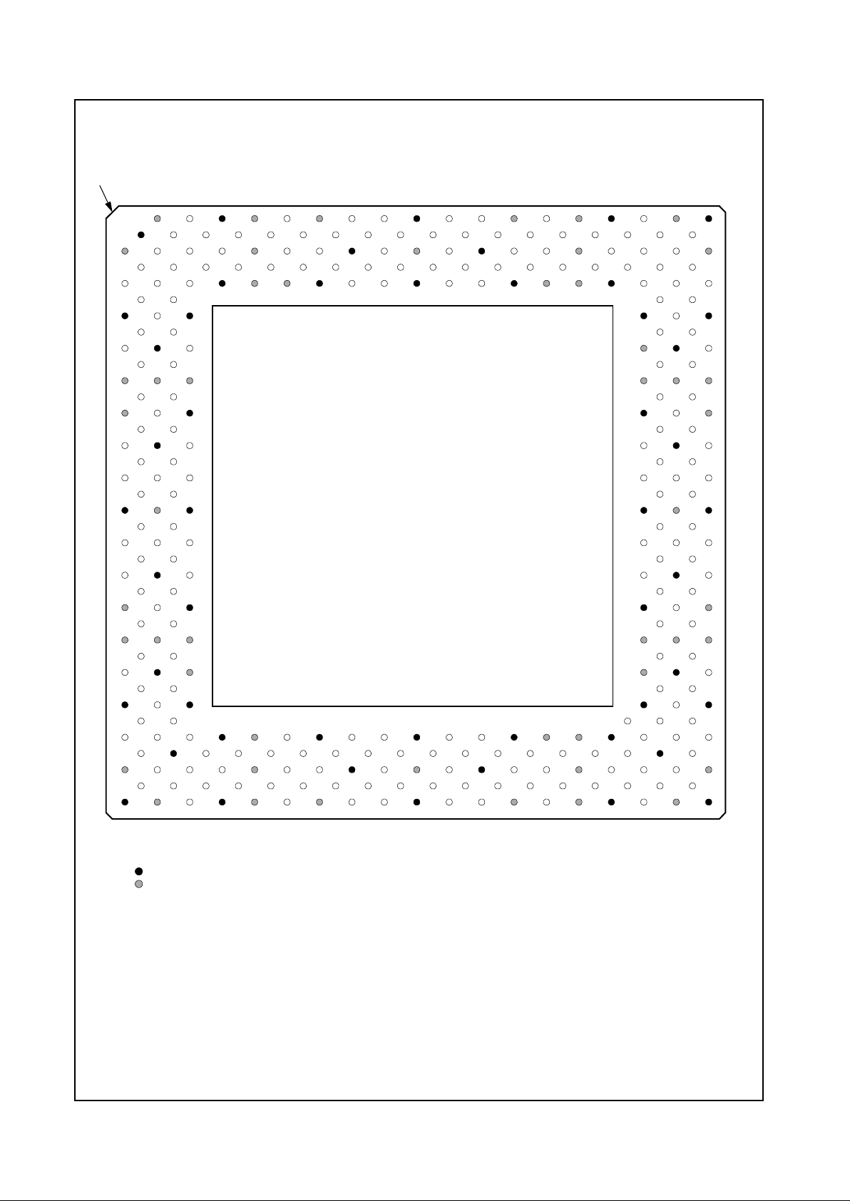
Revision 3.1 19 www.national.com
Signal Definitions (Continued)
Geode™ GXm Processor
Figure 2-3. 320 SPGA Pin Assignment Diagram
For order information refer to Section A.1 “Order Information” on page236.
1234567891011121314151617181920
21 22 23 24 25 26
A
B
C
D
E
F
G
H
J
K
L
M
N
P
Q
R
S
T
U
V
AA
AB
AC
AD
AE
AF
Index Corner
27 28 29 30 31 32 33 34 35 36 37
AG
AH
AJ
AK
AL
AM
W
Y
X
Z
AN
A
B
C
D
E
F
G
H
J
K
L
M
N
P
Q
R
S
T
U
V
AA
AB
AC
AD
AE
AF
AG
AH
AJ
AK
AL
AM
W
Y
X
Z
AN
1234567891011121314151617181920
21 22 23 24 25 26 27 28 29 30 31 32 33 34 35 36 37
VCC3 AD25 VSS VCC2 AD16 VCC3 STOP# SERR# VSS AD11 AD8 VCC3 AD2 VCC2 VSS TST0 VCC3 VSS
VSS AD27 CBE3# AD21 AD19 CBE2# T RDY# LOCK# CBE1# AD13 AD9 AD6 AD3 SMI# AD1 TST2 MD33 MD2
VCC3 AD31 AD26 AD23 VCC2 AD18 FRAM E# VSS PAR VCC3 AD10 VSS AD4 AD0 VCC2 IRQ13 MD1 MD34 VCC3
AD30 AD29 AD24 AD22 AD20 AD17 IRDY# PERR# AD14 AD12 AD7 INTR TST1 TST3 MD0 MD32 MD3 MD35
REQ0# REQ2# AD28 VSS VCC2 VCC2 VSS DEVSEL# AD15 VSS CBE0# AD5 VSS VCC2 VCC2 VSS MD4 MD36 TDN
GNT0# TDI MD5 TDP
VSS CLKMODE2 VSS VSS MD37 VSS
GNT2# SUSPA#
TDO VSS TEST
REQ1# GNT1#
VCC2 VCC2 V CC2
RESET SUSP#
VCC3 TMS V SS
FPVSYN TCK
SERIALP VSS NC
CKMD1 FPHSYN
CKMD0 VID_VAL PIX0
PIX1 PIX2
VSS VCC3 VSS
PIX3 VID_CLK
PIX6 PIX5 PIX4
NC PIX9
PIX8 VSS PIX7
NC PIX10
VCC3 PIX11 VSS
PIX12 PIX13
VCC2 VCC2 V CC2
CRTHSYN DCLK
PIX14 VSS VCC2
PIX15 PIX16
VSS PIX17 VSS
CRTVSYN VDAT6
MD6 MD38
VCC2 VSS MD7
MD39 MD8
VCC2 VCC2 VCC2
MD40 MD9
VSS MD41 VCC3
MD10 MD42
MD11 VSS MD43
MD44 MD12
MD14 MD13 MD45
MD15 MD46
VSS VCC3 VSS
SYSCLK MD47
WEA# WEB# CASA#
DQM0 CASB#
DQM1 VSS DQM4
CS2# DQM5
VSS CS0# VCC3
RASB# RASA#
VCC2 VCC2 VCC2
VCC2 VSS MA1
MA2 MA0
MA4 MA3
VSS MA5 VSS
MA8 MA6MA10
PCLK FLT# VDAT5 VSS VCC2 MD31 VSS MD60 MD57 VSS MD22 MD52 VSS VCC2 VCC2 VSS BA1 MA9 MA7
VRDY VSS VDAT0 SDCLK0 SDCLK2 SDCLKIN MD29 MD27 MD56 MD55 MD21 MD20 MD50 MD16 DQM3 CS3#
VSS BA0
VCC2 VDAT4 VDAT2 SDCLK1 VCC2 RWCLKSDCLKOUT VSS MD58 VCC3 MD23 VSS MD19 MD49 VCC2 DQM6 CKEA MA11 VCC3
VDAT7 VDAT3 ENDIS SDCLK3 MD63 MD30 MD61 MD59 MD25 MD24 MD53 MD51 M D18 MD48 DQM7 DQM2 MA12 VOLDET
VSS VCC2 VDAT1 VSS VCC2 MD62 VCC3 MD28 MD26 VSS MD54 CKEB VCC3 MD17 VCC2 VSS CS1# VCC3 VSS
Note: Signal names have been abbreviated in this figure due to space constraints.
= Denotes GND terminal
= Denotes PWR terminal (VCC2 = VCC_CORE; VCC3 = VCC_IO)
320 SPGA - Top View
Processor
Geode™ GXm
www.national.com 20 Revision 3.1
Signal Definitions (Continued)
Geode™ GXm Processor
Table 2-4. 320 SPGA Pin Assignments - Sorted by Pin Number
Pin
No. Signal Name
A3 VCC3
A5 AD25
A7 VSS
A9 VCC2
A11 AD16
A13 VCC3
A15 STOP#
A17 SERR#
A19 VSS
A21 AD11
A23 AD8
A25 VCC3
A27 AD2
A29 VCC2
A31 VSS
A33 TEST0
A35 VCC3
A37 VSS
B2 VSS
B4 AD27
B6 C/BE3#
B8 AD21
B10 AD19
B12 C/BE2#
B14 TRDY#
B16 LOCK#
B18 C/BE1#
B20 AD13
B22 AD9
B24 AD6
B26 AD3
B28 SMI#
B30 AD1
B32 TEST2
B34 MD33
B36 MD2
C1 VCC3
C3 AD31
C5 AD26
C7 AD23
C9 VCC2
C11 AD18
C13 FRAME#
C15 VSS
C17 PAR
C19 VCC3
C21 AD10
C23 VSS
C25 AD4
C27 AD0
C29 VCC2
C31 IRQ13
C33 MD1
C35 MD34
C37 VCC3
D2 AD30
D4 AD29
D6 AD24
D8 AD22
D10 AD20
D12 AD17
D14 IRDY#
D16 PERR#
D18 AD14
D20 AD12
D22 AD7
D24 INTR
D26 TEST1
D28 TEST3
D30 MD0
D32 MD32
D34 MD3
D36 MD35
E1 REQ0#
E3 REQ2#
E5 AD28
E7 VSS
E9 VCC2
E11 VCC2
E13 VSS
E15 DEVSEL#
E17 AD15
E19 VSS
E21 C/BE0#
E23 AD5
E25 VSS
E27 VCC2
E29 VCC2
E31 VSS
E33 MD4
E35 MD36
E37 TDN
F2 GNT0#
F4 TDI
F34 MD5
F36 TDP
Pin
No. Signal Name
G1 VSS
G3 CLKMODE2
G5 VSS
G33 VSS
G35 MD37
G37 VSS
H2 GNT2#
H4 SUSPA#
H34 MD6
H36 MD38
J1 TDO
J3 VSS
J5 TEST
J33 VCC2
J35 VSS
J37 MD7
K2 REQ1#
K4 GNT1#
K34 MD39
K36 MD8
L1 VCC2
L3 VCC2
L5 VCC2
L33 VCC2
L35 VCC2
L37 VCC2
M2 RESET
M4 SUSP#
M34 MD40
M36 MD9
N1 VCC3
N3 TMS
N5 VSS
N33 VSS
N35 MD41
N37 VCC3
P2 FP_VSYNC
P4 TCLK
P34 MD10
P36 MD42
Q1 SERIALP
Q3 VSS
Q5 NC
Q33 MD11
Q35 VSS
Q37 MD43
R2 CLKMODE1
R4 FP_HSYNC
Pin
No. Signal Name
R34 MD44
R36 MD12
S1 CLKMODE0
S3 VID_VAL
S5 PIXEL0
S33 MD14
S35 MD13
S37 MD45
T2 PIXEL1
T4 PIXEL2
T34 MD15
T36 MD46
U1 VSS
U3 VCC3
U5 VSS
U33 VSS
U35 VCC3
U37 VSS
V2 PIXEL3
V4 VID_CLK
V34 SYSCLK
V36 MD47
W1 PIXEL6
W3 PIXEL5
W5 PIXEL4
W33 WEA#
W35 WEB#
W37 CASA#
X2 NC
X4 PIXEL9
X34 DQM0
X36 CASB#
Y1 PIXEL8
Y3 VSS
Y5 PIXEL7
Y33 DQM1
Y35 VSS
Y37 DQM4
Z2 NC
Z4 PIXEL10
Z34 CS2#
Z36 DQM5
AA1 VCC3
AA3 PIXEL11
AA5 VSS
AA33 VSS
AA35 CS0#
AA37 VCC3
Pin
No. Signal Name
AB2 PIXEL12
AB4 PIXEL13
AB34 RASB#
AB36 RASA#
AC1 VCC2
AC3 VCC2
AC5 VCC2
AC33 VCC2
AC35 VCC2
AC37 VCC2
AD2 CRT_HSYNC
AD4 DCLK
AD34 MA2
AD36 MA0
AE1 PIXEL14
AE3 VSS
AE5 VCC2
AE33 VCC2
AE35 VSS
AE37 MA1
AF2 PIXEL15
AF4 PIXEL16
AF34 MA4
AF36 MA3
AG1 VSS
AG3 PIXEL17
AG5 VSS
AG33 VSS
AG35 MA5
AG37 VSS
AH2 CRT_VSYNC
AH4 VID_DATA6
AH32 MA10
AH34 MA8
AH36 MA6
AJ1 PCLK
AJ3 FTL#
AJ5 VID_DATA5
AJ7 VSS
AJ9 VCC2
AJ11 MD31
AJ13 VSS
AJ15 MD60
AJ17 MD57
AJ19 VSS
AJ21 MD22
AJ23 MD52
AJ25 VSS
Pin
No. Signal Name
Revision 3.1 21 www.national.com
Signal Definitions (Continued)
Geode™ GXm Processor
AJ27 VCC2
AJ29 VCC2
AJ31 VSS
AJ33 BA1
AJ35 MA9
AJ37 MA7
AK2 VID_RDY
AK4 VSS
AK6 VID_DATA0
AK8 SDCLK0
AK10 SDCLK2
AK12 SDCLK_IN
AK14 MD29
AK16 MD27
AK18 MD56
AK20 MD55
AK22 MD21
Pin
No. Signal Name
AK24 MD20
AK26 MD50
AK28 MD16
AK30 DQM3
AK32 CS3#
AK34 VSS
AK36 BA0
AL1 VCC2
AL3 VID_DATA4
AL5 VID_DATA2
AL7 SDCLK1
AL9 VCC2
AL11 RW_CLK
AL13 SDCLK_OUT
AL15 VSS
AL17 MD58
AL19 VCC3
Pin
No. Signal Name
AL21 MD23
AL23 VSS
AL25 MD19
AL27 MD49
AL29 VCC2
AL31 DQM6
AL33 CKEA
AL35 MA11
AL37 VCC3
AM2 VID_DATA7
AM4 VID_DATA3
AM6 ENA_DISP
AM8 SDCLK3
AM10 MD63
AM12 MD30
AM14 MD61
AM16 MD59
Pin
No. Signal Name
AM18 MD25
AM20 MD24
AM22 MD53
AM24 MD51
AM26 MD18
AM28 MD48
AM30 DQM7
AM32 DQM2
AM34 MA12
AM36 VOLDET
AN1 VSS
AN3 VCC2
AN5 VID_DATA1
AN7 VSS
AN9 VCC2
AN11 MD62
AN13 VCC3
Pin
No. Signal Name
AN15 MD28
AN17 MD26
AN19 VSS
AN21 MD54
AN23 CKEB
AN25 VCC3
AN27 MD17
AN29 VCC2
AN31 VSS
AN33 CS1#
AN35 VCC3
AN37 VSS
Pin
No. Signal Name
Table 2-4. 320 SPGA Pin Assignments - Sorted by Pin Number (Continued)
www.national.com 22 Revision 3.1
Signal Definitions (Continued)
Geode™ GXm Processor
Table 2-5. 320 SPGA Pin Assignments - Sorted Alphabetically by Signal Name
Signal Name Type Pin. No.
AD0 I/O C27
AD1 I/O B30
AD2 I/O A27
AD3 I/O B26
AD4 I/O C25
AD5 I/O E23
AD6 I/O B24
AD7 I/O D22
AD8 I/O A23
AD9 I/O B22
AD10 I/O C21
AD11 I/O A21
AD12 I/O D20
AD13 I/O B20
AD14 I/O D18
AD15 I/O E17
AD16 I/O A11
AD17 I/O D12
AD18 I/O C11
AD19 I/O B10
AD20 I/O D10
AD21 I/O B8
AD22 I/O D8
AD23 I/O C7
AD24 I/O D6
AD25 I/O A5
AD26 I/O C5
AD27 I/O B4
AD28 I/O E5
AD29 I/O D4
AD30 I/O D2
AD31 I/O C3
BA0 O AK36
BA1 O AJ33
CASA# O W37
CASB# O X36
C/BE0# I/O E21
C/BE1# I/O B18
C/BE2# I/O B12
C/BE3# I/O B6
CKEA O AL33
CKEB O AN23
CLKMODE0 I S1
CLKMODE1 I R2
CLKMODE2 I G3
CRT_HSYNC O AD2
CRT_VSYNC O AH2
CS0# O AA35
CS1# O AN33
CS2# O Z34
CS3# O AK32
DCLK I AD4
DEVSEL# s/t/s E15 (PU)
DQM0 O X34
DQM1 O Y33
DQM2 O AM32
DQM3 O AK30
DQM4 O Y37
DQM5 O Z36
DQM6 O AL31
DQM7 O AM30
ENA_DISP O AM6
FLT# I AJ3
FP_HSYNC O R4
FP_VSYNC O P2
FRAME# s/t/s C13 (PU)
GNT0# O F2
GNT1# O K4
GNT2# O H2
INTR I D24
IRDY# s/t/s D14 (PU)
IRQ13 O C31
LOCK# s/t/s B16 (PU)
MA0 O AD36
MA1 O AE37
MA2 O AD34
MA3 O AF36
MA4 O AF34
MA5 O AG35
MA6 O AH36
MA7 O AJ37
MA8 O AH34
MA9 O AJ35
MA10 O AH32
MA11 O AL35
MA12 O AM34
MD0 I/O D30
MD1 I/O C33
MD2 I/O B36
MD3 I/O D34
MD4 I/O E33
MD5 I/O F34
MD6 I/O H34
MD7 I/O J37
MD8 I/O K36
MD9 I/O M36
MD10 I/O P34
MD11 I/O Q33
MD12 I/O R36
MD13 I/O S35
MD14 I/O S33
MD15 I/O T34
MD16 I/O AK28
MD17 I/O AN27
MD18 I/O AM26
MD19 I/O AL25
Signal Name Type Pin. No.
MD20 I/O AK24
MD21 I/O AK22
MD22 I/O AJ21
MD23 I/O AL21
MD24 I/O AM20
MD25 I/O AM18
MD26 I/O AN17
MD27 I/O AK16
MD28 I/O AN15
MD29 I/O AK14
MD30 I/O AM12
MD31 I/O AJ11
MD32 I/O D32
MD33 I/O B34
MD34 I/O C35
MD35 I/O D36
MD36 I/O E35
MD37 I/O G35
MD38 I/O H36
MD39 I/O K34
MD40 I/O M34
MD41 I/O N35
MD42 I/O P36
MD43 I/O Q37
MD44 I/O R34
MD45 I/O S37
MD46 I/O T36
MD47 I/O V36
MD48 I/O AM28
MD49 I/O AL27
MD50 I/O AK26
MD51 I/O AM24
MD52 I/O AJ23
MD53 I/O AM22
MD54 I/O AN21
MD55 I/O AK20
MD56 I/O AK18
MD57 I/O AJ17
MD58 I/O AL17
MD59 I/O AM16
MD60 I/O AJ15
MD61 I/O AM14
MD62 I/O AN11
MD63 I/O AM10
NC Q5
NC X2
NC Z2
PAR I/O C17
PCLK O AJ1
PERR# s/t/s D16 (PU)
PIXEL0 O S5
PIXEL1 O T2
PIXEL2 O T4
Signal Name Type Pin. No.
PIXEL3 O V2
PIXEL4 O W5
PIXEL5 O W3
PIXEL6 O W1
PIXEL7 O Y5
PIXEL8 O Y1
PIXEL9 O X4
PIXEL10 O Z4
PIXEL11 O AA3
PIXEL12 O AB2
PIXEL13 O AB4
PIXEL14 O AE1
PIXEL15 O AF2
PIXEL16 O AF4
PIXEL17 O AG3
RASA# O AB36
RASB# O AB34
REQ0# I E1 (PU)
REQ1# I K2 (PU)
REQ2# I E3 (PU)
RESET I M2
RW_CLK O AL11
SDCLK_IN I AK12
SDCLK_OUT O AL13
SDCLK0 O AK8
SDCLK1 O AL7
SDCLK2 O AK10
SDCLK3 O AM8
SERIALP O Q1
SERR# OD A17 (PU)
SMI# I B28
STOP# s/t/s A15 (PU)
SUSP# I M4 (PU)
SUSPA# O H4
SYSCLK I V34
TCLK I P4 (PU)
TDI I F4 (PU)
TDN O E37
TDO O J1
TDP O F36
TEST I J5 (PD)
TEST0 O A33
TEST1 O D26
TEST2 O B32
TEST3 O D28
TMS I N3 (PU)
TRDY# s/t/s B14 (PU)
VCC2 PWR A9
VCC2 PWR A29
VCC2 PWR C9
VCC2 PWR C29
VCC2 PWR E9
VCC2 PWR E11
Signal Name Type Pin. No.
Revision 3.1 23 www.national.com
Signal Definitions (Continued)
Geode™ GXm Processor
Note: PU/PD indicatespin is
internally connected to
a 20-kohm pull-up/
down resistor
VCC2 PWR E27
VCC2 PWR E29
VCC2 PWR J33
VCC2 PWR L1
VCC2 PWR L3
VCC2 PWR L5
VCC2 PWR L33
VCC2 PWR L35
VCC2 PWR L37
VCC2 PWR AC1
VCC2 PWR AC3
VCC2 PWR AC5
VCC2 PWR AC33
VCC2 PWR AC35
VCC2 PWR AC37
VCC2 PWR AE5
VCC2 PWR AE33
VCC2 PWR AJ9
VCC2 PWR AJ27
VCC2 PWR AJ29
VCC2 PWR AL1
VCC2 PWR AL9
VCC2 PWR AL29
VCC2 PWR AN3
VCC2 PWR AN9
VCC2 PWR AN29
VCC3 PWR A3
VCC3 PWR A13
VCC3 PWR A25
Signal Name Type Pin. No.
VCC3 PWR A35
VCC3 PWR C1
VCC3 PWR C19
VCC3 PWR C37
VCC3 PWR N1
VCC3 PWR N37
VCC3 PWR U3
VCC3 PWR U35
VCC3 PWR AA1
VCC3 PWR AA37
VCC3 PWR AL19
VCC3 PWR AL37
VCC3 PWR AN13
VCC3 PWR AN25
VCC3 PWR AN35
VID_CLK O V4
VID_DATA0 O AK6
VID_DATA1 O AN5
VID_DATA2 O AL5
VID_DATA3 O AM4
VID_DATA4 O AL3
VID_DATA5 O AJ5
VID_DATA6 O AH4
VID_DATA7 O AM2
VID_RDY I AK2
VID_VAL O S3
VOLDET O AM36
VSS GND A7
VSS GND A19
Signal Name Type Pin. No.
VSS GND A31
VSS GND A37
VSS GND B2
VSS GND C15
VSS GND C23
VSS GND E7
VSS GND E13
VSS GND E19
VSS GND E25
VSS GND E31
VSS GND G1
VSS GND G5
VSS GND G33
VSS GND G37
VSS GND J3
VSS GND J35
VSS GND N5
VSS GND N33
VSS GND Q3
VSS GND Q35
VSS GND U1
VSS GND U5
VSS GND U33
VSS GND U37
VSS GND Y3
VSS GND Y35
VSS GND AA5
VSS GND AA33
VSS GND AE3
Signal Name Type Pin. No.
VSS GND AE35
VSS GND AG1
VSS GND AG5
VSS GND AG33
VSS GND AG37
VSS GND AJ7
VSS GND AJ13
VSS GND AJ19
VSS GND AJ25
VSS GND AJ31
VSS GND AK4
VSS GND AK34
VSS GND AL15
VSS GND AL23
VSS GND AN1
VSS GND AN7
VSS GND AN19
VSS GND AN31
VSS GND AN37
WEA# O W33
WEB# O W35
Signal Name Type Pin. No.
Table 2-5. 320 SPGA Pin Assignments - Sorted Alphabetically by Signal Name (Continued)

www.national.com 24 Revision 3.1
Signal Definitions (Continued)
Geode™ GXm Processor
2.2 SIGNAL DESCRIPTIONS
2.2.1 System Interface Signals
Signal Name
BGA
Pin No.
SPGA
Pin No. Type Description
SYSCLK P26 V34 I System Clock
System Clock runs synchronouslywiththe PCI bus.The internal
clock of the GXm processor is generated by an internal PLL
which multipliestheSYSCLKinputandcanrun up to eight times
faster. The SYSCLK to core clock multiplier is configured using
the CLKMOD[2:0] inputs.
The SYSCLK input is a fixed frequency which can only be
stopped or varied when the G Xm processoris in a full 3V Suspend. (Section 6.4 “3-Volt SuspendMode” on page 174 for
details regarding this mode.)
CLKMODE[2:0] M1,L1,M3G3,R2,
S1
I Clock Mode
Thesesignalsareusedtosetthecoreclockmultiplier.ThePCI
clock "SYSCLK" is multiplied by the value programmed by CLKMODE[2:0] to generate the GXm processor’s core clock.
CLKMODE2isvalid only forGXmprocessor revision 4.0 and up.
The value read from DIR1 (Device ID Register 1, refer to
page 51) affects the definition of the CLKMODE pins.
If DIR1 = 30h-33h then CLKMODE[1:0]:
00 = SYSCLK multiplied by 4 (Test mode only)
01 = SYSCLK multiplied by 6
10 = SYSCLK multiplied by 7
11 = SYSCLK multiplied by 5
If DIR1 = 34h-4Fh then CLKMODE[1:0]:
00 = SYSCLK multiplied by 4 (Test mode only)
01 = SYSCLK multiplied by 6
10 = SYSCLK multiplied by 7
11 = SYSCLK multiplied by 8
If DIR1 > or = 50h then CLKMODE[2:0]:
000 = SYSCLK multiplied by 4 (Test mode only)
001 = SYSCLK multiplied by 10
010 = SYSCLK multiplied by 9
011 = SYSCLK multiplied by 5
100 = SYSCLK multiplied by 4
101 = SYSCLK multiplied by 6
110 = SYSCLK multiplied by 7
111 = SYSCLK multiplied by 8
RESET J3 M2 I Reset
RESET aborts all operationsin progress and places the
GXm processor into a reset state. RESET forces the CPU and
peripheralfunctionstobeginexecutingataknownstate. All data
in the on-chip cache is invalidated.
RESET is an asynchronous input but must meet specified setup
and hold times to guarantee recognition at a particular clock
edge. This input is typically generated during the Power-OnReset sequence.
Note: Warm Reset does not require an input on the GXm pro-
cessor since the function is virtualized using SMM.

Revision 3.1 25 www.national.com
Signal Definitions (Continued)
Geode™ GXm Processor
INTR B18 D24 I (Maskable) Interrupt Request
INTR is a level-sensitiveinputthatcauses the GXm processor to
Suspend execution of the currentinstruction stream and begin
execution of an interrupt service routine. The INTR input can be
masked through the Flags Register IF bit. (See Table3-4 on
page 43 for bit definitions.)
IRQ13 C22 C31 O Interrupt Request Level 13
IRQ13 is asserted if an on-chip floating point error occurs.
When a floating point error occurs,the GXm processor asserts
the IRQ13 pin. The floating point interrupt handler then performs
an OUT instruction to I/O address F0h or F1h. The GXmprocessor accepts either of these cycles and clearsthe IRQ13 pin.
Refer to Section 3.4.1 “I/O Address Space” on page 60 for further information on IN/OUT instructions.
SMI# C19 B28 I System Management Interrupt
SMI# is a level-sensitiveinterrupt. SMI# puts the GXm processor
into System Management Mode (SMM).
SUSP# H2
(PU)
M4
(PU)
I Suspend Request
This signal is used to request that the GXm processor enter Suspend mode. After recognition of an active SUSP# input, theprocessor completes execution of the current instruction, any
pending decoded instructions and associated bus cycles.
SUSP# is ignored following RESET# and is enabledby setting
the SUSP bit in CCR2. (See Table 16 on page 44 for CCR2 bit
definitions.)
SincetheGXmprocessor includessystemlogic functionsaswell
as the CPU core, there are specialmodesdesignedto support
the different power management states associated with APM,
ACPI, and portable designs. The part can be configured to stop
only the CPU core clocks, or all clocks. When all clocks are
stopped, the external clock can also be stopped.(See Section
6.0 “PowerManagement” onpage174 for moredetailsregarding
power management states.)
This pin is internally connected to a 20-kohm pull-up resistor.
SUSP#ispulledupwhennotactive.
SUSPA# E2 H4 O Suspend Acknowledge
Suspend Acknowledge indicates that the GXm processor has
entered low-power Suspend mode as a result of SUSP# assertion or execution of a HALTinstruction.SUSPA# is enabled by
setting the SUSP bit in CCR2. (See Table 16 on page 44 for
CCR2 bit definitions.)
The SYSCLK input may be stopped after SUSPA# has been
asserted to further reduce power consumption if the system is
configured for 3V Suspend mode. (Section 6.4 “3-VoltSuspend
Mode” on page 174 for details regarding this mode.)
SERIALP L3 Q1 O Serial Packet
Serial Packet is the singlewire serial-transmission signal to the
CS5530 chip. The clock used for this interface is the PCI clock
(SYSCLK). This interface carries packets of miscellaneous information to the chipset to be used by the VSA software handlers.
2.2.1 System Interface Signals (Continued)
Signal Name
BGA
Pin No.
SPGA
Pin No. Type Description

www.national.com 26 Revision 3.1
Signal Definitions (Continued)
Geode™ GXm Processor
2.2.2 PCI Interface Signals
Signal Name
BGA
Pin No.
SPGA
Pin No Type Description
AD[31:0] Refer
toTable
2-3
Refer
toTable
2-5
I/O Multiplexed Address and Data
Addressesanddata are multiplexed onthesame PCI pins. Abus
transaction consists of an address phase in the cycle in which
FRAME# is asserted followed by one or more data phases. During the address phase, AD[31:0] contain a physical 32-bit
address. For I/O,this is a byte address, for configuration and
memory it is a DWORD address. During data phases, AD[7:0]
contain the least significant byte (LSB) and AD[31:24]contain
the most significant byte (MSB). Write data is stable and valid
when IRDY# is asserted and read data is stable and valid when
TRDY# is asserted. Data is transferred during those SYSCLKS
where both IRDY# and TRDY# are asserted.
C/BE[3:0]# D5,
B8,
C13,
A15
B6,
B12,
B18,
E21
I/O Multiplexed Command and Byte Enables
Bus command and byte enables are multiplexed on the same
PCI pins. During the address phase of a transactionwhen
FRAME# is active, C/BE[3:0]# define the bus command. During
the data phase C/BE[3:0]# are used as byte enables. The byte
enables are valid for the entire data phase and determinewhich
byte lanes carry meaningful data. C/BE0#appliesto byte 0
(LSB) and C/BE3# appliesto byte 3 (MSB).
The command encoding and types are listedbelow.
0000 = Interrupt Acknowledge
0001 = Special Cycle
0010 = I/O Read
0011 = I/O Write
0100 = Reserved
0101 = Reserved
0110 = Memory Read
0111 = Memory Write
1000 = Reserved
1001 = Reserved
1010 = Configuration Read
1011 = Configuration Write
1100 = Memory ReadMultiple
1101 = Dual Address Cycle (Reserved)
1110 = Memory ReadLine
1111 = Memory Write and Invalidate
PAR B12 C17 I/O Parity
Paritygeneration is required by all PCIagents:themasterdrives
PARfor addressandwrite-dataphases, the target drivesPAR for
read-data phases. Parity is even across AD[31:0] and
C/BE[3:0]#.
For address phases, PAR is stable and valid one SYSCLK after
the address phase. It has the same timing as AD[31:0] but
delayedby one SYSCLK.
For data phases, PAR is stable and valid one SYSCLK after
either IRDY# is asserted on a write transaction or after TRDY#is
asserted on a read transaction. Once PAR is valid, it remains
valid until one SYSCLK after the completion of the data phase.
(Also see PERR#.)

Revision 3.1 27 www.national.com
Signal Definitions (Continued)
Geode™ GXm Processor
FRAME# A8
(PU)
C13
(PU)
s/t/s Frame
Cycle Frameis driven by the current master to indicate the
beginning and duration of an access. FRAME# is asserted to
indicate a bus transaction is beginning. While FRAME# is
asserted, data transfers continue. When FRAME# is deasserted,
the transaction is in the final data phase.
This pin is internally connected to a 20-kohm pull-up resistor.
IRDY# C9
(PU)
D14
(PU)
s/t/s Initiator Ready
Initiator Ready is asserted to indicate that the bus master is able
to complete the current data phaseof the transaction. IRDY# is
used in conjunction with TRDY#. A data phase is completed on
any SYSCLK in which both IRDY# and TRDY# are sampled
asserted. During a write, IRDY# indicates valid data is present
on AD[31:0]. Duringaread,itindicatesthe master is prepared to
accept data. Wait cycles are inserted until bothIRDY# and
TRDY# are asserted together.
This pin is internally connected to a 20-kohm pull-up resistor.
TRDY# B9
(PU)
B14
(PU)
s/t/s Target Ready
TRDY# is asserted to indicate that the target agent is able to
complete the current data phase of the transaction.TRDY# is
usedinconjunction withIRDY#. A data phaseiscomplete on any
SYSCLK in which both TRDY# and IRDY# are sampled
asserted. During a read, TRDY# indicates that valid data is
present on AD[31:0]. During a write, it indicates the target is prepared to accept data. Wait cycles are inserted until both IRDY#
and TRDY#are asserted together.
This pin is internally connected to a 20-kohm pull-up resistor.
STOP# C11
(PU)
A15
(PU)
s/t/s Target Stop
STOP# is asserted to indicatethat the current target is requesting the mastertostopthecurrent transaction. This signalisused
with DEVSEL# to indicateretry, disconnect or target abort. If
STOP# is sampled active while a master, FRAME# will be deasserted and the cycle stoppedwithinthree SYSCLK cycles. As an
input, STOP# can be asserted in the following cases. 1) If a PCI
master tries to access memory that has been locked by another
master. This condition is detectedif FRAME# and LOCK# are
asserted during an addressphase. 2) STOP# will also be
asserted if the PCI write buffers are full or ifapreviously buffered
cycle has not completed. 3) Finally, STOP# can be asserted on
read cycles that cross cache line boundaries. This is conditional
based upon the programming of bit 1 in PCI Control Function 2
Register. (See Table 4-37 on page 156 forprogramming details.)
This pin is internally connected to a 20-kohm pull-up resistor.
2.2.2 PCI Interface Signals (Continued)
Signal Name
BGA
Pin No.
SPGA
Pin No Type Description

www.national.com 28 Revision 3.1
Signal Definitions (Continued)
Geode™ GXm Processor
LOCK# B11
(PU)
B16
(PU)
s/t/s Lock Operation
LOCK# indicates an atomic operation that may require multiple
transactions to complete. When LOCK# is asserted, nonexclusivetransactions may proceedtoanaddressthatisnotcurrently
locked(atleast 16 bytes must be locked). A grant to start a transaction on PCI does not guarantee control of LOCK#. Control of
LOCK# is obtained under it own protocol in conjunction with
GNT#. It is possible fordifferent agents to use PCI while a single
master retains ownership of LOCK#. The arbiter can implement
a complete system lock. In this mode, if LOCK# is active, no
other master can gain access to the systemuntil the LOCK# is
deasserted.
This pin is internally connected to a 20-kohm pull-up resistor.
DEVSEL# A9
(PU)
E15
(PU)
s/t/s Device Select
DEVSEL# indicates that the drivingdevice has decoded its
address as the target of the current access. As an input,
DEVSEL# indicates whether any device on the bus has been
selected. DEVSEL# will also be driven by any agent that has the
ability to accept cycles on a subtractive decode basis. As a master,if no DEVSEL# is detected withinand up to the subtractive
decode clock, a master abort cyclewill result expectfor special
cycles which do not expecta DEVSEL# returned.
This pin is internally connected to a 20-kohm pull-up resistor.
PERR# A11
(PU)
D16
(PU)
s/t/s Parity Error
PERR# is used for repor ting of data parity errors during all PCI
transactions except a Special Cycle. The PERR# line is driven
two SYSCLKs after the data in which the error was detected.
This is one SYSCLK after the PAR that is attached to the data.
The minimum duration of PERR# is one SYSCLK for each data
phase in which a data parity error is detected. PERR# mustbe
driven highforoneSYSCLKbefore being in TRI-STATE mode. A
target asserts PERR# onwrite cycles if it has claimed the cycle
with DEVSEL#. The masterasserts PERR# on read cycles.
This pin is internally connected to a 20-kohm pull-up resistor.
SERR# C12
(PU)
A17
(PU)
OD System Error
System Error may be asserted by any agent for repor ting errors
other than PCI parity. The intent is to have the PCI c entral agent
assert NMI to the processor. When the Parity Enable bit is set in
the Memory Controller Configuration register, SERR# will be
asserted upon detecting a parity error on read operations from
DRAM.
REQ[2:0]# D3,
H3,
E3
(PU)
E3,
K2,
E1
(PU)
I Request Lines
Request indicates to the arbiter that an agent desires use of the
bus. Each master has its own REQ# line. REQ# priorities are
based on the arbitration scheme chosen.
Each of these pins are internallyconnected to a 20-kohm pull-up
resistor.
2.2.2 PCI Interface Signals (Continued)
Signal Name
BGA
Pin No.
SPGA
Pin No Type Description

Revision 3.1 29 www.national.com
Signal Definitions (Continued)
Geode™ GXm Processor
GNT[2:0]# E1,
F2,
D1
H2,
K4,
F2
O Grant Lines
Grant indicatesto therequesting master that it has been granted
access to the bus. Each master has its own GNT# line. GNT#
can be pulled away at any time a higher REQ#is receivedor if
the master does not begin a cycle within a minimum period of
time (16 SYSCLKs).
2.2.2 PCI Interface Signals (Continued)
Signal Name
BGA
Pin No.
SPGA
Pin No Type Description
2.2.3 Memory Controller Interface Signals
Signal Name
BGA
Pin No.
SPGA
Pin No. Type Description
Note: The memory controller interface supports two typesof memory configurations: SDRAM modules on the sys-
tem board and JEDEC DIMMconnectors. Refer to Section 4.3 “Memory Controller” on page 103 for detailed
information regarding signal connections.
MD[63:0] Refer
toTable
2-3
Refer
toTable
2-5
I/O Memory Data Bus
The data bus lines driven to/from system memory.
MA[12:0] Refer
toTable
2-3
Refer
toTable
2-5
O Memory Address Bus
The multiplexed row/column address lines driven to the system
memory.
Supports 256 Mbit SDRAM.
BA[1:0] AD26,
AD25
AJ33,
AK36
O Bank Address Bits
These bits are used to select the component bank within the
SDRAM.
CS[3:0]# AE23,
V25,
AD23,
V26
AK32,
Z34,
AN33,
AA35
O Chip Selects
The chip selects are used to select the module bank within the
system memory. Eachchipselect corresponds to a specific module bank.
If CS# is high, the bank(s) do not respond to RAS#, CAS#, WE#
until the bank is selected again.
RASA#,
RASB#
W24,
W25
AB36,
AB34
O Row Address Strobe
RAS#, CAS#, WE# and CKE are encoded to support the different SDRAM commands. RASA# is used with CS[1:0]#. RASB#
is used with CS[3:2]#.
CASA#,
CASB#
P25,
R26
W37,
X36
O Column Address Strobe
RAS#, CAS#, WE# and CKE are encoded to support the different SDRAM commands. CASA# is used with CS[1:0]#. CASB#
is used with CS[3:2]#.
WEA#,
WEB#
R25,
R24
W33,
W35
O Write Enable
RAS#, CAS#, WE# and CKE are encoded to support the different SDRAM commands. WEA# is used with CS[1:0]#. WEB# is
used with CS[3:2]#.

www.national.com 30 Revision 3.1
Signal Definitions (Continued)
Geode™ GXm Processor
DQM[7:0] Refer
toTable
2-3
Refer
toTable
2-5
O Data Mask Control Bits
During memory read cycles, these outputs control whether the
SDRAM output buffers are driven on the MD busornot.AllDQM
signals are asserted during read cycles.
During memory write cycles, these outputs control whether or
not MD data will be written into the SDRAM.
DQM[7:0] connect directly to the DQM7-0 pins of eachconnector.
CKEA,
CKEB
AF24,
AD16
AL33,
AN23
O Clock Enable
For normal operation CKE is held high. CKE goes low during
Suspend.
SDCLK[3:0] AE4,
AF5,
AE5,
AF4
AM8,
AK10,
AL7,
AK8
O SDRAM Clocks
The SDRAM samples all the control,address, and data using
these clocks.
SDCLK_IN AE8 AK12 I SDRAM Clock Input
The GXm processor samples the memory read data on this
clock. Works in conjunction with the SDCLK_OUT signal.
SDCLK_OUT AF8 AL13 O SDRAM Clock Output
This output is routed back to SDCLK_IN. The board designer
should vary the length of the board trace to control skew
between SDCLK_IN and SDCLK.
2.2.3 Memory Controller Interface Signals (Continued)
Signal Name
BGA
Pin No.
SPGA
Pin No. Type Description
2.2.4 Video Interface Signals
Signal Name
BGA
Pin No
SPGA
Pin No Type Description
PCLK AC1 AJ1 O Pixel Port Clock
Pixel Port Clock represents the pixel dotclock or a 2x multiple of
the dotclock for some 16-bit-per-pixel modes. It determines the
data transfer rate from the GXm processor to the CS5530.
VID_CLK P1 V4 O Video Clock
Video Clock represents the video port clock to the CS5530. This
pin is only used if the Video Port is enabled.
DCLK AB1 AD4 I DOT Clock
The DCLK input is driven from the CS5530and represents the
pixel dot clock. In some cases, such as when displaying 16 BPP
data with an eight-bit-graphics pixel port, this clock will actually
be a 2x multiple of the dotclock.
CRT_HSYNC W2 AD2 O CRT Horizontal Sync
CRT Horizontal Sync establishes the line rateand horizontal
retrace interval for an attached CRT. The polarity is programmable and depends on the display mode.
 Loading...