NSC FPD85310VJD, FLINK3V-TCON Datasheet
FPD85310
Panel Timing Controller
General Description
The FPD85310 Panel Timing Controller is an integrated
FPD-Link based TFT-LCD timing controller. It resides on the
flat panel display and provides the interface signal routing
and timing control betweengraphicsor video controllers and
a TFT-LCD system. FPD-Link is a low power, low electromagnetic interference interface used between this controller
and the host system.
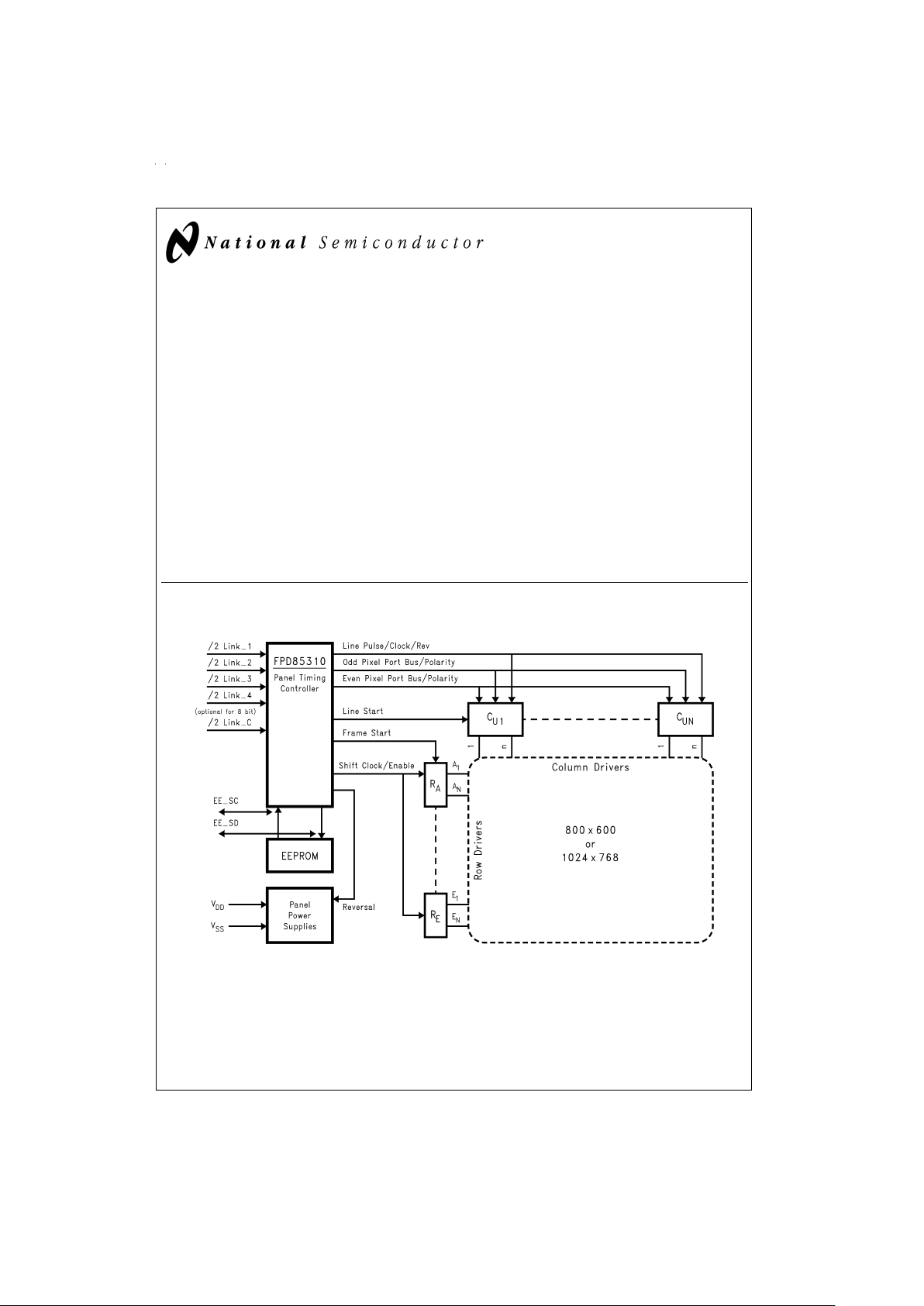
The FPD85310 chip links the panel’s system interface to the
display via a ten wire LVDS data bus. That data is then
routed to the source and gate display drivers. XGA and
SVGA resolutions are supported.
The FPD85310 is programmable via an optional external serial EEPROM. Reserved space in the EEPROM is available
for display identification information. The system can access
the EEPROM to read the display identification data or program initialization values used by the FPD85310.
Features
n FPD-Link System Interface utilizes Low Voltage
Differential Signaling (LVDS).
n System programmable via EEPROM
n Suitable for notebook and monitor applications
n 8-bit or 6-bit system interface
n XGA or SVGA capable
n Supports single or dual port column drivers
n Programmable outputs provide customized control for
standard or in-house column drivers and row drivers
n Fail-safe operation prevents panel damage with system
clock failure
n Programmable skew rate controlled outputs on CD
interface for reduced EMI
n Polarity pin reduces CD data bus switching
n CMOS circuitry operates from a 3.3V supply
System Diagram
TRI-STATE®is a registered trademark of National Semiconductor Corporation.
DS101086-1
September 1999
FPD85310 Panel Timing Controller
© 1999 National Semiconductor Corporation DS101086 www.national.com
Absolute Maximum Ratings (Note 1)
If Military/Aerospace specified devices are required,
please contact the National Semiconductor Sales Office/
Distributors for availability and specifications.
Supply Voltage (V
DD
) 4.1V
DC Input Voltage (V
IN
) −0.5V to VDD+0.5V
DC Output Voltage (V
OUT
) −0.5V to VDD+0.5V
Storage Temperature Range
(T
STG
) −65˚C to +150˚C
Lead Temperature (T
L
)
(Soldering 10 sec.) 260˚C
ESD Rating:
(C
ZAP
= 120 pF, R
ZAP
= 1500Ω)
MM=200V, HBM=2000V
Operating Conditions
Min Max Units
Supply Voltage (V
DD
) 3.0 3.6 V
Operating Temp. Range (T
A
) 0 70 ˚C
Note 1: “Absolute Maximum Ratings” are those values beyond which the
safety of the device cannot be guaranteed. They are not meant to imply that
the devices should be operated at these limits. The table of “Electrical Characteristics” specifies conditions of device operation.
DC Electrical Characteristics T
A
=
0˚C to 70˚C, V
DD
=
3.3V
±
0.3V (unless otherwise specified)
Symbol Parameter Conditions Min Max Units
V
OH
Minimum High Level
Output Voltage
VDD= 3.0V, IOH= 1 mA 2.4 V
V
OL
Maximum Low Level
Output Voltage
VDD= 3.0V, IOL= 1 mA 0.4 V
V
IH
Minimum High Level
Input Voltage
2.0 V
V
IL
Maximum Low Level
Input Voltage
0.8 V
I
IN
Input Current VIN=V
DD
10 µA
I
OZ
Maximum TRI-STATE
Output Leakage Current
VIN=VDD,VIN=V
SS
10 µA
I
DD
Average Supply Current f=65 MHz, C
LOAD
= 50 pF 312 mA
V
THH
Differential Input High
Threshold
Common Mode Voltage = +1.2V +100 mV
V
THL
Differential Input Low
Threshold
Common Mode Voltage = +1.2V -100 mV
Device Specifications T
A
=
0˚C to 70˚C, V
DD
=
3.3V (unless otherwise specified)
Symbol Parameter Conditions Min Max Units
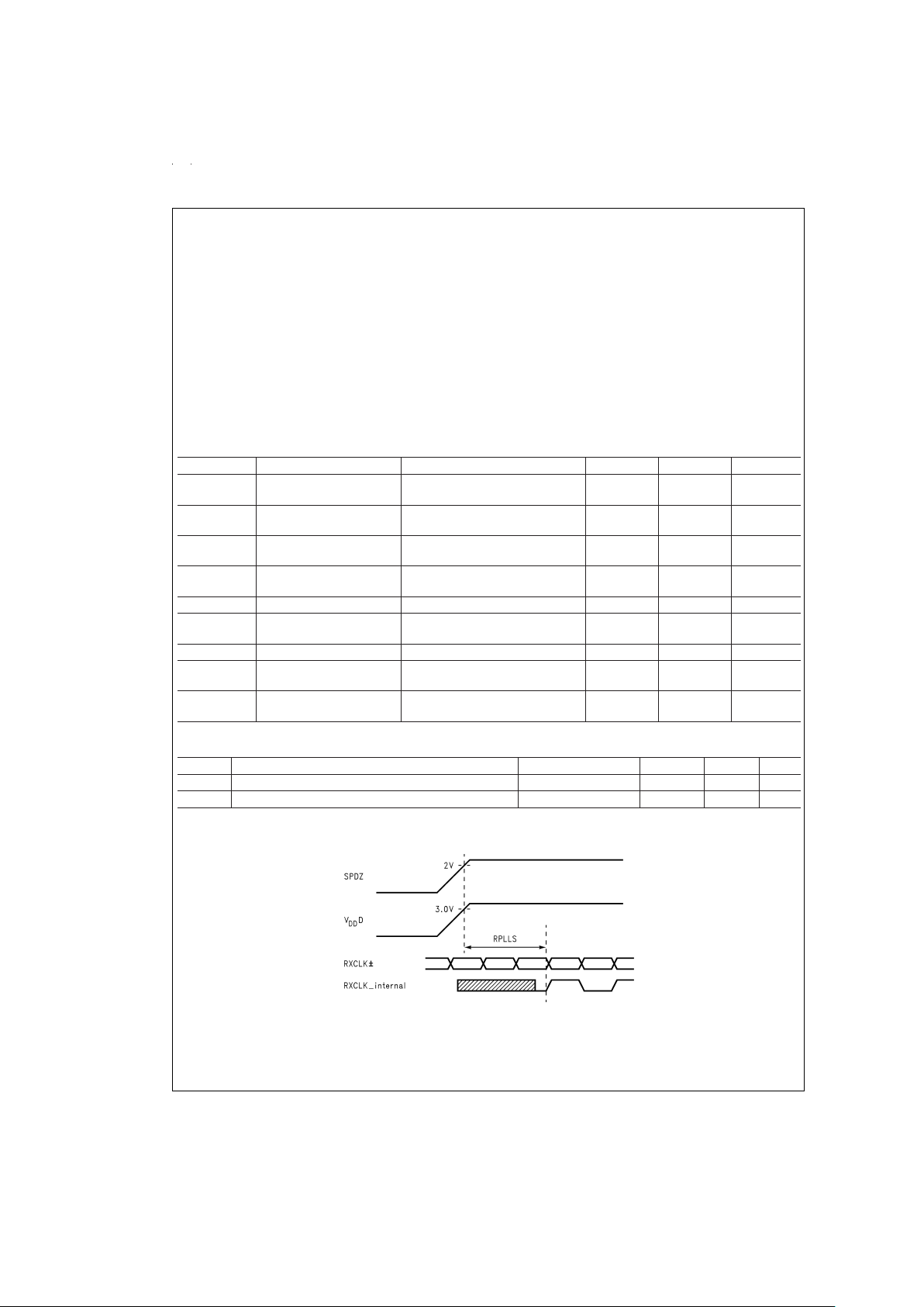
RPLLS Receiver Phase Lock Loop Set Time 10 ms
RCCS RxIN Channel-to-Channel Skew (Note 2) 700 ps
Note 2: This limit assumes a maximum cable skew of 350 ps. Actual automated test equipment limit is 400 ps due to tester accuracy.
DS101086-12
FIGURE 1. FPD85310 (Receiver) Phase Lock Loop Set Time
www.national.com 2
Device Specifications T
A
=
0˚C to 70˚C, V
DD
=
3.3V (unless otherwise specified) (Continued)
Symbol Parameter Conditions Min Max Units
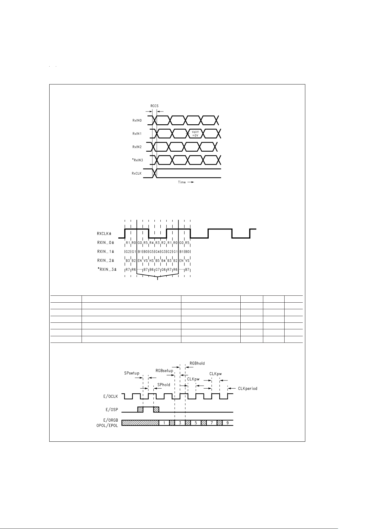
SPsetup E/OSP from E/OCLK 65 MHz Video (Note 6) 8 ns
SPhold E/OSP from E/OCLK 65 MHz Video (Note 6) 8 ns
RGBsetup ER/EG/EB/OR/OG/OB from E/OCLK 65 MHz Video (Note 6) 8 ns
RGBhold ER/EG/EB/OR/OG/OB from E/OCLK 65 MHz Video (Note 6) 8 ns
CLKpw E/OCLK pulsewidth 65 MHz Video (Note 6) 11 ns
CLKperiod E/OCLK period 65 MHz Video (Note 6) 25 ns
Note 6: Timing applies to Dual Bus output modes.
DS101086-13
Note 3: Measurements at V
DIFF
=0V
Note 4: RCCS measured between earliest and latest LVDS edges
Note 5:
*
RxIN3 pair (RxIN_3±) is option for 24-bit color depth
FIGURE 2. FPD85310 (Receiver) Channel-to-Channel Skew and Pulse Width
DS101086-14
FIGURE 3. FPD85310’s (Receiver) Format of the Input Data
DS101086-15
FIGURE 4. Column Driver Bus AC Timing
www.national.com3
Device Specifications T
A
=
0˚C to 70˚C, V
DD
=
3.3V (unless otherwise specified) (Continued)
DS101086-16
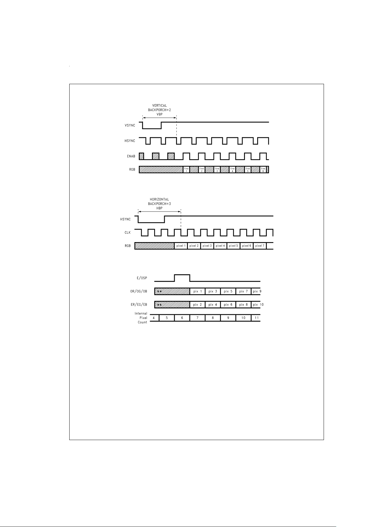
FIGURE 5. Vertical Backporch Definition
(Video Data from Host)
DS101086-17
FIGURE 6. Horizontal Backporch Definition
(Video Data from Host)
DS101086-18
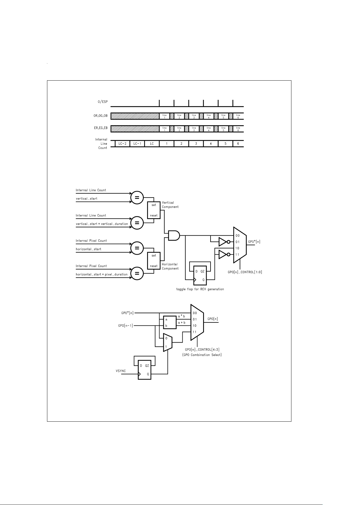
Internal Pixel Count final value = pixels per line/2
Maximum Internal Pixel Count = 1024 (32.5 MHz clocks)
Internal Pixel Count is used to generate the horizontal_component for GPO generation
See
Figure 9
**
Without Blanking control (GPO8), random data may be observed during 16 OCLK and discontinuous 1 OCLK before E/OSP, but it should not be affected to
actual image.
FIGURE 7. Internal Pixel Count Used for GPO Control Generation
www.national.com 4
Device Specifications T
A
=
0˚C to 70˚C, V
DD
=
3.3V (unless otherwise specified) (Continued)
DS101086-19
LC = lines per frame count, LCmax = 2048 lines
Internal Line Count is used to generate the vertical component for GPO generation
See
Figure 9
FIGURE 8. Internal Line Count Used for GPO Control Generation
GPO Generation
DS101086-20
GPO Combination Select
DS101086-21
FIGURE 9. GPO Control Generation
www.national.com5
Device Specifications T
A
=
0˚C to 70˚C, V
DD
=
3.3V (unless otherwise specified) (Continued)
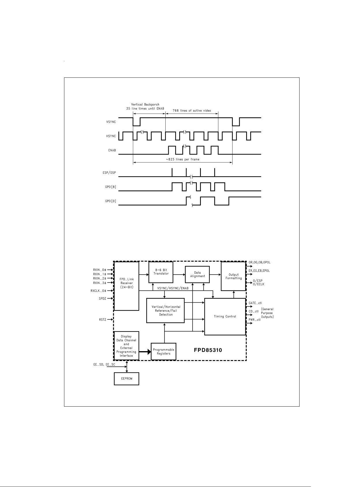
Block Diagram
FPD85310 Default Timing
DS101086-22
Vertical Backporch=35
Lines/Frame=∼825
Pixels/Line=∼1200
Horizontal Backporch=∼100
Displayed pixels/line=1024
(Valid data during ENAB High time)
Displayed lines/frames=768
Frequency=65 MHz (or less)
DS101086-3
www.national.com 6

Functional Description
FPD-LINK RECEIVER
The LVDS based FPD-Link Receiver receives inputs video
data and control timing. Four LVDS channels plus clock provide 24-bit color. Three LVDS channels can be used for
18-bit color.
The video data is regenerated to a parallel data stream and
routed to the 8 to 6 Bit Translator.When SPDZ is active (low)
the FPD85310 is placed in a power down mode. The General Purpose Outputs (GPOs) continue outputting the programmed control sequence at a reduced frame rate. RSTZ
initialized the chip with the default register values. EEPROM
configuration data is loaded if EEPROM is detected. (EEPROM address 80H=“00”).
8 to 6 Bit Translator
8-bit data is reduced to a 6-bit data path via a time multiplexed dithering technique or a simple truncation of the
LSBs. This function is enabled via the Input Control Register
bits 4 and 3. See
Table 2
Input Format Control register.
DATA ALIGNMENT
This function delays and aligns data to match the CD/panel
architect. The following programmable selections in the Output Format Control Register bits 0 and 1 provide support for
various panel architectures. See
Figures 10, 11, 12, 13, 14
for additional explanation.
Dual Bus, Single Port CD Interface
When interfacing two busses to a bank of single port column
drivers, the RGB data must be aligned/delayed with respect
to the size of the column drivers being used. The CD Size
register is programmed to support single port column drivers
of up to 384 outputs (128 pixels).
Dual Bus, Dual Port CD Interface
When interfacing with dual port column drivers, data is simply output with odd and even data on separate outputs.
Single Bus, Single Port CD Interface
The single bus, single port column driver interface provides
support of existing SVGA systems. All data is output on a
single bus. The second bus can be turned off when using
this configuration.
Output Formatting
The output formatting function provides several capabilities
to reduce noise EMI and to generate customized timing.
These capabilities are selectable/programmable via the Output Format Control, Output Enable/Polarity Control, and Output Drive Control Registers. See
Table2
for specific bit defi-
nitions.
Data Bus Skewing
This function aligns the two output channels in either a nonskewed data format (simultaneous switching) or a skewed
data format. The skewed format delays the even channel
data and control by
1
⁄2clock. This reduces the number of out-
puts which switch simultaneously. See
Figures 10, 11, 12,
13, 14
. Data Bus Skewing is enabled by setting bit 2 in the
Output Format Control register.
Programmable Skew Rates
Programmable edge rates allow the Data, Polarity, Start
Pulse, and Clock outputs to be adjusted for better impedance matching for noise and EMI reduction. Bits [7:6] of the
Output Enable/Polarity Control Register control OSP and
ESP outputs. The Output Drive Control register control the
OCLK, ECLK, ORGB/OPOL, ERGB/EPOL outputs.
Polarity Generation
When enabled, a polarity indication is output for each data
bus. If the number of transitions from pixel to pixel exceed 18
bits from 36 bits, the data is inverted and a polarity indication
corresponding to that bus is set active. This requires the use
of a CD with a polarity input and in “SKEWED” mode, OPOL
and EPOL are separated for each skewing then two port CD
need to be two polarity inputs. Polarity Generation is not supported in the single bus/single port CD configuration (SVGA
configuration). The polarity function is enabled by setting bit
6 of the Output Format Control register (EEPROM address
D2). The OCLK and ECLK polarity is also programmable. Inversion and TRI-STATE control of OCLK and ECLK is provided by bits [3:0] of the Output Enable/Polarity Control Register. The ERGB/ESP/EPOL and ORGB/OSP/OPALoutputs
can be disabled (TRI-STATE) using bits [5:4] of the Output
Enable/Polarity Control register.
Programmable Positioning of CD Start Pulse
The position of the CD Start Pulse is programmable. This allows use with column drivers having non-standard start
pulse timing. The CD Start Pulse position is determined by
bits [3:0] of the Output Format Control Register (EEPROM
address D3).
Data Blanking
Data, Polarity,Start Pulse and Clock can be blanked (forced
to “0”) during horizontal and/or vertical blanking periods.
GPO [8] is programmed to correspond to display periods.
When GPO [8] is low, outputs are forced to “0”. This reduces
amount of switching over the frame time thus reducing
power. See GPO programming procedure in
APPENDIX A:
GPO Programming Examples
.
Line Inversion
When enabled (Bit 3 of the Output Format Register), the polarity of the output data is determined by GPO [0]. Bit 4 defines the relationship between GPO [0] and the output data.
Bit 5 provides a variation of this where the Odd and Even
data is of different polarity. This could be used in a system
with CDs on both top and bottom of the panel in which dot inversion is desired.
White Data
The White Data function generates all “1” data beginning at
line 769 and continuing until the beginning of the next frame.
This function is controlled via D6 Register Bit 7.
Timing Control
The Timing Control function generates control to column
drivers, row drivers, and power supply. The programmable
GPOs provide for CD latch pulse, REV,and gate driver control generation. The GPOs allow the user to generate control
anywhere within the frame data. Standard gate driver inter-
www.national.com7

Functional Description (Continued)
face or custom gate interfaces can be implemented with the
nine GPOs. Note that GPO [8] must be used for output
blanking control.
Five registers provide the timing definition for each GPO.
The Horizontal Start register defines the output pixel number
for which the GPO output goes active. The Horizontal duration register determines how many clocks the output will remain active during the line. The VerticalStart register defines
at what line # the output becomes active, and the Vertical duration register defines how many lines the output remains
active. Each output has a control register (bit 0) which defines the GPO polarity (active high or low). Another bit in the
control register (bit 1) enables the “toggle” mode. This mode
is useful in REV generation when alternating polarity is required from line to line. Frame to Frame polarity changes are
made by programming an odd # in the vertical duration register when in “toggle” mode.
Two of the General Purpose Outputs have additional capabilities. GPO [8] controls output blanking and must be used
for this purpose. If output blanking is not desired, this register
must be programmed to always be active. White data generation (all “1” data) at the end of each frame is generated
when D6 register bit 7 is set. When this bit is set, white data
is output after line #768 if GPO [8] is active. GPO [0] is capable of performing line inversion on the output data. Bits
[5:3] of the Output Format Control register provides control
for this function.
See
APPENDIX A: GPO Programming Examples
.
SERIAL EEPROM INTERFACE
The Serial EEPROM Interface controls the FPD85310 initialization. If the EEPROM is not present (EESD and EESC are
pulled high), or if EEPROM address 80H is not “00”, the internal default values are used to initialize all programmable
functions of the FPD85310.
At power-up, the FPD85310 configures the internal programmable registers with data from the EEPROM. After the
FPD85310 is initialized, the EEPROM can be accessed by
the system in which display configuration and manufacturing
information can be obtained. The EEPROM can be programmed “in system” providing quick evaluation of different
display timing.
External access to the EEPROM must be preceded by applying a “1” to pin TEST [2] in order to interrupt the
FPD85310 download.
The FPD85310 initialization data begins at EEPROM address 80H. The first 128 bytes (0-7F) are reserved for display identification data.
A power-up delay can be programmed using bits [6:5] of the
Input Format Control Register. This delays outputting (driving) of the data and control for up to 5 frame times after reset. The TEST [2] pin must be low for a power-up delay to
occur.
VERTICAL/HORIZONTAL REFERENCE GENERATOR
AND FAILURE DETECTION
This block provides Vertical and Horizontal Reference points
for the Timing Control Function. VSYNC, HSYNC and ENAB
along with programmable control from the input control register bits 0 and 1 (FIX HORIZONTAL and FIX VERTICAL)
are used to determine when the video from the host is valid.
Three input modes are supported. See
Table 1
.
Fixed Vertical, Fixed Horizontal
The horizontal timing is fixed and determined by the Horizontal Backporch register. The vertical timing is also fixed and
determined by the Vertical Backporch register. ENAB is ignored and is not necessary.
Fixed Vertical, ENAB Controlled Horizontal
The horizontal timing is controlled by the ENAB timing. The
vertical timing is fixed and determined by the Vertical Backporch register.
ENAB Only
In ENAB Only timing, VSYNC and HSYNC are ignored. All
timing is derived from the ENAB signal.
Failure Detection
The FPD85310 detects the loss of (necessary) control from
the system. VSYNC, HSYNC, ENAB, and CLK are monitored for failure conditions. Failure condition is detected
whenever the input clock stops or when control necessary
for the operational mode is inactive. Failure conditions result
in outputting a default video stream to the panel. Depending
on the mode, loss of CLK, ENAB, HSYNC and/or VSYNC
will result in fail condition output timing. The FPD85310 has
an internal oscillator used for input clock failure detection. If
the input clock quits toggling, the internal oscillator generates the control timing to the column drivers and row drivers.
The internal ring oscillator is disabled when a “1” is applied to
the TEST [3] pin. This will, of course, disable the clock failure
detection capability of the FPD85310. Further description of
the failure detection modes is given in
Table 4
.
www.national.com 8

Functional Description (Continued)
TABLE 1. Input Mode Definition
INPUT FORMAT
FIXED VERTICAL,
FIXED HORIZONTAL
determined by the INPUT
CONTROL REGISTER bits [1:0]
HORIZONTAL
DATA START
VERTICAL
DATA START
FIXED VERTICAL,
FIXED HORIZONTAL
(FIX VERTICAL=1,
FIX HORIZONTAL=1)
Programmable from HSYNC Falling Edge
(# INPUT CLKS)
Programmable from VSYNC
Falling Edge
(# HSYNC PERIODS)
FIXED VERTICAL,
ENAB HORIZONTAL
(FIXED VERTICAL=1,
FIXED HORIZONTAL=0)
Data Valid during ENAB high (HSYNC is
IGNORED)
Programmable from VSYNC
Falling Fdge
(# HSYNC PERIODS)
ENAB ONLY
(FIXED VERTICAL=0,
FIXED HORIZONTAL=0)
Data Valid during ENAB High (HSYNC is
IGNORED)
First ENAB after ENAB low for
greater than one line time (VSYNC
is IGNORED)
Note: INPUT CONTROLREGISTER bit[2] “Enab Detection” provides for “auto-detection” of ENAB. When “1” and Enab is not toggling, the controller will automatically
set the input mode to Fixed Vertical, Fixed Horizontal.
www.national.com9
 Loading...