

FPD85310
Panel Timing Controller
General Description
The FPD85310 Panel Timing Controller is an integrated
FPD-Link based TFT-LCD timing controller. It resides on the
flat panel display and provides the interface signal routing
and timing control betweengraphicsor video controllers and
a TFT-LCD system. FPD-Link is a low power, low electromagnetic interference interface used between this controller
and the host system.
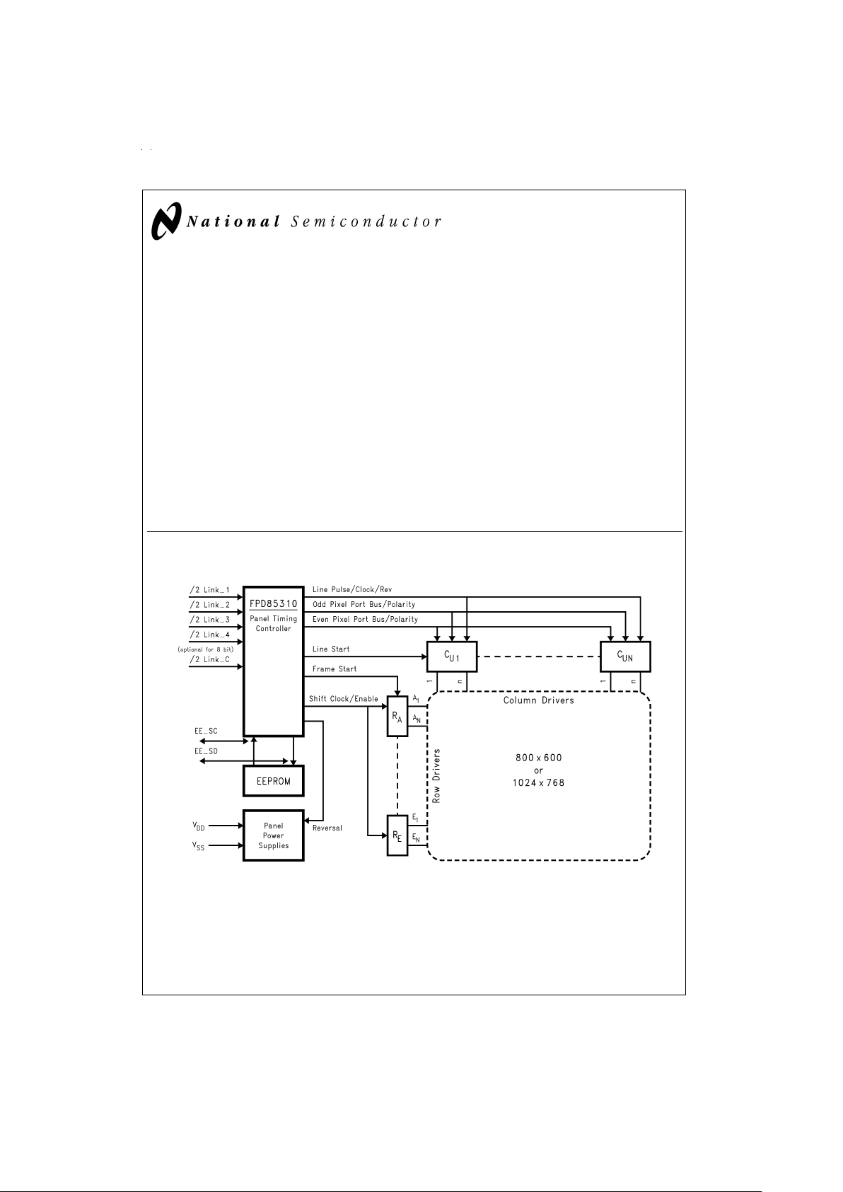
The FPD85310 chip links the panel’s system interface to the
display via a ten wire LVDS data bus. That data is then
routed to the source and gate display drivers. XGA and
SVGA resolutions are supported.
The FPD85310 is programmable via an optional external serial EEPROM. Reserved space in the EEPROM is available
for display identification information. The system can access
the EEPROM to read the display identification data or program initialization values used by the FPD85310.
Features
n FPD-Link System Interface utilizes Low Voltage
Differential Signaling (LVDS).
n System programmable via EEPROM
n Suitable for notebook and monitor applications
n 8-bit or 6-bit system interface
n XGA or SVGA capable
n Supports single or dual port column drivers
n Programmable outputs provide customized control for
standard or in-house column drivers and row drivers
n Fail-safe operation prevents panel damage with system
clock failure
n Programmable skew rate controlled outputs on CD
interface for reduced EMI
n Polarity pin reduces CD data bus switching
n CMOS circuitry operates from a 3.3V supply
System Diagram
TRI-STATE®is a registered trademark of National Semiconductor Corporation.
DS101086-1
September 1999
FPD85310 Panel Timing Controller
© 1999 National Semiconductor Corporation DS101086 www.national.com
Absolute Maximum Ratings (Note 1)
If Military/Aerospace specified devices are required,
please contact the National Semiconductor Sales Office/
Distributors for availability and specifications.
Supply Voltage (V
DD
) 4.1V
DC Input Voltage (V
IN
) −0.5V to VDD+0.5V
DC Output Voltage (V
OUT
) −0.5V to VDD+0.5V
Storage Temperature Range
(T
STG
) −65˚C to +150˚C
Lead Temperature (T
L
)
(Soldering 10 sec.) 260˚C
ESD Rating:
(C
ZAP
= 120 pF, R
ZAP
= 1500Ω)
MM=200V, HBM=2000V
Operating Conditions
Min Max Units
Supply Voltage (V
DD
) 3.0 3.6 V
Operating Temp. Range (T
A
) 0 70 ˚C
Note 1: “Absolute Maximum Ratings” are those values beyond which the
safety of the device cannot be guaranteed. They are not meant to imply that
the devices should be operated at these limits. The table of “Electrical Characteristics” specifies conditions of device operation.
DC Electrical Characteristics T
A
=
0˚C to 70˚C, V
DD
=
3.3V
±
0.3V (unless otherwise specified)
Symbol Parameter Conditions Min Max Units
V
OH
Minimum High Level
Output Voltage
VDD= 3.0V, IOH= 1 mA 2.4 V
V
OL
Maximum Low Level
Output Voltage
VDD= 3.0V, IOL= 1 mA 0.4 V
V
IH
Minimum High Level
Input Voltage
2.0 V
V
IL
Maximum Low Level
Input Voltage
0.8 V
I
IN
Input Current VIN=V
DD
10 µA
I
OZ
Maximum TRI-STATE
Output Leakage Current
VIN=VDD,VIN=V
SS
10 µA
I
DD
Average Supply Current f=65 MHz, C
LOAD
= 50 pF 312 mA
V
THH
Differential Input High
Threshold
Common Mode Voltage = +1.2V +100 mV
V
THL
Differential Input Low
Threshold
Common Mode Voltage = +1.2V -100 mV
Device Specifications T
A
=
0˚C to 70˚C, V
DD
=
3.3V (unless otherwise specified)
Symbol Parameter Conditions Min Max Units
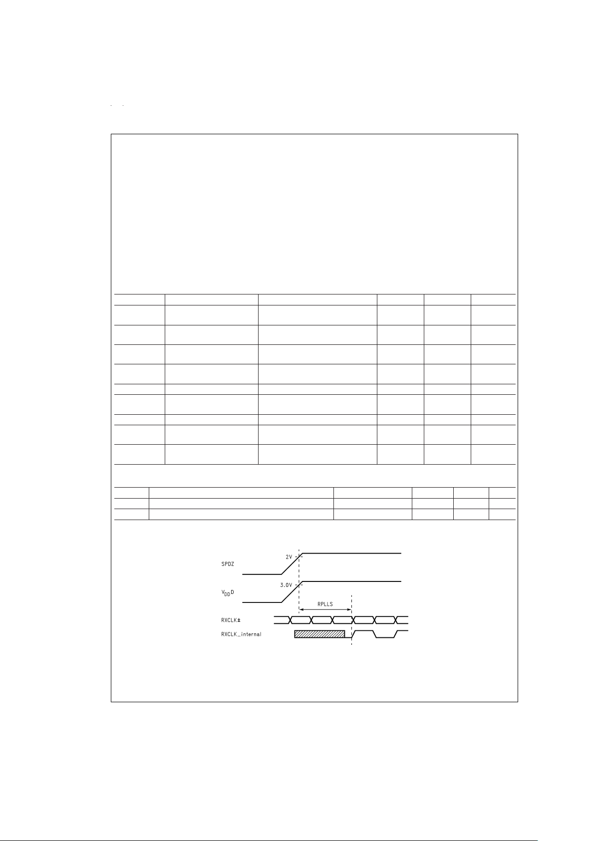
RPLLS Receiver Phase Lock Loop Set Time 10 ms
RCCS RxIN Channel-to-Channel Skew (Note 2) 700 ps
Note 2: This limit assumes a maximum cable skew of 350 ps. Actual automated test equipment limit is 400 ps due to tester accuracy.
DS101086-12
FIGURE 1. FPD85310 (Receiver) Phase Lock Loop Set Time
www.national.com 2
Device Specifications T
A
=
0˚C to 70˚C, V
DD
=
3.3V (unless otherwise specified) (Continued)
Symbol Parameter Conditions Min Max Units
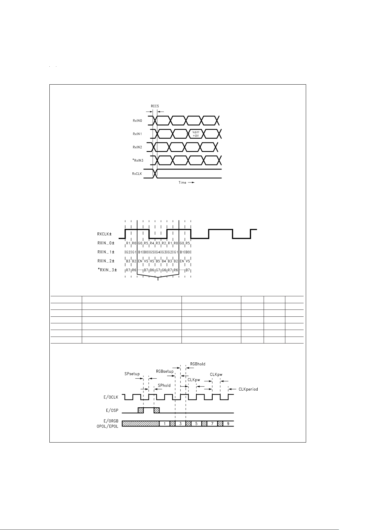
SPsetup E/OSP from E/OCLK 65 MHz Video (Note 6) 8 ns
SPhold E/OSP from E/OCLK 65 MHz Video (Note 6) 8 ns
RGBsetup ER/EG/EB/OR/OG/OB from E/OCLK 65 MHz Video (Note 6) 8 ns
RGBhold ER/EG/EB/OR/OG/OB from E/OCLK 65 MHz Video (Note 6) 8 ns
CLKpw E/OCLK pulsewidth 65 MHz Video (Note 6) 11 ns
CLKperiod E/OCLK period 65 MHz Video (Note 6) 25 ns
Note 6: Timing applies to Dual Bus output modes.
DS101086-13
Note 3: Measurements at V
DIFF
=0V
Note 4: RCCS measured between earliest and latest LVDS edges
Note 5:
*
RxIN3 pair (RxIN_3±) is option for 24-bit color depth
FIGURE 2. FPD85310 (Receiver) Channel-to-Channel Skew and Pulse Width
DS101086-14
FIGURE 3. FPD85310’s (Receiver) Format of the Input Data
DS101086-15
FIGURE 4. Column Driver Bus AC Timing
www.national.com3
Device Specifications T
A
=
0˚C to 70˚C, V
DD
=
3.3V (unless otherwise specified) (Continued)
DS101086-16
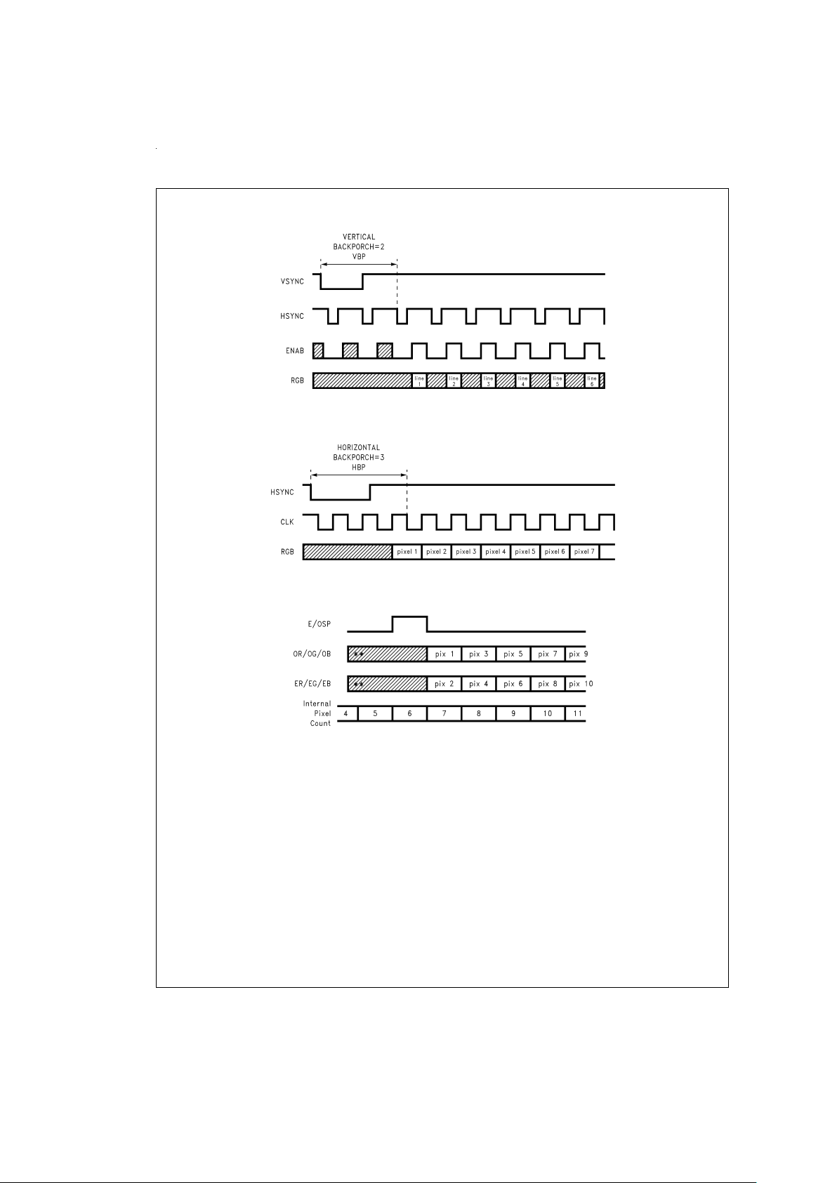
FIGURE 5. Vertical Backporch Definition
(Video Data from Host)
DS101086-17
FIGURE 6. Horizontal Backporch Definition
(Video Data from Host)
DS101086-18
Internal Pixel Count final value = pixels per line/2
Maximum Internal Pixel Count = 1024 (32.5 MHz clocks)
Internal Pixel Count is used to generate the horizontal_component for GPO generation
See
Figure 9
**
Without Blanking control (GPO8), random data may be observed during 16 OCLK and discontinuous 1 OCLK before E/OSP, but it should not be affected to
actual image.
FIGURE 7. Internal Pixel Count Used for GPO Control Generation
www.national.com 4
Device Specifications T
A
=
0˚C to 70˚C, V
DD
=
3.3V (unless otherwise specified) (Continued)
DS101086-19
LC = lines per frame count, LCmax = 2048 lines
Internal Line Count is used to generate the vertical component for GPO generation
See
Figure 9
FIGURE 8. Internal Line Count Used for GPO Control Generation
GPO Generation
DS101086-20
GPO Combination Select
DS101086-21
FIGURE 9. GPO Control Generation
www.national.com5
Device Specifications T
A
=
0˚C to 70˚C, V
DD
=
3.3V (unless otherwise specified) (Continued)
Block Diagram
FPD85310 Default Timing
DS101086-22
Vertical Backporch=35
Lines/Frame=∼825
Pixels/Line=∼1200
Horizontal Backporch=∼100
Displayed pixels/line=1024
(Valid data during ENAB High time)
Displayed lines/frames=768
Frequency=65 MHz (or less)
DS101086-3
www.national.com 6

Functional Description
FPD-LINK RECEIVER
The LVDS based FPD-Link Receiver receives inputs video
data and control timing. Four LVDS channels plus clock provide 24-bit color. Three LVDS channels can be used for
18-bit color.
The video data is regenerated to a parallel data stream and
routed to the 8 to 6 Bit Translator.When SPDZ is active (low)
the FPD85310 is placed in a power down mode. The General Purpose Outputs (GPOs) continue outputting the programmed control sequence at a reduced frame rate. RSTZ
initialized the chip with the default register values. EEPROM
configuration data is loaded if EEPROM is detected. (EEPROM address 80H=“00”).
8 to 6 Bit Translator
8-bit data is reduced to a 6-bit data path via a time multiplexed dithering technique or a simple truncation of the
LSBs. This function is enabled via the Input Control Register
bits 4 and 3. See
Table 2
Input Format Control register.
DATA ALIGNMENT
This function delays and aligns data to match the CD/panel
architect. The following programmable selections in the Output Format Control Register bits 0 and 1 provide support for
various panel architectures. See
Figures 10, 11, 12, 13, 14
for additional explanation.
Dual Bus, Single Port CD Interface
When interfacing two busses to a bank of single port column
drivers, the RGB data must be aligned/delayed with respect
to the size of the column drivers being used. The CD Size
register is programmed to support single port column drivers
of up to 384 outputs (128 pixels).
Dual Bus, Dual Port CD Interface
When interfacing with dual port column drivers, data is simply output with odd and even data on separate outputs.
Single Bus, Single Port CD Interface
The single bus, single port column driver interface provides
support of existing SVGA systems. All data is output on a
single bus. The second bus can be turned off when using
this configuration.
Output Formatting
The output formatting function provides several capabilities
to reduce noise EMI and to generate customized timing.
These capabilities are selectable/programmable via the Output Format Control, Output Enable/Polarity Control, and Output Drive Control Registers. See
Table2
for specific bit defi-
nitions.
Data Bus Skewing
This function aligns the two output channels in either a nonskewed data format (simultaneous switching) or a skewed
data format. The skewed format delays the even channel
data and control by
1
⁄2clock. This reduces the number of out-
puts which switch simultaneously. See
Figures 10, 11, 12,
13, 14
. Data Bus Skewing is enabled by setting bit 2 in the
Output Format Control register.
Programmable Skew Rates
Programmable edge rates allow the Data, Polarity, Start
Pulse, and Clock outputs to be adjusted for better impedance matching for noise and EMI reduction. Bits [7:6] of the
Output Enable/Polarity Control Register control OSP and
ESP outputs. The Output Drive Control register control the
OCLK, ECLK, ORGB/OPOL, ERGB/EPOL outputs.
Polarity Generation
When enabled, a polarity indication is output for each data
bus. If the number of transitions from pixel to pixel exceed 18
bits from 36 bits, the data is inverted and a polarity indication
corresponding to that bus is set active. This requires the use
of a CD with a polarity input and in “SKEWED” mode, OPOL
and EPOL are separated for each skewing then two port CD
need to be two polarity inputs. Polarity Generation is not supported in the single bus/single port CD configuration (SVGA
configuration). The polarity function is enabled by setting bit
6 of the Output Format Control register (EEPROM address
D2). The OCLK and ECLK polarity is also programmable. Inversion and TRI-STATE control of OCLK and ECLK is provided by bits [3:0] of the Output Enable/Polarity Control Register. The ERGB/ESP/EPOL and ORGB/OSP/OPALoutputs
can be disabled (TRI-STATE) using bits [5:4] of the Output
Enable/Polarity Control register.
Programmable Positioning of CD Start Pulse
The position of the CD Start Pulse is programmable. This allows use with column drivers having non-standard start
pulse timing. The CD Start Pulse position is determined by
bits [3:0] of the Output Format Control Register (EEPROM
address D3).
Data Blanking
Data, Polarity,Start Pulse and Clock can be blanked (forced
to “0”) during horizontal and/or vertical blanking periods.
GPO [8] is programmed to correspond to display periods.
When GPO [8] is low, outputs are forced to “0”. This reduces
amount of switching over the frame time thus reducing
power. See GPO programming procedure in
APPENDIX A:
GPO Programming Examples
.
Line Inversion
When enabled (Bit 3 of the Output Format Register), the polarity of the output data is determined by GPO [0]. Bit 4 defines the relationship between GPO [0] and the output data.
Bit 5 provides a variation of this where the Odd and Even
data is of different polarity. This could be used in a system
with CDs on both top and bottom of the panel in which dot inversion is desired.
White Data
The White Data function generates all “1” data beginning at
line 769 and continuing until the beginning of the next frame.
This function is controlled via D6 Register Bit 7.
Timing Control
The Timing Control function generates control to column
drivers, row drivers, and power supply. The programmable
GPOs provide for CD latch pulse, REV,and gate driver control generation. The GPOs allow the user to generate control
anywhere within the frame data. Standard gate driver inter-
www.national.com7

Functional Description (Continued)
face or custom gate interfaces can be implemented with the
nine GPOs. Note that GPO [8] must be used for output
blanking control.
Five registers provide the timing definition for each GPO.
The Horizontal Start register defines the output pixel number
for which the GPO output goes active. The Horizontal duration register determines how many clocks the output will remain active during the line. The VerticalStart register defines
at what line # the output becomes active, and the Vertical duration register defines how many lines the output remains
active. Each output has a control register (bit 0) which defines the GPO polarity (active high or low). Another bit in the
control register (bit 1) enables the “toggle” mode. This mode
is useful in REV generation when alternating polarity is required from line to line. Frame to Frame polarity changes are
made by programming an odd # in the vertical duration register when in “toggle” mode.
Two of the General Purpose Outputs have additional capabilities. GPO [8] controls output blanking and must be used
for this purpose. If output blanking is not desired, this register
must be programmed to always be active. White data generation (all “1” data) at the end of each frame is generated
when D6 register bit 7 is set. When this bit is set, white data
is output after line #768 if GPO [8] is active. GPO [0] is capable of performing line inversion on the output data. Bits
[5:3] of the Output Format Control register provides control
for this function.
See
APPENDIX A: GPO Programming Examples
.
SERIAL EEPROM INTERFACE
The Serial EEPROM Interface controls the FPD85310 initialization. If the EEPROM is not present (EESD and EESC are
pulled high), or if EEPROM address 80H is not “00”, the internal default values are used to initialize all programmable
functions of the FPD85310.
At power-up, the FPD85310 configures the internal programmable registers with data from the EEPROM. After the
FPD85310 is initialized, the EEPROM can be accessed by
the system in which display configuration and manufacturing
information can be obtained. The EEPROM can be programmed “in system” providing quick evaluation of different
display timing.
External access to the EEPROM must be preceded by applying a “1” to pin TEST [2] in order to interrupt the
FPD85310 download.
The FPD85310 initialization data begins at EEPROM address 80H. The first 128 bytes (0-7F) are reserved for display identification data.
A power-up delay can be programmed using bits [6:5] of the
Input Format Control Register. This delays outputting (driving) of the data and control for up to 5 frame times after reset. The TEST [2] pin must be low for a power-up delay to
occur.
VERTICAL/HORIZONTAL REFERENCE GENERATOR
AND FAILURE DETECTION
This block provides Vertical and Horizontal Reference points
for the Timing Control Function. VSYNC, HSYNC and ENAB
along with programmable control from the input control register bits 0 and 1 (FIX HORIZONTAL and FIX VERTICAL)
are used to determine when the video from the host is valid.
Three input modes are supported. See
Table 1
.
Fixed Vertical, Fixed Horizontal
The horizontal timing is fixed and determined by the Horizontal Backporch register. The vertical timing is also fixed and
determined by the Vertical Backporch register. ENAB is ignored and is not necessary.
Fixed Vertical, ENAB Controlled Horizontal
The horizontal timing is controlled by the ENAB timing. The
vertical timing is fixed and determined by the Vertical Backporch register.
ENAB Only
In ENAB Only timing, VSYNC and HSYNC are ignored. All
timing is derived from the ENAB signal.
Failure Detection
The FPD85310 detects the loss of (necessary) control from
the system. VSYNC, HSYNC, ENAB, and CLK are monitored for failure conditions. Failure condition is detected
whenever the input clock stops or when control necessary
for the operational mode is inactive. Failure conditions result
in outputting a default video stream to the panel. Depending
on the mode, loss of CLK, ENAB, HSYNC and/or VSYNC
will result in fail condition output timing. The FPD85310 has
an internal oscillator used for input clock failure detection. If
the input clock quits toggling, the internal oscillator generates the control timing to the column drivers and row drivers.
The internal ring oscillator is disabled when a “1” is applied to
the TEST [3] pin. This will, of course, disable the clock failure
detection capability of the FPD85310. Further description of
the failure detection modes is given in
Table 4
.
www.national.com 8

Functional Description (Continued)
TABLE 1. Input Mode Definition
INPUT FORMAT
FIXED VERTICAL,
FIXED HORIZONTAL
determined by the INPUT
CONTROL REGISTER bits [1:0]
HORIZONTAL
DATA START
VERTICAL
DATA START
FIXED VERTICAL,
FIXED HORIZONTAL
(FIX VERTICAL=1,
FIX HORIZONTAL=1)
Programmable from HSYNC Falling Edge
(# INPUT CLKS)
Programmable from VSYNC
Falling Edge
(# HSYNC PERIODS)
FIXED VERTICAL,
ENAB HORIZONTAL
(FIXED VERTICAL=1,
FIXED HORIZONTAL=0)
Data Valid during ENAB high (HSYNC is
IGNORED)
Programmable from VSYNC
Falling Fdge
(# HSYNC PERIODS)
ENAB ONLY
(FIXED VERTICAL=0,
FIXED HORIZONTAL=0)
Data Valid during ENAB High (HSYNC is
IGNORED)
First ENAB after ENAB low for
greater than one line time (VSYNC
is IGNORED)
Note: INPUT CONTROLREGISTER bit[2] “Enab Detection” provides for “auto-detection” of ENAB. When “1” and Enab is not toggling, the controller will automatically
set the input mode to Fixed Vertical, Fixed Horizontal.
www.national.com9

Functional Description (Continued)
PROGRAMMABLE REGISTERS
At power-up, data is read from an external EEPROM. If anything other than 00H is read back on the first EEPROM access (indicating EEPROM not present), the internal default
values are used. The following parameters are initialized at
power up. Pullups must be used on EE_SD and EE_SC
pins.
TABLE 2. FPD85310 Programmable Register Definition
Control
Registers
EEPROM
Address
The control registers provide mode setting information to the input and output interfaces.
Output Format
Control
D2 [1:0] “00” = Dual Bus, Single port CD interface
“01” = Dual Bus, Dual port CD interface
“10” = Single Bus, Single port CD interface
“11” = Not implemented (defaults to “10”)
[2] “0” = Non-Skewed outputs
“1” = Skewed outputs
[3] “0” = Data inversion is disabled
“1” = Data inversion is enabled
[4] “0” = Data inversion when GPO[0] is “0”
“1” = Data inversion when GPO[0] is “1”
[5] “0” = Even and Odd data inversion when data inversion is enabled
“1” = Odd data inversion determined by bit[4], Even data opposite of Odd data
[6] “0” = Polarity Function disabled
“1” = Polarity Function enabled
[7] “0” = OPOL/EPOL = 0 when data is inverted
“1” = OPOL/EPOL = 1 when data is inverted
D3 [1:0] Odd Start Pulse Offset
“00” = Start pulse 0 clocks before data
“01” = Start pulse 1 clock before data
“10” = Start pulse 2 clocks before data
“11” = Start pulse 3 clocks before data
[3:2] Even Start Pulse Offset
“00” = Start pulse 0 clocks before data
“01” = Start pulse 1 clock before data
“10” = Start pulse 2 clocks before data
“11” = Start pulse 3 clocks before data
[7:4] Unused Pixels
“0000” = no unconnected pixels at beginning of first CD
“0001” = 1 unconnected pixel at beginning of first CD
“0010” = 2 unconnected pixels at beginning of first CD
...
...
“1111” = 15 unconnected pixels at beginning of first CD
www.national.com 10

Functional Description (Continued)
TABLE 2. FPD85310 Programmable Register Definition (Continued)
Control
Registers
EEPROM
Address
The control registers provide mode setting information to the input and output interfaces.
Output
Enable/Polarity
Control
DB [0] OCLK Enable (1-On, 0-TRI-STATE)
[1] OCLK Polarity (1-Per Datasheet, 0-Inverted)
[2] ECLK Enable (1-On, 0-TRI-STATE)
[3] ECLK Polarity (1-Per Datasheet, 0-Inverted)
[4] ORGB/OSP/OPOL Enable (1-On, 0-TRI-STATE)
[5] ERGB/ESP/EPOL Enable (1-On, 0-TRI-STATE)
[7:6] OSP/ESP Control
[7,6] Output
0,0 Lowest Drive
0,1 ..
1,0 ..
1,1 Highest Drive
Output Drive
Control
D4 [1:0] OCLK Control
[3:2] ECLK Control
[5:4] ORGB/OPOL Control
[7:6] ERGB/EPOL Control
[A,B] Output
0,0 Lowest Drive
0,1 ..
1,0 ..
1,1 Highest Drive
CD Size D5 [7:0] = # Data/CD
This number defines how many contiguous pixels are output on the odd and even data
channels for the single port CD interface. CD sizes of up to 128 pixel (384 channel) are
supported. A minimum value of 20H must be programmed regardless of CD interface
used.
Input Format
Control
D6 [0] Fix Vertical
“0” = Vertical position dependent on first ENAB from VSYNC
“1” = Vertical position dependent on Vertical Backporch Register
[1] Fix Horizontal
“0” = Horizontal position dependent on ENAB
“1” = Horizontal position dependent on Horizontal Backporch Register
*See
Table 1
for valid mode combinations.
[2] Enab detection
“0” = Enab detection off
“1” = Enab detection on (detects if Enab is toggling)
Auto Mode switching when Enab detection = “1”
Fix
Vertical
Fix
Horizontal
Enab
Toggling
Operating Mode
0 0 Yes ENAB ONLY
0 0 No FV/FH
1 0 Yes FV/ENAB HORIZ
1 0 No FV/FH
1 1 X FV/FH
Note: Input sync. need to be proceeded before RSTZ goes “high” to determine the “Operating
Mode”
www.national.com11

Functional Description (Continued)
TABLE 2. FPD85310 Programmable Register Definition (Continued)
Control
Registers
EEPROM
Address
The control registers provide mode setting information to the input and output interfaces.
[3] Enable/Disable Virtual 8-bit (8-bit input only)
“0” = Virtual 8-bit enabled
“1” = Virtual 8-bit disabled (Truncate LSBs)
[4] Eight/Six Bit Video
“0” = Six Bit Video
“1” = Eight Bit Video
[6:5] Power-up Delay (TEST2 must be “0”)
“00” = Outputs active after second VSYNC
“01” = Outputs active after third VSYNC
“10” = Outputs active after fourth VSYNC
“11” = Outputs active after fifth VSYNC
[7] White Data Generation
“0”=No white data generation
“1”=Enables white data generation during vertical blanking
Vertical
Backporch (11
bits)
DA, D9 # of HSYNCS from VSYNC falling edge until start of video
Horizontal
Backporch (11
bits)
D8, D7 # of 65 MHz clocks after the falling edge of HSYNC until start of video
General
Purpose Output
Registers
(9 sets)
See
Table 3
EEPROM
Memory
Map
The GPO registers provide complete control over placement of control edges/strobes within the
data frame. The GPO timing registers (Vertical Start, Vertical Duration, Horizontal Start, and
Horizontal Duration) define the control timing relative to the internal line and pixel counters. The
line counter corresponds to the line being displayed. The pixel counter corresponds to the pixel
output each line. The Control Register provides polarity selection and/or generation of a line to
line frame-to-frame alternating signal (REV). Each General Purpose Output can be uniquely
configured. See the GPO programming examples for details.
- GPO [0] provides for the data inversion function enabled by bit 3 of the Output Format Control
Register
- GPO [8] provides programmable data and clock blanking
Vertical Start
(11 bits)
Line # at which GPO [X] control generation begins
Vertical
Duration
(11 bits)
# lines GPO [X] control generation continues
(if “0”, Vertical component is always on)
Horizontal Start
(10 bits)
Internal count (pixel counter) at which GPO [X] goes active to be triggered on rising edge of the
OCLK
Note: If control register [1]=“1”, start position will be moved by 1 pixel clock
Horizontal
Duration
(11 bits)
# Pixel Clocks/2 GPO [X] is active after Horizontal Start
(if “0”, Horizontal component is always on)
www.national.com 12

Functional Description (Continued)
TABLE 2. FPD85310 Programmable Register Definition (Continued)
Control
Registers
EEPROM
Address
The control registers provide mode setting information to the input and output interfaces.
Control Register
(5 bits)
[0]. Output polarity - defines active high or active low output
“0” = normal output (active high)
“1” = inverted output (active low)
[1]. Toggle circuit enable/disable
“0” = Normal GPO output; Toggle circuitry disabled
“1” = Toggle circuitry enabled; output transitions after 1 clock (pixel counter) whenever
programmed rising edge of GPO occurs.
When “toggle circuit” is enable, the value of “Horizontal Duration” register programming
determine; “001h”∼’1 H-line-1’ = 1 H-line toggling, ’1 H-line’∼’2 H-line-1’ = 2 H-line
toggling, etc. up to 11 bits are set.
[2]. Automatic Frame Size Detection
GPO [0:1]
“0” = Normal Operation
“1” = Used with toggle circuitry to create a “continuous” REV signal. NOTE: The value
of the vertical duration register is overwritten.
GPO [2:8]
“0” = Normal Operation
“1” = Early Start capability (Vertical Duration=“00” is N/A, See
Table 5
)
The value in the Vertical Start Register is subtracted from the total number of
lines/frame (auto-detected) to determine the Vertical Start position.
(It needs a full frame after RSTZ, then started with 1 frame delayed to compare to the
other GPOs)
[4:3] GPO [0:8] Combination Select
*
(Two GPOs or multi GPOs)
“00”=Select GPO# as programmed. (no combination function)
“01”=Select GPO# “ANDed” with GPO#-1
“10”=Select GPO# “ORed” with GPO#-1
“11”=Select GPO# and GPO#-1 on alternating frames
(
*
If the transition of GPO#-1 effect the combined result, it should be delayed 1 OCLK,
and GPO0 cannot be programmed by non-existing of “GPO-1”)
(Examples) GPO
#
-1 AND GPO#, (GPO#-2 and GPO#-1) OR GPO#and etc.
TABLE 3. EEPROM Memory Map
Address Data (# bits) Default Values
0-7F DDC VESA DATA (HEX)
80 programmed to 00H for EEPROM auto detect 00
82,81 gpo [8]_pstart_reg (10) 00,01
84,83 gpo [8]_pcount_reg (11) 02,2D
86,85 gpo [8]_lstart_reg (11) 00,01
88,87 gpo [8]_lcount_reg (11) 03,02
89 gpo [8]_cont_reg (5) 00
8B,8A gpo [7]_pstart_reg (10) 00,14
8D,8C gpo [7]_pcount_reg (11) 01,E0
8F,8E gpo [7]_lstart_reg (11) 00,02
91,90 gpo [7]_lcount_reg (11) 03,00
92 gpo [7]_cont_reg (5) 01
www.national.com13
Functional Description (Continued)
TABLE 3. EEPROM Memory Map (Continued)
Address Data (# bits) Default Values
94,93 gpo [6]_pstart_reg (10) 00,01
96,95 gpo [6]_pcount_reg (11) 02,9F
98,97 gpo [6]_lstart_reg (11) 01,FD
9A,99 gpo [6]_lcount_reg (11) 00,01
9B gpo [6]_cont_reg (5) 01
9D,9C gpo [5]_pstart_reg (10) 00,01
9F,9E gpo [5]_pcount_reg (11) 02,9F
A1,A0 gpo [5]_lstart_reg (11) 00,FD
A3,A2 gpo [5]_lcount_reg (11) 00,01
A4 gpo [5]_cont_reg (5) 01
A6,A5 gpo [4]_pstart_reg (10) 00,01
A8,A7 gpo [4]_pcount_reg (11) 02,9F
AA,A9 gpo [4]_lstart_reg (11) 03,22
AC,AB gpo [4]_lcount__reg (11) 00,01
AD gpo [4]_cont_reg (5) 01
AF,AE gpo [3]_pstart_reg (10) 01,E0
B1,B0 gpo [3]_pcount_reg (11) 00,28
B3,B2 gpo [3]_lstart_reg (11) 00,01
B5,B4 gpo [3]_lcount_reg (11) 00,00
B6 gpo [3]_cont_reg (5) 01
B8,B7 gpo [2]_pstart_reg (10) 02,0B
BA,B9 gpo [2]_pcount_reg (11) 00,14
BC,BB gpo [2]_lstart_reg (11) 00,01
BE,BD gpo [2]_lcount_reg (11) 03,00
BF gpo [2]_cont_reg (5) 00
C1,C0 gpo [1]_pstart_reg (10) 02,0D
C3,C2 gpo [1]_pcount_reg (11) 00,0A
C5,C4 gpo [1]_lstart_reg (11) 00,01
C7,C6 gpo [1]_lcount_reg (11) 03,01
C8 gpo [1]_cont_reg (5) 03
CA,C9 gpo [0]_pstart_reg (10) 02,0D
CC,CB gpo [0]_pcount_reg (11) 00,0A
CE,CD gpo [0]_lstart_reg (11) 00,01
D0,CF gpo [0]_lcount_reg (11) 03,01
D1 gpo [0]_cont_reg (5) 02
D3,D2 output_format (16) 00,00
D4 output_drive (8) AA
D5 cd_size (8) 67
D6 input_format (8) 01
www.national.com 14

Functional Description (Continued)
TABLE 3. EEPROM Memory Map (Continued)
Address Data (# bits) Default Values
D8,D7 hbp_reg (11) 00,94
DA,D9 vbp_reg (11) 00,23
DB output_enable/polarity_control (8) BF
FF–DC not used/not loaded —
DS101086-4
Note 7: Programmable CD Size “n” (up to 128)
Note 8: One or both clocks can be used
Note 9: Unused clocks can be turned off
Note 10: E/OCLK polarity is programmable
FIGURE 10. Dual Bus Single Port Column Driver Interface
(Non-skewed outputs)
www.national.com15

Functional Description (Continued)
DS101086-5
Note 11: Programmable CD Size “n” (up to 128)
Note 12: Data skewed to reduce simultaneous switching
FIGURE 11. Dual Bus Single Port Column Driver Interface
(Skewed outputs)
www.national.com 16

Functional Description (Continued)
DS101086-6
Note 13: One or both clocks can be used
Note 14: Unused clock can be turned off
FIGURE 12. Dual Bus Dual Port Column Driver Interface
(Non-skewed outputs)
www.national.com17

Functional Description (Continued)
DS101086-7
Note 15: Data skewed to reduce simultaneous switching
FIGURE 13. Dual Bus Dual Port Column Driver Interface
(Skewed outputs)
www.national.com 18

Functional Description (Continued)
DS101086-8
Note 16: ECLK/ERGB not used— These outputs can be disabled by setting bits 2 and 5 to “0” in the Output Enable/Polarity Control register.
Note 17: Start pulse offset
*
(D3 [1:0]) is defined as below only in this mode.
“00”— Start pulse 1 clock after 1st data
“01”— Start pulse 1 clock before 1st data
“10”— Start pulse 3 clocks before 1st data
“11”—Start pulse 5 clocks before 1st data
*
Start pulse position can be adjusted precisely by unused pixels register (D3 [7:4])
Note 18: The Pcount and Pstart registers are programmed by 2 OCLK only in this mode. (Example) Pcount Register=“02”:4 OCLK duration
FIGURE 14. Single Port Single Bus Column Driver Interface
(SVGA Application)
DS101086-9
Note 19: Total of eight GPOs for REV, LP, and Gate Driver Control (GPO [8] dedicated to blanking function)
Note 20: GPO resolution is video clock/2
FIGURE 15. Standard or Custom Gate Driver Interface
www.national.com19

Functional Description (Continued)
DS101086-10
Note 21: RSTZ transition Low-to-High occurs at the completion of the RPLLS delay or later as shown above.
Note 22: All outputs* forced low in default timing of FPD85310 during power-up delay time.
Note 23: All outputs
**
forced low in continuous download (every two frame) mode.
Note 24: All outputs
***
generate the signal for default values in FPD85310 and unknown values when use the EEPROM values during power-up delay time. Then
NS recommend to use the continuous download mode.
Note 25: EEPROM download occurs at first detected vertical blanking period.
Note 26: Active outputs depends on INPUT FORMAT register bits [5:6].
INPUT
FORMAT
[5:6]
VSYNC# at which
outputs go active
00 Second VSYNC
01 Third VSYNC
10 Fourth VSYNC
11 Fifth VSYNC
Note 27: When configured in ENAB Only Mode (EOM), VSYNC signals are unused except for timing EEPROM DownLoad Sequences. When configured with default values in Fixed Vertical mode, the VSYNC signal is generated any time ENAB remains low for more than 2 horizontal periods.
During Power Up, before Reset has propagated, the EEPROM may receive spurious addressing that initiates a down load sequence, but the output data is often
not captured for lack of timing alignment with VSYNC. In the case where EEPROM data is not captured during the initial (automatic) Reset or Power Up DownLoad
sequence, Timing Controller outputs are indeterminate until the EEPROM data is successfully loaded, which always begins and is executed at the next VSYNC valid
(low) cycle.
Note 28: During Power Up sequences, false RSTZ signals are possible due to instability of the power supply level, typically within the 10 ms of operation. Toavoid
this situation, implementation of the circuit in
Figure 17
, or other functional equivalent, is recommended, (
Figure 17
).
FIGURE 16. Power-up Sequence (INPUT FORMAT[6:5] = “01”)
www.national.com 20

Functional Description (Continued)
FAILURE DETECTION
TABLE 4. FPD85310 Failure Detection
Mode
No
Clock
No
VSYNC
No
HSYNC
No
ENAB
Fix Vertical/Horizontal (1) (2) (3) —
Fix Vertical/ENAB Horizontal (1) (2) — (4)
ENAB Only Mode (1) — — (5)
(1) Wait (∼2) ms then output 2048 pixels/line and 2047 lines/frame. No esp/osp. No eclk/oclk.
(2) Wait (∼2) ms then output input line time and 2047 lines/frame. With esp/osp. With eclk/oclk.
(3) Wait (∼2) ms then output 2048 pixels/line and input frame time. With esp/osp. With eclk/oclk.
(4) Wait (∼2) ms then output 2048 pixels/line and input frame time. No esp/osp. With eclk/oclk.
(5) Wait (∼2) ms then output 2048 pixels/line and 2047 lines/frames. No esp/osp. With eclk/oclk.
*default frame size is 2048 lines x 2048 pixels
@
pixel rate of ∼25 MHz.
*GPO control outputs are generated per programmed values.
DS101086-11
FIGURE 17. Delay Circuit for Stable RSTZ
www.national.com21

Connection Diagram
Pin Description
Pin No:
Pin Count
Pin Name I/O Description
SYSTEM INTERFACE
2 RXIN_0
±
LVDI FPD-Link data pair 0
2 RXIN_1
±
LVDI FPD-Link data pair 1
2 RXIN_2
±
LVDI FPD-Link data pair 2
2 RXIN_3
±
LVDI FPD-Link data pair 3
(used in 8-bit video applications)
2 RXCLK
±
LVDI FPD-Link Clock
1 RSTZ I Reset, Active Low
1 SPDZ I System Power Down control input. Active Low;
FPD-Link output are low, then FPD85310 goes to
Failure detection mode.
DS101086-2
Order Number FPD85310VJD
See NS Package Number VJD100A
www.national.com 22

Pin Description (Continued)
Pin No:
Pin Count
Pin Name I/O Description
COLUMN DRIVER INTERFACE
1 ECLK POH Even CD Bus Clock
1 ESP POL Even Start Pulse
6 ER0..ER5 POL Even Red Bus:
6 EG0..EG5 POL Even Green Bus:
6 EB0..EB5 POL Even Blue Bus:
1 EPOL POL Even Polarity
1 OCLK POH Odd CD Bus Clock
1 OSP POL Odd Start Pulse
6 OR0..OR5 POL Odd Red Bus:
6 OG0..OG5 POL Odd Green Bus:
6 OB0..OB5 POL Odd Blue Bus:
1 OPOL POL Odd Polarity
GENERAL PURPOSE OUTPUTS
9 GPO[8:0] TO General Purpose Outputs
EEPROM INTERFACE
1 EE_SD I/TO EEPROM Serial Data
1 EE_SC I/TO EEPROM Clock
POWER SUPPLY
1V
DD
A P PLL and Bandgap Supply
1 GND1 G PLL Ground
1 GNDA G Bandgap Ground
1V
DD
D P LVDS Receiver Supply
1 GNDD G LVDS Receiver Ground
10 V
SS
IO G IO Ground
9V
DD
IO P IO Power
3V
SS
G Digital Ground
3V
DD
P Digital Power
TEST/CONFIGURATION
5 TEST[4–0] I Test/Configuration Pins.
TEST[0]—Must be “0”
TEST[1]—Must be “0”
TEST[2]
“0” — EEPROM init values loaded every 2
frames
“1” — EEPROM init values loaded once at
power-up
TEST[3]
“0” — Ring Oscillator Enable
“1” — Ring Oscillator Disable
TEST[4]—Must be “0”
•
I/TO — TTL Input/TRI-STATE®output
•
TO — TRI-STATE output
•
POL — Programmable (Low Drive)
•
POH — Programmable (High Drive)
•
I — TTL Input
•
LVDI — Low Voltage Differential Input
•
P — Power
•
G — Ground
www.national.com23

APPENDIX A: GPO Programming
Examples
The GPO control generation is based on the internal line
count and pixel count shown in
Figure 7
and
Figure 8
.Two
programmable registers (Vertical Start and VerticalDuration)
control the vertical component of the control signal. This establishes at what line and for how many lines the control signal will be active. Likewise, two programmable registers
(Horizontal Start and Horizontal Duration) control the horizontal component of the control signal. The Horizontal register values determine at what pixel count the signal goes active and for how many pixel counts the signal stays active
during each line. The Vertical Component enables the signal
for however many lines programmed for and the Horizontal
Component generates pulses within that vertical time period.
Generally the following types of signals are generated:
1. DC (either 1 or 0)
2. A pulse every line
3. A pulse once a frame (either in pixels or lines)
4. Pulsed during active video (pulses are blanked during
vertical blanking period of frame)
Table5
describes the programming requirements for general
types of pulses generated.
The GPO’s also have a “toggle mode”. This provides the ca-
pability to generate a “REVERSAL” signal used in most LCD
applications. Bit 1 of the Control register is set toa1toenable toggle mode operation. The GPO is programmed so
that a rising edge is produced when the control signal is required to toggle. This generally occurs once each line. Also,
the # of edges generated per frame is programmed to be an
odd #. This ensures that the control signal will alternate polarity from frame to frame.
Examples of GPO programming to produce specific control
signals are included in the following pages.
TABLE 5. GPO Pulse Generation
Vertical
Start
Vertical
Duration
Horizontal
Start
Horizontal
Duration
GPO Output
=
don’t care =0 =0 =0 Stuck 0 (When Output Polarity = 0)
Stuck 1 (When Output Polarity = 1)
Polarity control is in GPO Control Register bit 0
=
don’t care =0
#
A =0 Stuck 1 (When Output Polarity = 0)
Stuck 0 (When Output Polarity = 1)
Polarity control is in GPO Control Register bit 0
=don’t care =0 #A #B
(Note 29)
Pulse is generated every line beginning at ∼#A
32 MHz clocks from start of output line and lasting for
#B 32 MHz clocks
#A #B #C =0 Pulse begins at line #A , clock #C and continues to
line #(A+B) pixel #C (multi-line pulse)
#A #B #C #D
(Note 29)
Pulse generation begins at line A and continues for #B
lines. Each pulse begins at ∼pixel #C and lasts for D
counts
Note 29: Pulses will occur every other line if Horizontal Duration is greater than a line time.
www.national.com 24

APPENDIX A: GPO Programming Examples (Continued)
GPO Programming Example #1:
Generate a control signal which transitions high at the end of
each line, has a pulsewidth of 3 µs, and remains low during
the vertical blanking period. This control is used for the latch
pulse to the column drivers.
Horizontal time (clocks/line) = 1300 dot clocks
Vertical period (lines/frame) = 850 lines
Vertical control is active beginning at line 1 and remains active for 768 lines.
GPO Vertical Start Register = 1
GPO Vertical Duration Register = 768d (300h)
Positive pulse goes high each line at output clock 512 corresponding to when the last two pixels are output on OR, OG,
OB, ER, EG, EB. Pulse remains high for 98 output clocks (98
x 30.8 ns/clock = 3.02 µs). (Dual Bus output clock =
32.5 MHz for 65 MHz XGA video, 1024 pixels/line, 768 displayed lines/frame).
Note: 6 counts are added to the output start # because the GPO pixel count
begins 6 clocks prior to the output data.
GPO Horizontal Start Register = 518d (206h)
GPO Horizontal Duration Register = 98d (62h)
The control pulses are positive (bit [0] = 0) and the toggle circuitry is disabled (bit1 [1] = 0).
GPO Control Register = 0
DS101086-23
www.national.com25

APPENDIX A: GPO Programming
Examples
(Continued)
GPO Programming Example #2:
Generate a control signal which transitions low 20 output
clocks after the beginning of each output line, has a pulsewidth (low) of 12 µs, and goes high during horizontal blanking. This control signal is used as an output enable for the
gate drivers.
Horizontal time (clocks/line) = 1300 dot clocks
Vertical period (lines/frame) = 850 lines
Control is active beginning at line 2 and remains active for
768 lines.
GPO Vertical Start Register = 2
GPO Vertical Duration Register = 768d (300h)
Negative pulse goes low each line at output clock 20 corresponding to when the 39/40 pixels are output on OR, OG,
OB, ER, EG, EB. Pulse remains low for 390 output clocks
(390 x 30.8 ns/clock = 12 µs). (Dual Bus output clock =
32.5 MHz for 65 MHz XGA video, 1024 pixels/line, 768 lines/
frame).
Note: 6 counts are added to the output clock # because the GPO start count
begins 6 clocks prior to the output data.
GPO Horizontal Start Register = 26d (1ah)
GPO Horizontal Duration Register = 390d (186h)
The control pulses are negative (bit [0] = 1) and the toggle
circuitry is disabled (bit1 [1] = 0).
GPO Control Register = 1
DS101086-24
www.national.com 26

APPENDIX A: GPO Programming
Examples
(Continued)
GPO Programming Example #3:
Generate a control signal which toggles during horizontal
blanking and alternates polarity each frame. This control signal is used as the reversal signal.
Horizontal time (clocks/line) = 1300 dot clocks
Vertical period (lines/frame) = 850 lines
Control is active beginning at line 1 and remains active for
769 lines.
(Odd number programmed in Duration Register causes control signal to alternate polarity each frame)
GPO Vertical Start Register = 1
GPO Vertical Duration Register = 769d (301h)
Positive going pulse causes output to toggle. Edge occurs
20 output clocks after end of each line (1024/2 + 20 = 532).
Pulse duration is not critical since the output will be in toggle
mode. (Dual Bus output clock = 32.5 MHz for 65 MHz XGA
video, 1024 pixels/line, 768 lines/frame).
Note: 6 counts are added to the output start # because the GPO pixel count
begins 6 clocks prior to the output data.
GPO Horizontal Start Register = 538 (238h)
GPO Horizontal Duration Register = 10d (0Ah)
The control pulses are positive (bit [0] = 0) and the toggle circuitry is enabled (bit1 [1] = 1).
GPO Control Register = 2
(For a second control signal of opposite polarity, program another GPO Control Register with same count values with
GPO Control Register = 3.)
DS101086-25
www.national.com27

APPENDIX B:
National Semiconductor
FPD85310 REQUEST FORM OF MASK VERSION
Company Name:_________________________________Dept:______________________ Tel: _____________________
Model Name (Application): ______________________________________________
Register Values:
TABLE 6. Register Values for GPO[0:8]’s Programming
Pin
Name
Address/Values (Hex.)
Name of Signal
for USER
Remarks
GPO8
Address 81 82 83 84 85 86 87 88 89
Value
GPO7
Address 8A 8B 8C 8D 8E 8F 90 91 92
Value
GPO6
Address 93 94 95 96 97 98 99 9A 9B
Value
GPO5
Address 9C 9D 9E 9F A0 A1 A2 A3 A4
Value
GPO4
Address A5 A6 A7 A8 A9 AA AB AC AD
Value
GPO3
Address AE AF B0 B1 B2 B3 B4 B5 B6
Value
GPO2
Address B7 B8 B9 BA BB BC BD BE BF
Value
GPO1
Address C0 C1 C2 C3 C4 C5 C6 C7 C8
Value
GPO0
Address C9 CA CB CC CD CE CF D0 D1
Value
TABLE 7. Register Values for LCD Format Control
Control Register Address/Values (Hex.) Control Register Address/Values (Hex.) Remarks
Output_Format
Address D2 D3
Output_Drive
Address D4
Value Value
C/D_Size
Address D5
Input_Format
Address D6
Value Value
HBP_REG
Address D7 D8
VBP_REG
Address D9 DA
Value Value
Output_Enable/
Polarity_Control
Address DB
Value
Signature by Customer _____________________________Date _____________
www.national.com 28

Physical Dimensions inches (millimeters) unless otherwise noted
LIFE SUPPORT POLICY
NATIONAL’S PRODUCTS ARE NOT AUTHORIZED FOR USE AS CRITICAL COMPONENTS IN LIFE SUPPORT
DEVICES OR SYSTEMS WITHOUT THE EXPRESS WRITTEN APPROVAL OF THE PRESIDENT AND GENERAL
COUNSEL OF NATIONAL SEMICONDUCTOR CORPORATION. As used herein:
1. Life support devices or systems are devices or
systems which, (a) are intended for surgical implant
into the body, or (b) support or sustain life, and
whose failure to perform when properly used in
accordance with instructions for use provided in the
labeling, can be reasonably expected to result in a
significant injury to the user.
2. A critical component is any component of a life
support device or system whose failure to perform
can be reasonably expected to cause the failure of
the life support device or system, or to affect its
safety or effectiveness.
National Semiconductor
Corporation
Americas
Tel: 1-800-272-9959
Fax: 1-800-737-7018
Email: support@nsc.com
National Semiconductor
Europe
Fax: +49 (0) 1 80-530 85 86
Email: europe.support@nsc.com
Deutsch Tel: +49 (0) 1 80-530 85 85
English Tel: +49 (0) 1 80-532 78 32
Français Tel: +49 (0) 1 80-532 93 58
Italiano Tel: +49 (0) 1 80-534 16 80
National Semiconductor
Asia Pacific Customer
Response Group
Tel: 65-2544466
Fax: 65-2504466
Email: sea.support@nsc.com
National Semiconductor
Japan Ltd.
Tel: 81-3-5639-7560
Fax: 81-3-5639-7507
www.national.com
Plastic Quad Flatpak, JEDEC
NS Package Number VJD100A
FPD85310 Panel Timing Controller
National does not assume any responsibility for use of any circuitry described, no circuit patent licenses are implied and National reserves the right at any time without notice to change said circuitry and specifications.
 Loading...