NSC DSV14196WMX, DSV14196TWMX, DSV14196TWM Datasheet

DSV14196
+3.3V Supply EIA/TIA-232 5 Driver x 3 Receiver
General Description
The DSV14196/DSV14196T is a five driver, three receiver
device which conforms to the EIA/TIA-232-E and the ITU-T
V.28 standards.
The flow-through pinout facilitates simple non-crossover
board layout. The DSV14196/DSV14196T provides a peripheral side one-chip solution for the common 9-pin serial
RS-232 interface between data terminals and data communications equipment.
Features
n Conforms to EIA/TIA-232-E and ITU-T V.28
n 5 drivers and 3 receivers
n Flow-through pinout
n Failsafe receiver outputs high when inputs open
n 20-pin wide SOIC package
n LapLink
®
compatible—230.4 kbps data rate
n +3.3V Logic Interface
n Commercial temperature range option DSV14196
(0˚C to 70˚C)
n Industrial temperature range option DSV14196T
(−40˚C to +85˚C)
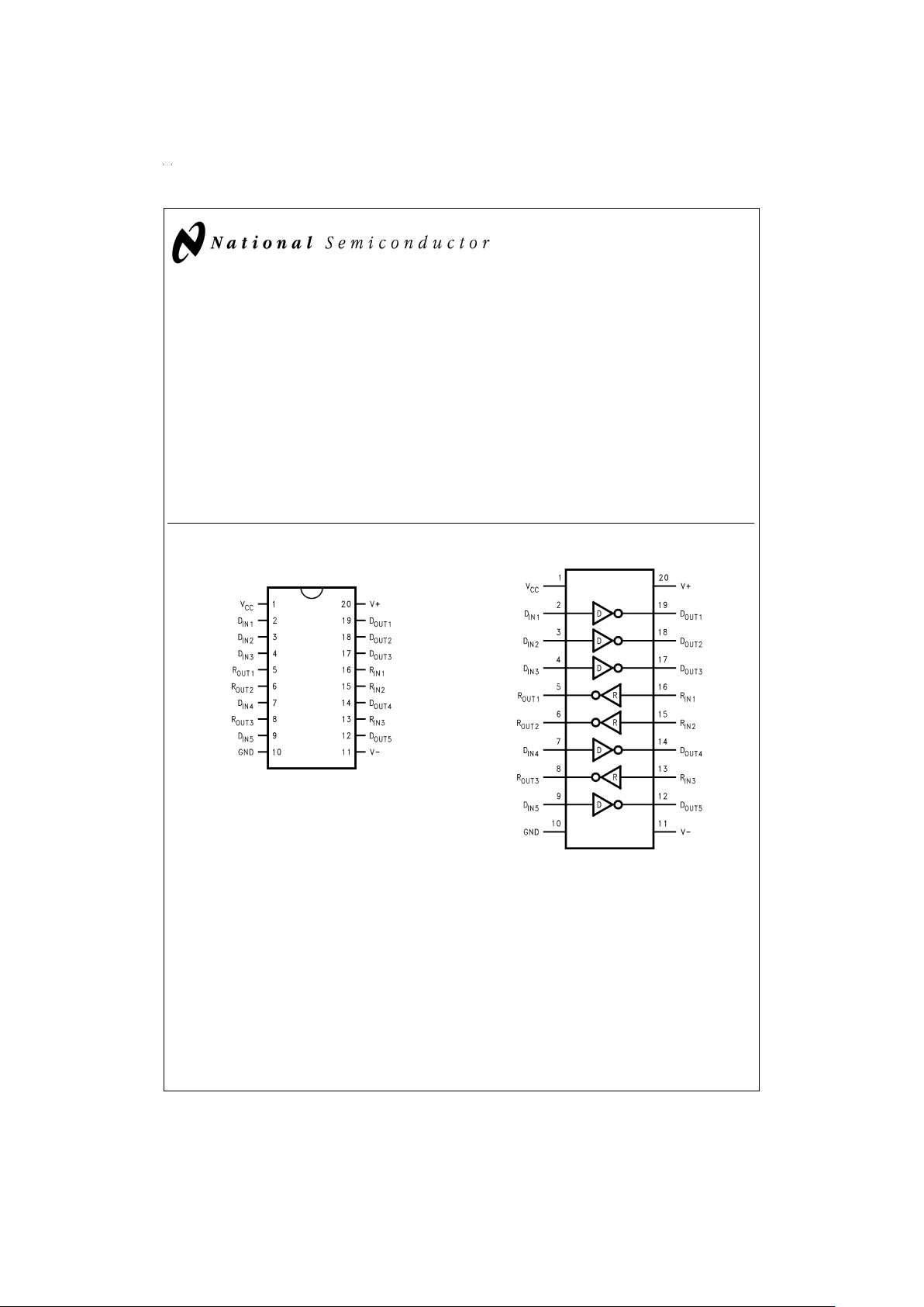
Connection Diagram Functional Diagram
LapLink®is a registered trademark of Travelling Software.
SOP
DS100853-1
Order Number DSV14196WM,DSV14196TWM
See NS Package Number M20B
DS100853-2
April 1999
DSV14196+3.3V Supply EIA/TIA-232 5 Driver x 3 Receiver
© 1999 National Semiconductor Corporation DS100853 www.national.com

Absolute Maximum Ratings (Note 1)
If Military/Aerospace specified devices are required,
please contact the National Semiconductor Sales Office/
Distributors for availability and specifications.
Supply Voltage (V
CC
) +7V
Supply Voltage (V
+
) +15V
Supply Voltage (V
−
) −15V
Driver Input Voltage 0V to V
CC
Driver Output Voltage (Power Off)
±
15V
Receiver Input Voltage
±
25V
Receiver Output Voltage (R
OUT
) 0VtoV
CC
Maximum Power Package Dissipation@+25˚C
M Package 1524 mW
Derate M Package 12.2 mW/˚C above 25˚C
Storage Temperature Range −65˚C to +150˚C
Lead Temperature Range (Soldering, 4 sec.) +260˚C
ESD Ratings (HBM. 1.5 kΩ, 100 pF) ≥1.5 kV
Recommended Operating
Conditons
Min Nom Max Units
Supply Voltage (V
CC
) +3.0 +3.3 +3.6 V
Supply Voltage (V
+
) +9.0 +12.0 +13.2 V
Supply Voltage (V
−
) −13.2 −12.0 −9.0 V
Operating Free Air
Temperature (T
A
)
DSV14196 0 +25 +70 ˚C
DSV14196T −40 +25 +85 ˚C
Electrical Characteristics(Note 2) (Note 3)
DSV14196
Over recommended operating supply and temperature ranges unless otherwise specified
Symbol Parameter Conditions Min Typ Max Units
DEVICE CHARACTERISTICS
I
CC
VCCSupply Current No Load, All Inputs at +3.3V 8 16 mA
I
+
V+Supply Current No Load, All
Driver Inputs at
0.8V or +2V. All
Receiver Inputs
at 0.7V or 2.4V.
V
+
=
+9V, V
−
=
−9V 16 26 mA
V
+
=
+13.2V, V
−
=
−13.2V 23 36 mA
I
−
V−Supply Current V
+
=
+9V, V
−
=
−9V −18 −26 mA
V
+
=
+13.2V, V
−
=
−13.2V −25 −36 mA
DRIVER CHARACTERISTICS
V
IH
High Level Input Voltage 2.0 V
V
IL
Low Level Input Voltage 0.8 V
I
IH
High Level Input Current V
IN
=
3.3V 10 µA
I
IL
Low Level Input Current V
IN
=
0V −1.1 −1.5 mA
V
OH
High Level Output Voltage R
L
=
3kΩ,V
IN
=
0.8V, V
+
=
+9V, V
−
=
−9V 6 7 V
R
L
=
3kΩ,V
IN
=
0.8V, V
+
=
+12V, V
−
=
−12V 8 9 V
R
L
=
7kΩ,V
IN
=
0.8V, V
+
=
+13.2V, V
−
=
−13.2V 10 11.5 V
V
OL
Low Level Output Voltage R
L
=
3kΩ,V
IN
=
2V, V
+
=
+9V, V
−
=
−9V −7 −6 V
R
L
=
3kΩ,V
IN
=
2V, V
+
=
+12V, V
−
=
−12V −10 −8 V
R
L
=
7kΩ,V
IN
=
2V, V
+
=
+13.2V, V
−
=
−13.2V −11.5 −10 V
I
OS
+ Output High Short V
OUT
=
0V, V
IN
=
0.8V −6 −12 −18 mA
Circuit Current (Note 4)
I
OS
− Output Low Short V
OUT
=
0V, V
IN
=
2.0V 6 12 18 mA
Circuit Current (Note 4)
R
O
Output Resistance −2V ≤ V
OUT
≤ +2V, V
+
=
V
−
=
V
CC
=
0V 300 Ω
−2V ≤ V
OUT
≤ +2V, V
+
=
V
−
=
V
CC
=
Open Circuit 300 Ω
www.national.com 2

Electrical Characteristics(Note 2) (Note 3)
DSV14196 (Continued)
Over recommended operating supply and temperature ranges unless otherwise specified
Symbol Parameter Conditions Min Typ Max Units
RECEIVER CHARACTERISTICS
V
TH
Input High Threshold V
OUT
≤ 0.4V, I
O
=
3.2 mA 1.5 1.85 2.4 V
(Recognized as a High
Signal)
V
TL
Input Low Threshold
(Recognized as a Low
Signal)
V
OUT
≥ 1.7V, I
O
=
−0.5 mA 0.7 0.9 1.3 V
R
IN
Input Resistance V
IN
=
±
3V to±15V 3.0 3.8 7.0 kΩ
I
IN
Input Current V
IN
=
+15V 2.1 4.0 5.0 mA
V
IN
=
+3V 0.43 0.7 1.0 mA
V
IN
=
−15V −2.1 −4.0 −5.0 mA
V
IN
=
−3V −0.43 −0.7 −1.0 mA
V
OH
High Level Output Voltage
(Note 7)
I
OH
=
−0.5 mA, V
IN
=
−3V 1.7 2.4 V
I
OH
=
−10 µA, V
IN
=
−3V 2.7 3.2 V
I
OH
=
−0.5 mA, V
IN
=
Open Circuit 1.7 2.4 V
I
OH
=
−10 µA, V
IN
=
Open Circuit 2.7 3.2 V
V
OL
Low Level Output Voltage I
OL
=
3.2 mA, V
IN
=
+3V 0.2 0.4 V
I
OSR
Short Circuit Current V
OUT
=
0V, V
IN
=
0V (Note 4) −0.6 −1.8 −3.0 mA
Electrical Characteristics(Note 2) (Note 3)
DSV14196T
Over recommended operating supply and temperature ranges unless otherwise specified
Symbol Parameter Conditions Min Typ Max Units
DEVICE CHARACTERISTICS
I
CC
VCCSupply Current No Load, All Inputs at +3.3V 8 16 mA
I
+
V+Supply Current No Load, All
Driver Inputs at
0.8V or +2V. All
Receiver Inputs
at 0.7V or 2.4V.
V
+
=
+9V, V
−
=
−9V 16 26 mA
V
+
=
+13.2V, V
−
=
−13.2V 23 36 mA
I
−
V−Supply Current V
+
=
+9V, V
−
=
−9V −18 −26 mA
V
+
=
+13.2V, V
−
=
−13.2V −25 −36 mA
DRIVER CHARACTERISTICS
V
IH
High Level Input Voltage 2.0 V
V
IL
Low Level Input Voltage 0.8 V
I
IH
High Level Input Current V
IN
=
3.3V 10 µA
I
IL
Low Level Input Current V
IN
=
0V −1.1 −1.9 mA
V
OH
High Level Output Voltage R
L
=
3kΩ,V
IN
=
0.8V, V
+
=
+9V, V
−
=
−9V 5.5 7 V
R
L
=
3kΩ,V
IN
=
0.8V, V
+
=
+12V, V
−
=
−12V 7.5 9 V
R
L
=
7kΩ,V
IN
=
0.8V, V
+
=
+13.2V, V
−
=
−13.2V 9 11.5 V
V
OL
Low Level Output Voltage R
L
=
3kΩ,V
IN
=
2V, V
+
=
+9V, V
−
=
−9V −7 −5.5 V
R
L
=
3kΩ,V
IN
=
2V, V
+
=
+12V, V
−
=
−12V −10 −7.5 V
R
L
=
7kΩ,V
IN
=
2V, V
+
=
+13.2V, V
−
=
−13.2V −11.5 −9 V
I
OS
+ Output High Short V
OUT
=
0V, V
IN
=
0.8V −4 −12 −22 mA
Circuit Current (Note 4)
I
OS
− Output Low Short V
OUT
=
0V, V
IN
=
2.0V 4 12 22 mA
Circuit Current (Note 4)
R
O
Output Resistance −2V ≤ V
OUT
≤ +2V, V
+
=
V
−
=
V
CC
=
0V 300 Ω
−2V ≤ V
OUT
≤ +2V, V
+
=
V
−
=
V
CC
=
Open Circuit 300 Ω
www.national.com3
 Loading...