

DS96F173M/DS96F175C/DS96F175M
EIA-485/EIA-422 Quad Differential Receivers
General Description
The DS96F173 and the DS96F175 are high speed quad differential line receivers designed to meet the EIA-485 standard. The DS96F173and the DS96F175 offer improved performance due to the use of L-FAST bipolar technology. The
use of LFAST technology allows the DS96F173 and
DS96F175 to operate at higher speeds while minimizing
power consumption.
The DS96F173 and the DS96F175 have TRI-STATE
®
outputs and are optimized for balanced multipoint data bus
transmission at rates up to 15 Mbps. The receivers feature
high input impedance, input hysteresis for increased noise
immunity, and input sensitivity of 200 mV over a common
mode input voltage range of −7V to +12V.The receivers are
therefore suitable for multipoint applications in noisy environments. The DS96F173 features an active high and active
low Enable, common to all four receivers. The DS96F175
features separate active high Enables for each receiver pair.
Features
n Meets EIA-485, EIA-422A, EIA-423A standards
n Designed for multipoint bus applications
n TRI-STATE outputs
n Common mode input voltage range: −7V to +12V
n Operates from single +5.0V supply
n Reduced power consumption (I
CC
= 50 mA max)
n Input sensitivity of
±
200 mV over common mode range
n Input hysteresis of 50 mV typical
n High input impedance
n Military temperature range available
n Qualified for MIL STD 883C
n Available to standard military drawings (SMD)
n Available in DIP(J), LCC(E), and FlatPak (W) packages
n DS96F173 and DS96F175 are lead and function
compatible with SN75173/175 or the
AM26LS32/MC3486
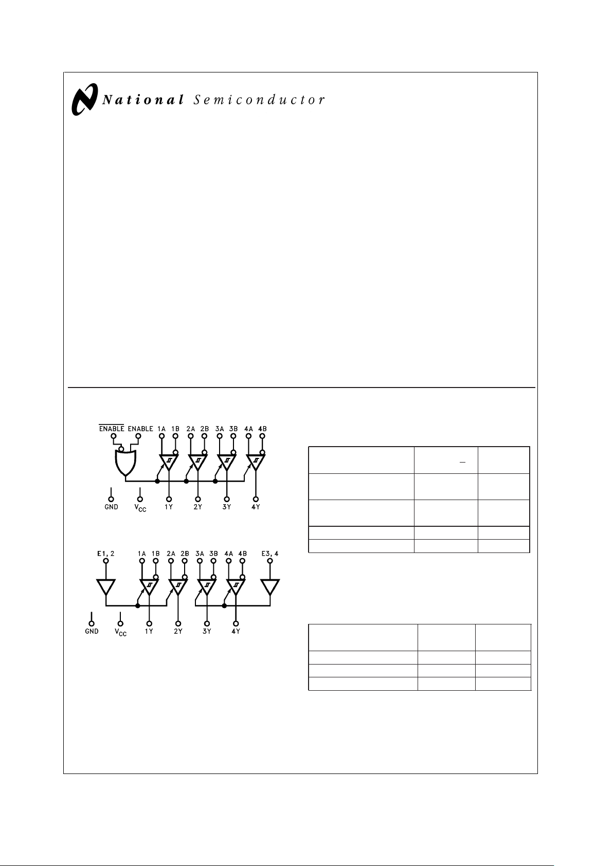
Logic Diagrams Function Tables
(Each Receiver) DS96F173
Differential Inputs Enable Output
A–B E E
Y
V
ID
≥ 0.2V H X H
XL H
V
ID
≤ −0.2V H X L
XL L
XLXZ
XXHZ
H = High Level
L = Low Level
Z = High Impedance (off)
X = Don’t Care
(Each Receiver) DS96F175
Differential Inputs Enable Output
A–B E Y
V
ID
≥ 0.2V H H
V
ID
≤ −0.2V H L
XLZ
TRI-STATE®is a registered trademark of National Semiconductor Corporation.
DS009627-10
DS96F175
DS009627-11
July 2000
DS96F173M/DS96F175C/DS96F175M EIA-485/EIA-422 Quad Differential Receivers
© 2000 National Semiconductor Corporation DS009627 www.national.com
COMMERCIAL
Absolute Maximum Ratings
(Note 2)
Specifications for the 883 version of this product are
listed separately.
Storage Temperature Range (T
STG
) −65˚C to +175˚C
Lead Temperature
(Soldering, 60 sec.) 300˚C
Max. Package Power Dissipation (Note 1) at 25˚C
Ceramic DIP (J) 1500 mW
Supply Voltage 7.0V
Input Voltage, A or B Inputs
±
25V
Differential Input Voltage
±
25V
Enable Input Voltage 7.0V
Low Level Output Current 50 mA
Recommended Operating
Conditions
Min Typ Max Units
Supply Voltage (V
CC
)
DS96F175C 4.75 5.0 5.25 V
Common Mode Input
Voltage (V
CM
) −7 +12 V
Differential Input Voltage
(V
ID
)
|12| V
Output Current HIGH (I
OH
) −400 µA
Output Current LOW (I
OL
)11mA
Operating Temperature (T
A
)
DS96F175C 0 25 70 ˚C
Note 1: Derate package 10 mW/˚C above 25˚C.
Electrical Characteristics (Notes 3, 4)
Over recommended supply voltage and operating temperature ranges, unless otherwise specified
Symbol Parameter Conditions Min Typ Max Units
V
TH
Differential-Input VO=V
OH
0.2 V
High Threshold Voltage
V
TL
Differential-Input (Note 5) VO=V
OL
−0.2 V
Low Threshold Voltage
V
TH−VTL
Hysteresis (Note 6) VCM=0V 50 mV
V
IH
Enable Input Voltage HIGH 2.0 V
V
IL
Enable Input Voltage LOW 0.8 V
V
IC
Enable Input Clamp Voltage II= −18 mA −1.5 V
V
OH
Output Voltage HIGH VID= 200 mV 0˚C to +70˚C 2.8
V
I
OH
= −400 µA −55˚C to +125˚C 2.5
V
OL
Output Voltage LOW VID= −200 mV IOL= 8.0 mA 0.45
V
I
OL
= 11 mA 0.50
I
OZ
High-Impedance State Output VO= 0.4V to 2.4V
±
20 µA
I
I
Line Input Current (Note 7) Other Input = 0V VI= 12V 1.0 mA
V
I
= −7.0V −0.8
I
IH
Enable Input Current HIGH VIH= 2.7V 20 µA
I
IL
Enable Input Current LOW VIL= 0.4V −100 µA
R
I
Input Resistance 14 18 22 kΩ
I
OS
Short Circuit Output Current (Note 8) −15 −85 mA
I
CC
Supply Current No Load Outputs Enabled 50
mA
I
CCX
Outputs Disabled 50
COMMERCIAL
Switching Characteristics
VCC= 5.0V, TA= 25˚C
Symbol Parameter Conditions Min Typ Max Units
t
PLH
Propagation Delay Time, VID= −2.5V to +2.5V, 5.0 15 22 ns
Low to High Level Output C
L
=15pF,
Figure 1
t
PHL
Propagation Delay Time, VCM= 0V 5.0 15 22 ns
High to Low Level Output
t
ZH
Output Enable Time to High Level CL=15pF,
Figure 2
12 16 ns
t
ZL
Output Enable Time to Low Level CL=15pF,
Figure 3
13 18 ns
t
HZ
Output Disable Time from High Level CL= 5.0 pF,
Figure 2
14 20 ns
DS96F173M/DS96F175C/DS96F175M
www.national.com 2
Switching Characteristics (Continued)
VCC= 5.0V, TA= 25˚C
Symbol Parameter Conditions Min Typ Max Units
t
LZ
Output Disable Time from Low Level CL= 5.0 pF,
Figure 3
14 18 ns
|t
PLH–tPHL
| Pulse Width Distortion (SKEW)
Figure 1
1.0 3.0 ns
Note 2: “Absolute Maximum Ratings” are those values beyond which the safety of the device cannot be guaranteed. They are not meant to imply that the devices
should be operated at these limits. The tables of “Electrical Characteristics” provide conditions for actual device operation.
Note 3: Unless otherwise specified min/max limits apply across the 0˚C to +70˚C range for the DS96F175C. All typicals are given for V
CC
= 5V and TA= 25˚C.
Note 4: All currents into the device pins are positive; all currents out of the device pins are negative. All voltages are reference to ground unless otherwise specified.
Note 5: The algebraic convention, when the less positive (more negative) limit is designated minimum, is used in this data sheet for common mode input voltage
and threshold voltage levels only.
Note 6: Hysteresis is the difference between the positive-going input threshold voltage. V
TH
, and the negative going input threshold voltage, VTL.
Note 7: Refer to EIA-485 Standard for exact conditions.
Note 8: Only one output at a time should be shorted.
Order Number: DS96F175CJ
See NS Package Number J16A
DS96F173M/DS96F175C/DS96F175M
www.national.com3

MIL-STD-883C
Absolute Maximum Ratings
(Note 2)
For complete Military Specifications, refer to the appropriate SMD or MDS.
Storage Temperature Range (T
STG
) −65˚C to +175˚C
Lead Temperature
(Soldering, 60 sec.) 300˚C
Max. Package Power Dissipation (Note 9) at 25˚C
Ceramic DIP (J) 1500 mW
Ceramic Flatpak (W) 1034 mW
Ceramic LCC (E) 1500 mW
Supply Voltage 7.0V
Input Voltage, A or B Inputs
±
25V
Differential Input Voltage
±
25V
Enable Input Voltage 7.0V
Low Level Output Current 50 mA
Recommended Operating
Conditions
Min Typ Max Units
Supply Voltage (V
CC
)
DS96F173M/DS96F175M 4.50 5.0 5.50 V
Common Mode
Input Voltage (V
CM
)
−7 +12 V
Differential Input Voltage (V
ID
) |12| V
Output Current HIGH (I
OH
) −400 µA
Output Current LOW (I
OL
)11mA
Operating Temperature (T
A
)
DS96F173M/DS96F175M −55 25 125 ˚C
Note 9: Above TA= 25˚C derate J package 10 mW/˚C, W package
6.90 mW/˚C, E package 11.11 mW/˚C.
Electrical Characteristics (Notes 3, 4)
Over recommended supply voltage and operating temperature ranges, unless otherwise specified
Symbol Parameter Conditions Min Max Units
V
TH
Differential-Input
High Threshold Voltage
VCC= 4.5V, 5.5V
V
CM
= 0V, 12V, −12V
0.2 V
V
TL
Differential-Input (Note 5)
Low Threshold Voltage
VCC= 4.5V, 5.5V
V
CM
= 0V, 12V, −12V
−0.2 V
V
IH
Enable Input Voltage HIGH 2.0 V
V
IL
Enable Input Voltage LOW 0.8 V
V
IC
Enable Input Clamp Voltage II= −18 mA, VCC= 4.5V −1.5 V
V
OH
Output Voltage HIGH VID= 200 mV
I
OH
= −400 µA
−55˚C to +125˚C
2.5 V
V
OL
Output Voltage LOW VID= −200 mV IOL= 8.0 mA 0.45 V
I
OZ
High-Impedance State Output VO= 0.4V, 2.4V, VCC= 5.5V
±
20 µA
I
I
Line Input Current (Note 7) Other Input = 0V VI= 12V 1.0
mA
V
I
= −7.0V −0.8
I
IH
Enable Input Current HIGH VIH= 2.7V, VCC= 5.5V 20 µA
I
IL
Enable Input Current LOW VIL= 0.4V, VCC= 5.5V −100 µA
R
I
Input Resistance 10 kΩ
I
OS
Short Circuit Output Current (Note 8) −15 −85 mA
I
CC
Supply Current No Load Outputs Enabled
or Disabled
50 mA
I
CCX
MIL-STD-883C
Switching Characteristics
VCC= 5.0V
Symbol Parameter Conditions T
A
= 25˚C TA= −55˚C TA=
125˚C
Units
Typ Max Max Max
t
PLH
Propagation Delay Time, VID= −2.5V to +2.5V, 15 22 30 30 ns
Low to High Level Output C
L
=15pF,
Figure 1
t
PHL
Propagation Delay Time, VCM=0V 15 22 30 30 ns
High to Low Level Output
t
ZH
Output Enable Time to High
Level
CL=15pF,
Figure 2
12 16 27 27 ns
DS96F173M/DS96F175C/DS96F175M
www.national.com 4

Switching Characteristics (Continued)
VCC= 5.0V
Symbol Parameter Conditions T
A
= 25˚C TA= −55˚C TA=
125˚C
Units
Typ Max Max Max
t
ZL
Output Enable Time to Low
Level
CL=15pF,
Figure 3
13 18 27 27 ns
t
HZ
Output Disable Time from High
Level
CL= 5.0 pF,
Figure 2
(Note 15) 14 20 27 27 ns
C
L
=20pF,
Figure 2
(Note 15) 14 30 37 37 ns
t
LZ
Output Disable Time from Low
Level
CL= 5.0 pF,
Figure 3
14 18 30 30 ns
|t
PLH–tPHL
| Pulse Width Distortion (SKEW)
Figure 1
1 3 5.0 5.0 ns
SMD Number: DS96F173MJ 5962-9076602 MEA
DS96F173MW 5962-9076602 MFA
DS96F173ME 5962-9076602 M2A
DS96F175MJ 5962-9076601 MEA
DS96F175MW 5962-9076601 MFA
DS96F175ME 5962-9076601 M2A
Order Number: 883 Marking SMD Marking
DS96F173MJ/883 DS96F173MJ-SMD
DS96F175MJ/883 DS96F175MJ-SMD
See NS Package Number
J16A
DS96F173ME/883 DS96F173ME-SMD
DS96F175ME/883 DS96F175ME-SMD
See NS Package Number
E20A
DS96F173MW/883 DS96F173MW-SMD
DS96F175MW/883 DS96F175MW-SMD
See NS Package Number
W16A
For complete Military Product Specifications, refer
to the appropriate SMD or MDS.
DS96F173M/DS96F175C/DS96F175M
www.national.com5

Connection Diagrams
16-Lead Ceramic Dual-In-Line Package
NS Package Number J16A
DS96F173
DS009627-1
Top View
DS96F175
DS009627-2
Top View
20-Lead Ceramic Leadless Chip Carrier
NS Package Number E20A
DS009627-12
*NC—No Connection
Top View
DS009627-13
Top View
DS96F173M/DS96F175C/DS96F175M
www.national.com 6

Connection Diagrams (Continued)
Order Numbers are located at the end of the respective Electrical Tables.
Parameter Measurement Information
16-Lead Ceramic Flatpak
NS Package Number W16A
DS009627-14
Top View
DS009627-15
Top View
DS009627-3
DS009627-4
FIGURE 1. t
PLH,tPHL
(Notes 10, 11)
DS009627-5
DS009627-6
FIGURE 2. tHZ,tZH(Notes 10, 11, 13, 14)
DS96F173M/DS96F175C/DS96F175M
www.national.com7

Parameter Measurement Information (Continued)
Note 10: The input pulse is supplied by a generator having the following characteristics: f = 1.0 MHz, 50% duty cycle, tr≤ 6.0 ns, tf≤ 6.0 ns, ZO=50Ω.
Note 11: C
L
includes probe and stray capacitance.
Note 12: DS96F173 with active high and active low Enables are shown. DS96F175 has active high Enable only.
Note 13: All diodes are 1N916 or equivalent.
Note 14: To test the active low Enable E of DS96F173, ground E and apply an inverted input waveform to E . DS96F175 has active high enable only.
Note 15: Testing at 20 pF assures conformance to 5 pF specification.
Typical Application
Note: The line length should be terminated at both ends in its characteristic impedance. Stub lengths off the main line should be kept as short as possible.
DS009627-7
DS009627-8
FIGURE 3. tZL,tLZ(Notes 10, 11, 13, 14)
DS009627-9
FIGURE 4.
DS96F173M/DS96F175C/DS96F175M
www.national.com 8

Physical Dimensions inches (millimeters) unless otherwise noted
20-Lead Ceramic Leadless Chip Carrier (E)
Order Number DS96F173ME/883 or DS96F175ME/883
NS Package Number E20A
16-Lead Ceramic Dual-In-Line Package (J)
Order Number DS96F175CJ, DS96F173MJ/883 or DS96F175MJ/883
NS Package Number J16A
DS96F173M/DS96F175C/DS96F175M
www.national.com9

Physical Dimensions inches (millimeters) unless otherwise noted (Continued)
LIFE SUPPORT POLICY
NATIONAL’S PRODUCTS ARE NOT AUTHORIZED FOR USE AS CRITICAL COMPONENTS IN LIFE SUPPORT
DEVICES OR SYSTEMS WITHOUT THE EXPRESS WRITTEN APPROVAL OF THE PRESIDENT AND GENERAL
COUNSEL OF NATIONAL SEMICONDUCTOR CORPORATION. As used herein:
1. Life support devices or systems are devices or
systems which, (a) are intended for surgical implant
into the body, or (b) support or sustain life, and
whose failure to perform when properly used in
accordance with instructions for use provided in the
labeling, can be reasonably expected to result in a
significant injury to the user.
2. A critical component is any component of a life
support device or system whose failure to perform
can be reasonably expected to cause the failure of
the life support device or system, or to affect its
safety or effectiveness.
National Semiconductor
Corporation
Americas
Tel: 1-800-272-9959
Fax: 1-800-737-7018
Email: support@nsc.com
National Semiconductor
Europe
Fax: +49 (0) 180-530 85 86
Email: europe.support@nsc.com
Deutsch Tel: +49 (0) 69 9508 6208
English Tel: +44 (0) 870 24 0 2171
Français Tel: +33 (0) 1 41 91 8790
National Semiconductor
Asia Pacific Customer
Response Group
Tel: 65-2544466
Fax: 65-2504466
Email: ap.support@nsc.com
National Semiconductor
Japan Ltd.
Tel: 81-3-5639-7560
Fax: 81-3-5639-7507
www.national.com
16-Lead Ceramic FlatPak (W)
Order Number DS96F173MW/883 or DS96F175MW/883
NS Package Number W16A
DS96F173M/DS96F175C/DS96F175M EIA-485/EIA-422 Quad Differential Receivers
National does not assume any responsibility for use of any circuitry described, no circuit patent licenses are implied and National reserves the right at any time without notice to change said circuitry and specifications.
 Loading...