

NSC DS92CK16TMTCX, DS92CK16TMTC Datasheet

DS92CK16
3V BLVDS 1 to 6 Clock Buffer/Bus Transceiver
General Description
The DS92CK16 1 to 6 Clock Buffer/Bus Transceiverisaone
to sixCMOSdifferential clock distributiondeviceutilizingBus
Low Voltage Differential Signaling (BLVDS) technology.This
clock distribution device is designed for applications requiring ultra low power dissipation, low noise, and high data
rates. The BLVDS side is a transceiver with a separate channel acting as a return/source clock.
The DS92CK16 accepts BLVDS (300 mV typical) differential
input levels, and translates them to 3V CMOS output levels.
An output enable pin OE , when high, forces all CLK
OUT
pins
high.
The device can be used a source synchronous driver. The
selection of the source driving is controlled by the CrdCLK
IN
and DE pins. This device can be the master clock, driving the
inputs of other clock I/O pins in a multipoint environment.
Easy master/slave clock selection is achieved along a backplane.
Features
n Master/Slave clock selection in a backplane application
n 125 MHz operation (typical)
n 100 ps duty cycle distortion (typical)
n 50 ps channel to channel skew (typical)
n 3.3V power supply design
n Glitch-free power on at CLKI/O pins
n Low Power design (20 mA
@
3.3V static)
n Accepts small swing (300 mV typical) differential signal
levels
n Industrial temperature operating range (-40˚C to +85˚C)
n Available in 24-pin TSSOP Packaging
Function Diagram and Truth Table
Receive Mode Truth Table
INPUT OUTPUT
OE
DE CrdCLKIN(CLKI/O+)–(CLKI/O−) CLK
OUT
HH X X H
L H X VID≥ 0.07V H
L H X VID≤ −0.07V L
L=Low Logic State
H=High Logic State
X=Irrelevant
Z=TRI-STATE
Driver Mode Truth Table
INPUT OUTPUT
OE
DE CrdCLKINCLK/I/O+ CLKI/O− CLK
OUT
LL L L H L
LL H H L H
HL L L H H
HL H H L H
HH X Z Z H
TRI-STATE®is a registered trademark of National Semiconductor Corporation.
DS101082-1
November 1999
DS92CK16 3V BLVDS 1 to 6 Clock Buffer/Bus Transceiver
© 1999 National Semiconductor Corporation DS101082 www.national.com
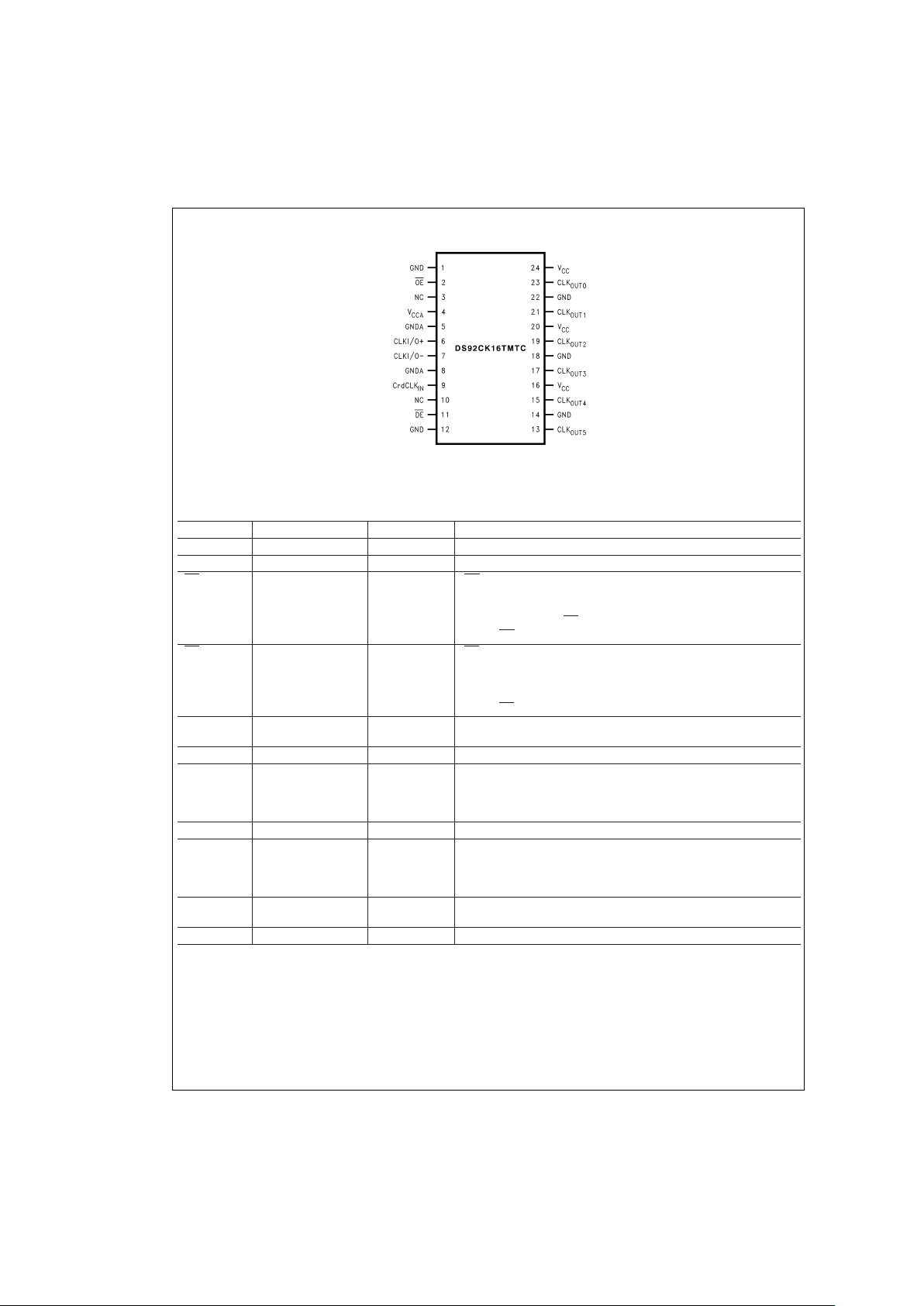
Connection Diagram
TSSOP Package Pin Description
Pin Name Pin # Type Description
CLKI/O+ 6 I/O True (Positive) side of the differential clock input.
CLKI/O− 7 I/O Complementary (Negative) side of the differential clock input.
OE
2 I OE; this pin is active Low. When High, this pin forces all CLK
OUT
pins High. When Low, CLK
OUT
pins logic state is determined by
either the CrdCLK
IN
or the VID at the CLK/I/O pins with respect to
the logic level at the DE pin. This pin has a weak pullup device to
VCC. If OE is floating, then all CLK
OUT
pins will be High.
DE 11 I DE; this pin is active LOW. When Low, this pin enables the
CardCLKINsignal to the CLKI/O pins and CLK
OUT
pins. When High,
the Driver is TRI-STATE
®
, the CLKI/O pins are inputs and determine
the state of the CLK
OUT
pins. This pin has a weak pullup device to
V
CC
. If DE is floating, then CLKI/O pins are TRI-STATE.
CLK
OUT
13, 15, 17, 19, 21,
23
O 6 Buffered clock (CMOS) outputs.
CrdCLK
IN
9 I Input clock from Card (CMOS level or TTL level).
V
CC
16, 20, 24 Power VCC; Analog V
CCA
(Internally separate from VCC, connect externally
or use separate power supplies). No special power sequencing
required. Either V
CCA
or VCCcan be applied first, or simultaneously
apply both power supplies.
GND 1, 12, 14, 18, 22 Ground GND
V
CCA
4 Power Analog V
CCA
(Internally separate from VCC, connect externally or use
separate power supplies). No special power sequencing required.
Either V
CCA
or VCCcan be applied first, or simultaneously apply both
power supplies.
GNDA 5, 8 Ground Analog Ground (Internally separate from Ground must be connected
externally).
NC 3, 10 No Connects
DS101082-2
Order Number DS92CK16TMTC
See NS Package Number MTC24
DS92CK16
www.national.com 2
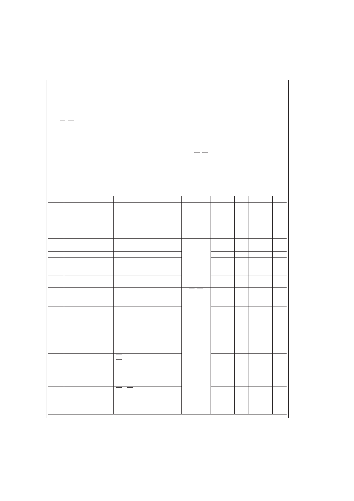
Absolute Maximum Ratings (Note 1)
If Military/Aerospace specified devices are required,
please contact the National Semiconductor Sales Office/
Distributors for availability and specifications.
Supply Voltage (V
CC
) −0.3V to +4V
Enable Input Voltage
(DE, OE, CrdCLK
IN
) −0.3V to +4V
Voltage (CLK
OUT
) −0.3V to (VCC+ 0.3V)
Voltage (CLKI/O
±
) −0.3V to +4V
Driver Short Circuit Current momentary
Receiver Short Circuit Current momentary
Maximum Package Power Dissipation at +25˚C
TSSOP Package 1500 mW
Derate TSSOP Package 8.2 mW/˚C above +25˚C
θ
JA
95˚C/W
θ
JC
30˚C/W
Storage Temperature Range −65˚C to +150˚C
Lead Temperature Range
(Soldering, 4 sec.) 260˚C
ESD Ratings: HBM (Note 2)
>
3000V
CDM (Note 2)
>
1000V
Machine Model (Note 2)
>
200V
Recommended Operating
Conditions
Min Typ Max Units
Supply Voltage (V
CC
) +3.0 +3.3 +3.6 V
CrdCLK
IN
, DE, OE
Input Voltage 0 V
CC
V
Operating Free Air
Temperature (T
A
) −40 25 +85 ˚C
DC Electrical Characteristics
Over Supply Voltage and Operating Temperature ranges, unless otherwise specified (Notes 3, 4).
Symbol Parameter Conditions Pin Min Typ Max Units
V
TH
Input Threshold High CLKI/O+,
CLKI/O−
25 +70 mV
V
TL
Input Threshold Low −70 -35 mV
VCMR Common Mode Voltage
Range (Note 5)
VID=250 mV pk to pk
|VID|/2
2.4 -
|VID|/2
V
I
IN
Input Current V
IN
=
0V to V
CC
,DE=VCC,OE
=
VCC, Other Input=1.2V±50 mV
−20
±
5 +20 µA
V
OH1R
Output High Voltage VID=250 mV, I
OH
=
−1.0 mA CLK
OUT
VCC−0.4 2.9 V
V
OH2R
Output High Voltage VID=250 mV, I
OH
=
−6 mA V
CC
−0.8 2.5 V
V
OL1R
Output Low Voltage I
OL
=
1.0 mA, VID=−250 mV 0.06 0.3 V
V
OL2R
Output Low Voltage I
OL
=
6 mA, VID=−250 mV 0 0.4 V
I
ODHR
CLK
OUT
Dynamic
Output Current (Note 6)
VID=+250 mV, V
OUT
=
V
CC
−1V
−8 -16 -30 mA
I
ODLR
CLK
OUT
Dynamic
Output Current (Note 6)
VID=−250 mV, V
OUT
=
1V
10 21 35 mA
V
IH
Input High Voltage DE, OE,
CrdCLK
IN
2.0 V
CC
V
V
IL
Input Low Voltage GND 0.8 V
I
IH
Input High Current V
IN
=
V
CC
or 2.4V OE, DE −10 −2 +10 µA
I
IL
Input Low Current V
IN
=
GND or 0.4V −20 −5 +20 µA
I
INCRD
Input Current V
IN
=
0V to V
CC
,OE=V
CC
CrdCLK
IN
−5 +5 µA
V
CL
Input Voltage Clamp I
OUT
=
−1.5 mA OE, DE,
CrdCLK
IN
−0.8 V
I
CC
No Load Supply Current
Outputs Enabled, No
VID Applied
OE=DE=0V,
CrdCLK
IN
=
V
CC
or GND,
CLKI/O (
±
)=Open
CLK
OUT
(0:5)=Open Circuit
V
CC
13 mA
I
CC1
No Load Supply Current
Outputs Enabled, VID
over Common Mode
Voltage Range
OE=GND
DE=V
CC
CrdCLK
IN
=
V
CC
or GND,
VID=250 mV
(0.125V VCM 2.275V),
CLK
OUT
(0:5)=Open Circuit
10 mA
I
CCD
Driver Loaded Supply
Current
DE=OE=0V,
CrdCLK
IN
=
V
CC
or GND,
R
L
=
37.5Ω between CLKI/O+ and
CLKI/O−,
CLK
OUT
(0:5)=Open Circuit
20 25 mA
DS92CK16
www.national.com3

DC Electrical Characteristics (Continued)
Over Supply Voltage and Operating Temperature ranges, unless otherwise specified (Notes 3, 4).
Symbol Parameter Conditions Pin Min Typ Max Units
V
OD
Driver Output Differential
Voltage
R
L
=
37.5Ω,
Figure 5
DE=0V
CLKI/O+,
CLKI/O−
250 350 450 mV
∆V
OD
Driver VODMagnitude
Change
10 20 mV
V
OS
Driver Offset Voltage 1.1 1.29 1.5 V
∆V
OS
Driver Offset Voltage
Magnitude Change
520mV
V
OHD
Driver Output High 1.35 1.8 V
V
OLD
Driver Output Low 0.80 1.05 V
I
OS1D
Driver Differential Short
Circuit Current (Note 6)
CrdCLK
IN
=
V
CC
or GND, VOD
=
0V, (outputs shorted together)
DE=0V
|30| |50| mA
I
OS2D
Driver Output Short
Circuit Current to V
CC
(Note 6)
CrdCLK
IN
=
GND, DE=0V,
CLKI/O+=V
CC
36 70 mA
I
OS3D
Driver Output Short
Circuit Current to V
CC
(Note 6)
CrdCLK
IN
=
V
CC
,DE=0V,
CLKI/O−=V
CC
34 70 mA
I
OS4D
Driver Output Short
Circuit Current to GND
(Note 6)
CrdCLK
IN
=
V
CC
,DE=0V,
CLKI/O+=0V −47 −70 mA
I
OS5D
Driver Output Short
Circuit Current to GND
(Note 6)
CrdCLK
IN
=
GND, DE=0V,
CLKI/O−=0V −50 −70 mA
I
OFF
Power Off Leakage
Current
V
CC
=
0V or Open,
V
APPLIED
=
3.6V
±
20 µA
Switching Characteristics
Over Supply Voltage and Operating Temperature ranges, unless otherwise specified (Notes 7, 8).
Symbol Parameter Conditions Min Typ Max Units
DIFFERENTIAL RECEIVER CHARACTERISTICS
t
PHLDR
Differential Propagation Delay High to Low. CLKI/O to
CLK
OUT
C
L
=
15 pF
VID=250 mV
Figures 1, 2
1.3 2.8 3.8 ns
t
PLHDR
Differential Propagation Delay Low to High. CLKI/O to
CLK
OUT
1.3 2.9 3.8 ns
t
SK1R
Duty Cycle Distortion(Note 10)
(pulse skew)
|t
PLH–tPHL
|
100 400 ps
t
SK2R
Channel to Channel Skew; Same Edge (Note 11) 30 80 ps
t
SK3R
Part to Part Skew (Note 12) 2.5 ns
t
TLHR
Transition Time Low to High (Note 9)
(20%to 80%)
0.4 1.4 2.4 ns
t
THLR
Transition Time High to Low(Note 9)
(80%to 20%)
0.4 1.3 2.2 ns
t
PLHOER
Propagation Delay Low to High
( OEto CLK
OUT
)
C
L
=
15 pF
Figures 3, 4
1.0 3 4.5 ns
t
PHLOER
Propagation Delay High to Low
(OE to CLK
OUT
)
1.0 3 4.5 ns
f
MAX
Maximum Operating Frequency (Note 15) 100 125 MHz
DS92CK16
www.national.com 4
 Loading...