

DS90CR583/DS90CR584
LVDS 24-Bit Color Flat Panel Display (FPD) Link—
65 MHz
General Description
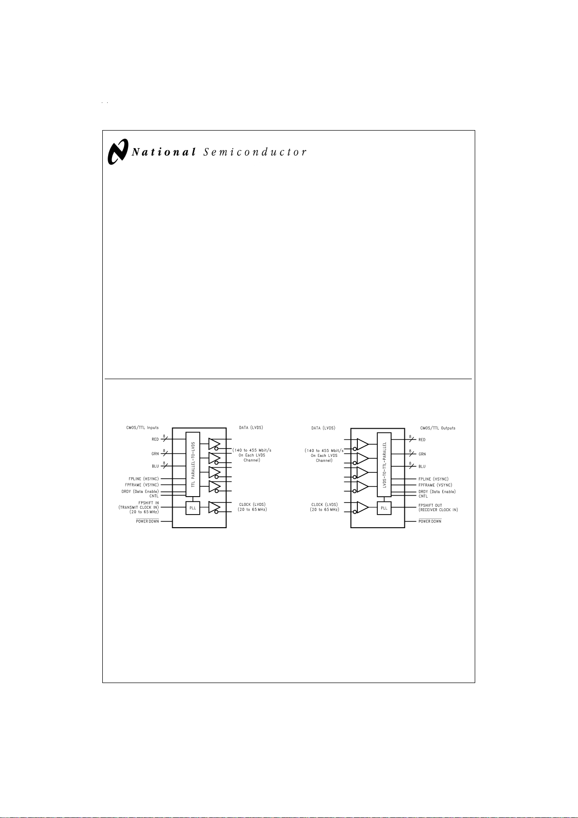
The DS90CR583 transmitter converts 28 bits of CMOS/TTL
data into four LVDS(Low Voltage Differential Signaling) data
streams. A phase-locked transmit clock is transmitted in parallel with the data streams over a fifth LVDS link. Every cycle
of the transmit clock 28 bits of input data are sampled and
transmitted. The DS90CR584 receiver converts the LVDS
data streams back into 28 bits of CMOS/TTLdata.At a transmit clock frequency of 65 MHz, 24 bits of RGB data and 4
bits of LCD timing and control data (FPLINE, FPFRAME,
DRDY, CONTROL) are transmitted at a rate of 455 Mbps per
LVDSdata channel. Using a 65 MHz clock, the data throughput is 227 Mbytes per second. These devices are offered
with rising edge data strobes for convenient interface with a
variety of graphics and LCD panel controllers.
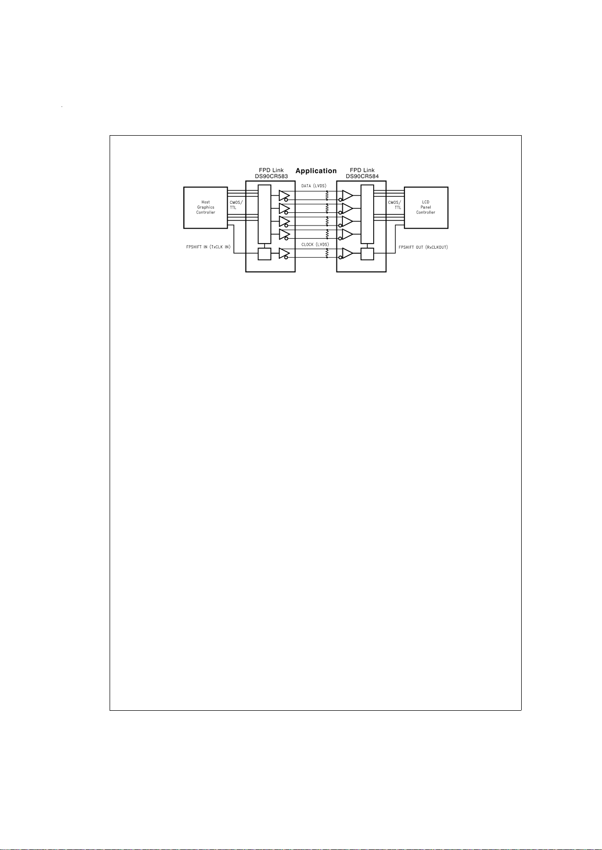
This chipset is an ideal means to solve EMI and cable size
problems associated with wide, high speed TTL interfaces.
Features
n 20 to 65 MHz shift clk support
n Up to 227 Mbytes/s bandwidth
n Cable size is reduced to save cost
n 290 mV swing LVDS devices for low EMI
n Low power CMOS design (
<
550 mW typ)
n Power-down mode saves power (
<
0.25 mW)
n PLL requires no external components
n Low profile 56-lead TSSOP package
n Rising edge data strobe
n Compatible with TIA/EIA-644 LVDS standard
n Single pixel per clock XGA (1024 x 768)
n Supports VGA, SVGA, XGA and higher
n 1.8 Gbps throughput
Block Diagrams
TRI-STATE®is a registered trademark of National Semiconductor Corporation.
DS90CR583
DS012618-2
Order Number DS90CR583MTD
See NS Package Number MTD56
DS90CR584
DS012618-1
Order Number DS90CR584MTD
See NS Package Number MTD56
July 1997
DS90CR583/DS90CR584 LVDS 24-Bit Color Flat Panel Display (FPD) Link—65 MHz
© 1998 National Semiconductor Corporation DS012618 www.national.com
Block Diagrams (Continued)
DS012618-3
www.national.com 2
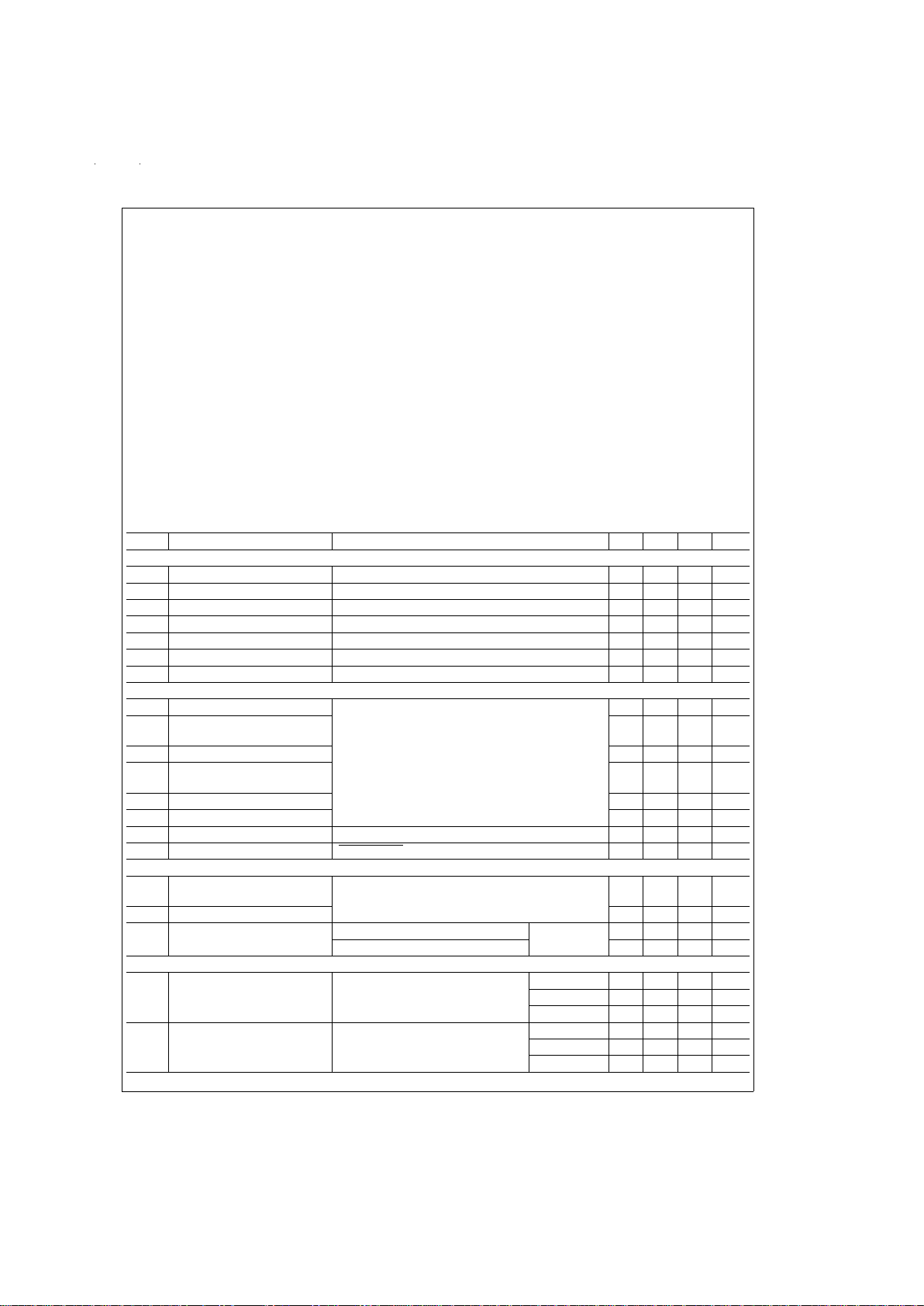
Absolute Maximum Ratings (Note 1)
If Military/Aerospace specified devices are required,
please contact the National Semiconductor Sales Office/
Distributors for availability and specifications.
Supply Voltage (V
CC
) −0.3V to +6V
CMOS/TTL Input Voltage −0.3V to (V
CC
+ 0.3V)
CMOS/TTL Output Voltage −0.3V to (V
CC
+ 0.3V)
LVDS Receiver Input Voltage −0.3V to (V
CC
+ 0.3V)
LVDS Driver Output Voltage −0.3V to (V
CC
+ 0.3V)
LVDS Output Short Circuit
Duration Continuous
Junction Temperature +150˚C
Storage Temperature −65˚C to +150˚C
Lead Temperature
(Soldering, 4 sec) +260˚C
Maximum Power Dissipation
@
25˚C
MTD56 (TSSOP) Package:
DS90CR583 1.63W
DS90CR584 1.61W
Package Derating:
DS90CR583 12.5 mW/˚C above +25˚C
DS90CR584 12.4 mW/˚C above +25˚C
This device does not meet 2000V ESD rating (Note 4) .
Recommended Operating
Conditions
Min Nom Max Units
Supply Voltage (V
CC
) 4.75 5.0 5.25 V
Operating Free Air −10 +25 +70 ˚C
Temperature (T
A
)
Receiver Input Range 0 2.4 V
Supply Noise Voltage (V
CC
) 100 mV
P-P
Electrical Characteristics
Over recommended operating supply and temperature ranges unless otherwise specified
Symbol Parameter Conditions Min Typ Max Units
CMOS/TTL DC SPECIFICATIONS
V
IH
High Level Input Voltage 2.0 V
CC
V
V
IL
Low Level Input Voltage GND 0.8 V
V
OH
High Level Output Voltage I
OH
=
−0.4 mA 3.8 4.9 V
V
OL
Low Level Output Voltage I
OL
=
2 mA 0.1 0.3 V
V
CL
Input Clamp Voltage I
CL
=
−18 mA −0.79 −1.5 V
I
IN
Input Current V
IN
=
V
CC
, GND, 2.5V or 0.4V
±
5.1±10 µA
I
OS
Output Short Circuit Current V
OUT
=
0V −120 mA
LVDS DRIVER DC SPECIFICATIONS
V
OD
Differential Output Voltage R
L
=
100Ω 250 290 450 mV
∆V
OD
Change in VODbetween
Complementary Output States
35 mV
V
CM
Common Mode Voltage 1.1 1.25 1.375 V
∆V
CM
Change in VCMbetween
Complementary Output States
35 mV
V
OH
High Level Output Voltage 1.3 1.6 V
V
OL
Low Level Output Voltage 0.9 1.01 V
I
OS
Output Short Circuit Current V
OUT
=
0V, R
L
=
100Ω −2.9 −5 mA
I
OZ
Output TRI-STATE®Current Power Down=0V, V
OUT
=
0V or V
CC
±1±
10 µA
LVDS RECEIVER DC SPECIFICATIONS
V
TH
Differential Input High
Threshold
V
CM
=
+1.2V +100 mV
V
TL
Differential Input Low Threshold −100 mV
I
IN
Input Current V
IN
=
+2.4V V
CC
=
5.5V
±
10 µA
V
IN
=
0V
±
10 µA
TRANSMITTER SUPPLY CURRENT
I
CCTW
Transmitter Supply Current,
Worst Case
R
L
=
100Ω,C
L
=
5 pF,
Worst Case Pattern
(
Figure 1,Figure 3
)
f=32.5 MHz 49 63 mA
f=37.5 MHz 51 64 mA
f=65 MHz 70 84 mA
I
CCTG
Transmitter Supply Current,
16 Grayscale
R
L
=
100Ω,C
L
=
5 pF,
16 Grayscale Pattern
(
Figure 2,Figure 3
)
f=32.5 MHz 40 55 mA
f=37.5 MHz 41 55 mA
f=65 MHz 55 67 mA
www.national.com3
Electrical Characteristics (Continued)
Over recommended operating supply and temperature ranges unless otherwise specified
Symbol Parameter Conditions Min Typ Max Units
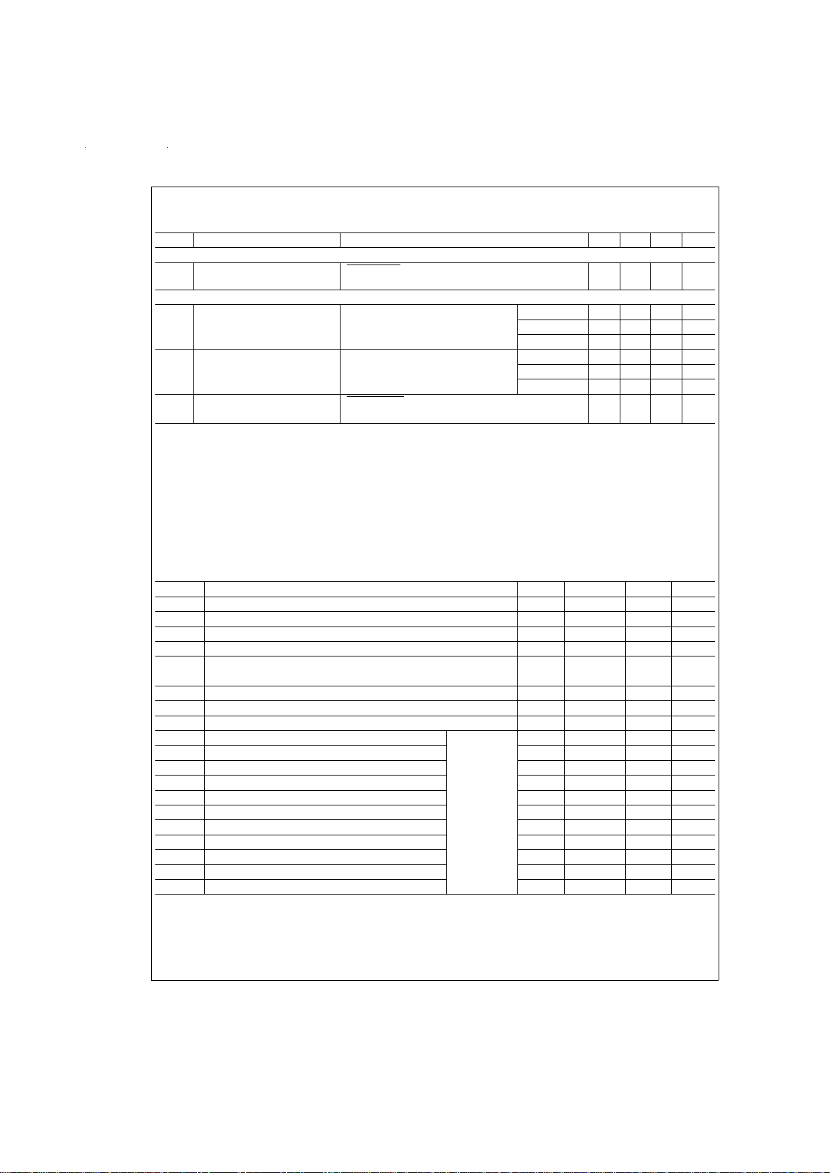
TRANSMITTER SUPPLY CURRENT
I
CCTZ
Transmitter Supply Current,
Power Down
Power Down=Low 125µA
RECEIVER SUPPLY CURRENT
I
CCRW
Receiver Supply Current, C
L
=
8 pF, f=32.5 MHz 64 77 mA
Worst Case Worst Case Pattern f=37.5 MHz 70 85 mA
(
Figure 1,Figure 4
)f
=
65 MHz 110 140 mA
I
CCRG
Receiver Supply Current, C
L
=
8 pF, f=32.5 MHz 35 55 mA
16 Grayscale 16 Grayscale Pattern f=37.5 MHz 37 55 mA
(
Figure 2,Figure 4
)f
=
65 MHz 55 67 mA
I
CCRZ
Receiver Supply Current, Power Down=Low 110µA
Power Down
Note 1: “Absolute Maximum Ratings” are those values beyond which the safety of the device cannot be guaranteed. They are not meant to imply that the device
should be operated at these limits. The tables of “Electrical Characteristics” specify conditions for device operation.
Note 2: Typical values are given for V
CC
=
5.0V and T
A
=
+25˚C.
Note 3: Current into device pins is defined as positive. Current out of device pins is defined as negative. Voltages are referenced to ground unless otherwise specified (except V
OD
and ∆VOD).
Note 4: ESD Rating: HBM (1.5 kΩ, 100 pF)
PLL V
CC
≥ 1000V
All other pins ≥ 2000V
EIAJ (0Ω, 200 pF) ≥ 150V
Transmitter Switching Characteristics
Over recommended operating supply and temperature ranges unless otherwise specified
Symbol Parameter Min Typ Max Units
LLHT LVDS Low-to-High Transition Time (
Figure 3
) 0.75 1.5 ns
LHLT LVDS High-to-Low Transition Time (
Figure 3
) 0.75 1.5 ns
TCIT TxCLK IN Transition Time (
Figure 5
)8ns
TCCS TxOUT Channel-to-Channel Skew (Note 5) (
Figure 6
) 350 ps
TCCD TxCLK IN to TxCLK OUT Delay
@
25˚C, V
CC
=
5.0V 3.5 8.5 ns
(
Figure 9
)
TCIP TxCLK IN Period (
Figure 7
) 15 T 50 ns
TCIH TxCLK IN High Time (
Figure 7
) 0.35T 0.5T 0.65T ns
TCIL TxCLK IN Low Time (
Figure 7
) 0.35T 0.5T 0.65T ns
TSTC TxIN Setup to TxCLK IN (
Figure 7
)f
=
65 MHz 5 3.5 ns
THTC TxIN Hold to TxCLK IN (
Figure 7
) 2.5 1.5 ns
TPDD Transmitter Powerdown Delay (
Figure 18
) 100 ns
TPLLS Transmitter Phase Lock Loop Set (
Figure 11
)10ms
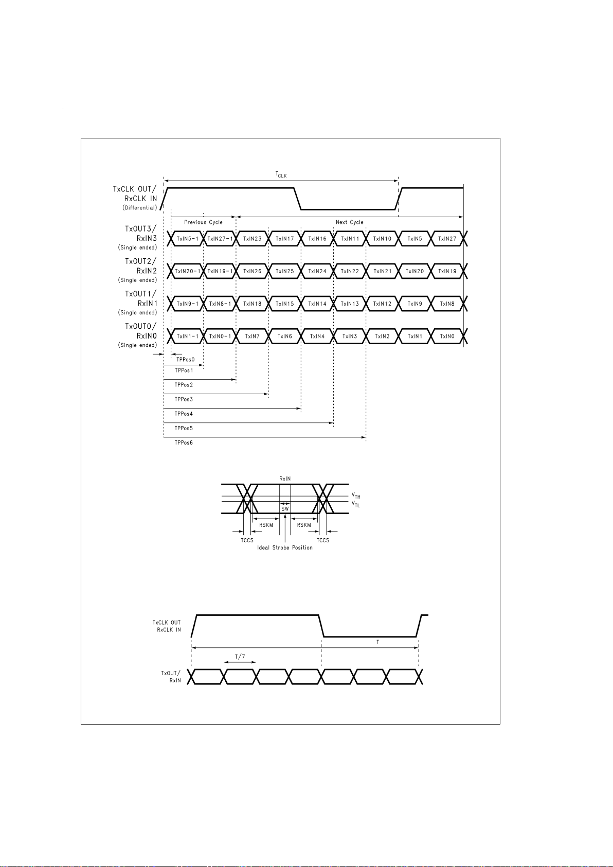
TPPos0 Transmitter Output Pulse Position 0 (
Figure 13
) −0.30 0 0.30 ns
TPPos1 Transmitter Output Pulse Position 1 1.70 1/7 T
clk
2.50 ns
TPPos2 Transmitter Output Pulse Position 2 3.60 2/7 T
clk
4.50 ns
TPPos3 Transmitter Output Pulse Position 3 5.90 3/7 T
clk
6.75 ns
TPPos4 Transmitter Output Pulse Position 4 8.30 4/7 T
clk
9.00 ns
TPPos5 Transmitter Output Pulse Position 5 10.40 5/7 T
clk
11.10 ns
TPPos6 Transmitter Output Pulse Position 6 12.70 6/7 T
clk
13.40 ns
Note 5: This limit based on bench characterization.
www.national.com 4

Receiver Switching Characteristics
Over recommended operating supply and temperature ranges unless otherwise specified.
Symbol Parameter Min Typ Max Units
CLHT CMOS/TTL Low-to-High Transition Time (
Figure 4
) 2.5 4.0 ns
CHLT CMOS/TTL High-to-Low Transition Time (
Figure 4
) 2.0 3.5 ns
RCOP RxCLK OUT Period 15 T 50 ns
RCOH RxCLK OUT High Time f=65 MHz 3.8 5 ns
RCOL RxCLK OUT Low Time f=65 MHz 7.8 9 ns
RSRC RxOUT Setup to RxCLK OUT f=65 MHz 2.5 4.2 ns
RHRC RxOUT Hold to RxCLK OUT f=65 MHz 4.0 5.2 ns
RCCD RxCLK IN to RxCLK OUT Delay
@
25˚C, V
CC
=
5.0V 6.4 10.7 ns
(
Figure 10
)
RPLLS Receiver Phase Lock Loop Set (
Figure 12
)10ms
RSKM RxIN Skew Margin (Note 6) (
Figure 14
)V
CC
=
5V, T
A
=
25˚C 600 ps
RPDD Receiver Powerdown (
Figure 17
)1µs
Note 6: Receiver Skew Margin is defined as the valid data sampling region at the receiver inputs. This margin takes into account transmitter output skew (TCCS)
and the setup and hold time (internal data sampling window), allowing for LVDS cable skew dependent on type/length and source clock (TxCLK IN) jitter.
RSKM ≥ cable skew (type, length) + source clock jitter (cycle to cycle)
AC Timing Diagrams
DS012618-4
FIGURE 1. “Worst Case” Test Pattern
www.national.com5

AC Timing Diagrams (Continued)
Note 7: The worst case test pattern produces a maximum toggling of digital circuits, LVDS I/O and CMOS/TTL I/O.
Note 8: The 16 grayscale test pattern tests device power consumption for a “typical” LCD display pattern. The test pattern approximates signal switching needed
to produce groups of 16 vertical stripes across the display.
Note 9:
Figure 1
and
Figure 2
show a falling edge data strobe (TxCLK IN/RxCLK OUT).
Note 10: Recommended pin to signal mapping. Customer may choose to define differently.
DS012618-5
FIGURE 2. “16 Grayscale” Test Pattern
DS012618-6
FIGURE 3. DS90CR583 (Transmitter) LVDS Output Load and Transition Times
DS012618-7
FIGURE 4. DS90CR584 (Receiver) CMOS/TTL Output Load and Transition Times
www.national.com 6

AC Timing Diagrams (Continued)
DS012618-8
FIGURE 5. DS90CR583 (Transmitter) Input Clock Transition Time
DS012618-9
Note: Measurements at Vdiff=0V
Note: TCSS measured between earliest and latest LVDS edges.
Note: TxCLK Differential High→Low Edge
FIGURE 6. DS90CR583 (Transmitter) Channel-to-Channel Skew and Pulse Width
DS012618-10
FIGURE 7. DS90CR583 (Transmitter) Setup/Hold and High/Low Times
DS012618-11
FIGURE 8. DS90CR584 (Receiver) Clock In to Clock Out Delay
www.national.com7

AC Timing Diagrams (Continued)
DS012618-12
FIGURE 9. DS90CR583 (Transmitter) Clock In to Clock Out Delay
DS012618-13
FIGURE 10. DS90CR584 (Receiver) Clock In to Clock Out Delay
DS012618-14
FIGURE 11. DS90CR583 (Transmitter) Phase Lock Loop Set Time
DS012618-15
FIGURE 12. DS90CR584 (Receiver) Phase Lock Loop Set Time
www.national.com 8
AC Timing Diagrams (Continued)
DS012618-16
FIGURE 13. Transmitter LVDS Output Pulse Position Measurement
DS012618-17
SW—Setup and Hold Time (Internal Data Sampling Window)
TCCS—Transmitter Output Skew
RSKM ≥ Cable Skew (type, length) + Source Clock Jitter (cycle to cycle)
Cable Skew — typically 10 ps–40 ps per foot
FIGURE 14. Receiver LVDS Input Skew Margin
DS012618-18
FIGURE 15. Seven Bits of LVDS in One Clock Cycle
www.national.com9

AC Timing Diagrams (Continued)
DS90CR583 Pin Descriptions—FPD Link Transmitter
Pin Name I/O No. Description
TxIN I 28 TTL level input. This includes: 8 Red, 8 Green, 8 Blue, and 4 control lines—FPLINE,
FPFRAME, DRDY and CNTL (also referred to as HSYNC, VSYNC, Data Enable, CNTL)
TxOUT+ O 4 Positive LVDS differential data output
TxOUT− O 4 Negative LVDS differential data output
FPSHIFT IN I 1 TTL level clock input. The falling edge acts as data strobe
TxCLK OUT+ O 1 Positive LVDS differential clock output
TxCLK OUT− O 1 Negative LVDS differential clock output
PWR DOWN
I 1 TTL level input. Assertion (low input) TRI-STATES the outputs, ensuring low current at power
down
V
CC
I 4 Power supply pins for TTL inputs
DS012618-19
FIGURE 16. Parallel TTL Data Inputs Mapped to LVDS Outputs (DS90CR583)
DS012618-20
FIGURE 17. Receiver Powerdown Delay
DS012618-21
FIGURE 18. Transmitter Powerdown Delay
www.national.com 10

DS90CR583 Pin Descriptions—FPD Link Transmitter (Continued)
Pin Name I/O No. Description
GND I 5 Ground pins for TTL inputs
PLL V
CC
I 1 Power supply pin for PLL
PLL GND I 2 Ground pins for PLL
LVDS V
CC
I 1 Power supply pin for LVDS outputs
LVDS GND I 3 Ground pins for LVDS outputs
DS90CR584 Pin Descriptions—FPD Link Receiver
Pin Name I/O No. Description
RxIN+ I 4 Positive LVDS differential data inputs
RxIN− I 4 Negative LVDS differential data inputs
RxOUT O 28 TTL level data outputs. This includes: 8 Red, 8 Green, 8 Blue, and 4 control lines— FPLINE,
FPFRAME, DRDY and CNTL (also referred to as HSYNC, VSYNC, Data Enable, CNTL)
RxCLK IN+ I 1 Positive LVDS differential clock input
RxCLK IN− I 1 Negative LVDS differential clock input
FPSHIFT
OUT
O 1 TTL level clock output. The falling edge acts as data strobe
PWR DOWN
I 1 TTL level input. Assertion (low input) maintains the receiver outputs in the previous state
V
CC
I 4 Power supply pins for TTL outputs
GND I 5 Ground pins for TTL outputs
PLL V
CC
I 1 Power supply for PLL
PLL GND I 2 Ground pin for PLL
LVDS V
CC
I 1 Power supply pin for LVDS inputs
LVDS GND I 3 Ground pins for LVDS inputs
Connection Diagrams
DS012618-22
DS012618-23
www.national.com11

Physical Dimensions inches (millimeters) unless otherwise noted
LIFE SUPPORT POLICY
NATIONAL’S PRODUCTS ARE NOT AUTHORIZED FOR USE AS CRITICAL COMPONENTS IN LIFE SUPPORT DEVICES OR SYSTEMS WITHOUT THE EXPRESS WRITTEN APPROVAL OF THE PRESIDENT OF NATIONAL SEMICONDUCTOR CORPORATION. As used herein:
1. Life support devices or systems are devices or systems which, (a) are intended for surgical implant into
the body, or (b) support or sustain life, and whose failure to perform when properly used in accordance
with instructions for use provided in the labeling, can
be reasonably expected to result ina significant injury
to the user.
2. A critical component in any component of a life support
device or system whose failure to perform can be reasonably expected to cause the failure of the life support
device or system, or to affectits safety or effectiveness.
National Semiconductor
Corporation
Americas
Tel: 1-800-272-9959
Fax: 1-800-737-7018
Email: support@nsc.com
www.national.com
National Semiconductor
Europe
Fax: +49 (0) 1 80-530 85 86
Email: europe.support@nsc.com
Deutsch Tel: +49 (0) 1 80-530 85 85
English Tel: +49 (0) 1 80-532 78 32
Français Tel: +49 (0) 1 80-532 93 58
Italiano Tel: +49 (0) 1 80-534 16 80
National Semiconductor
Asia Pacific Customer
Response Group
Tel: 65-2544466
Fax: 65-2504466
Email: sea.support@nsc.com
National Semiconductor
Japan Ltd.
Tel: 81-3-5620-6175
Fax: 81-3-5620-6179
56-Lead Molded Thin Shrink Small Outline Package, JEDEC
Order Number DS90CR583MTD or DS90CR584MTD
NS Package Number MTD56
DS90CR583/DS90CR584 LVDS 24-Bit Color Flat Panel Display (FPD) Link—65 MHz
National does not assume any responsibility for use of any circuitry described, no circuit patent licenses are implied and National reserves the right at any time without notice to change said circuitry and specifications.
 Loading...