

DS90CR215/DS90CR216
+3.3V Rising Edge Data Strobe LVDS 21-Bit Channel
Link - 66 MHz
General Description
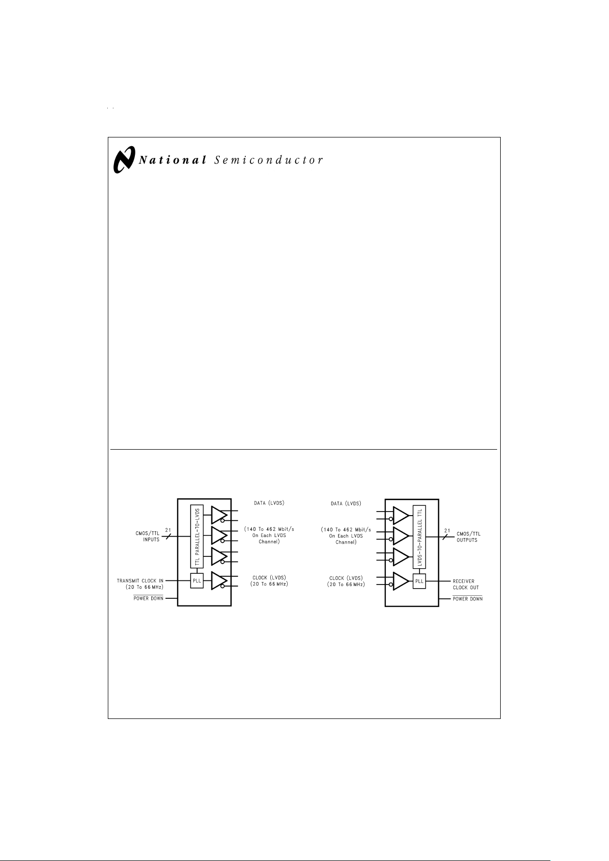
The DS90CR215 transmitter converts 21 bits of CMOS/TTL
data into three LVDS (Low Voltage Differential Signaling)
data streams.Aphase-locked transmit clockis transmitted in
parallel with thedata streams over a fourth LVDS link.Every
cycle of the transmit clock 21 bits of input data are sampled
and transmitted. The DS90CR216 receiver converts the
LVDS data streams back into 21 bits of CMOS/TTL data. At
a transmitclock frequencyof 66 MHz,21 bitsof TTLdata are
transmitted at a rate of 462 Mbps per LVDS data channel.
Using a 66 MHz clock, the data throughput is 1.386 Gbit/s
(173 Mbytes/s).
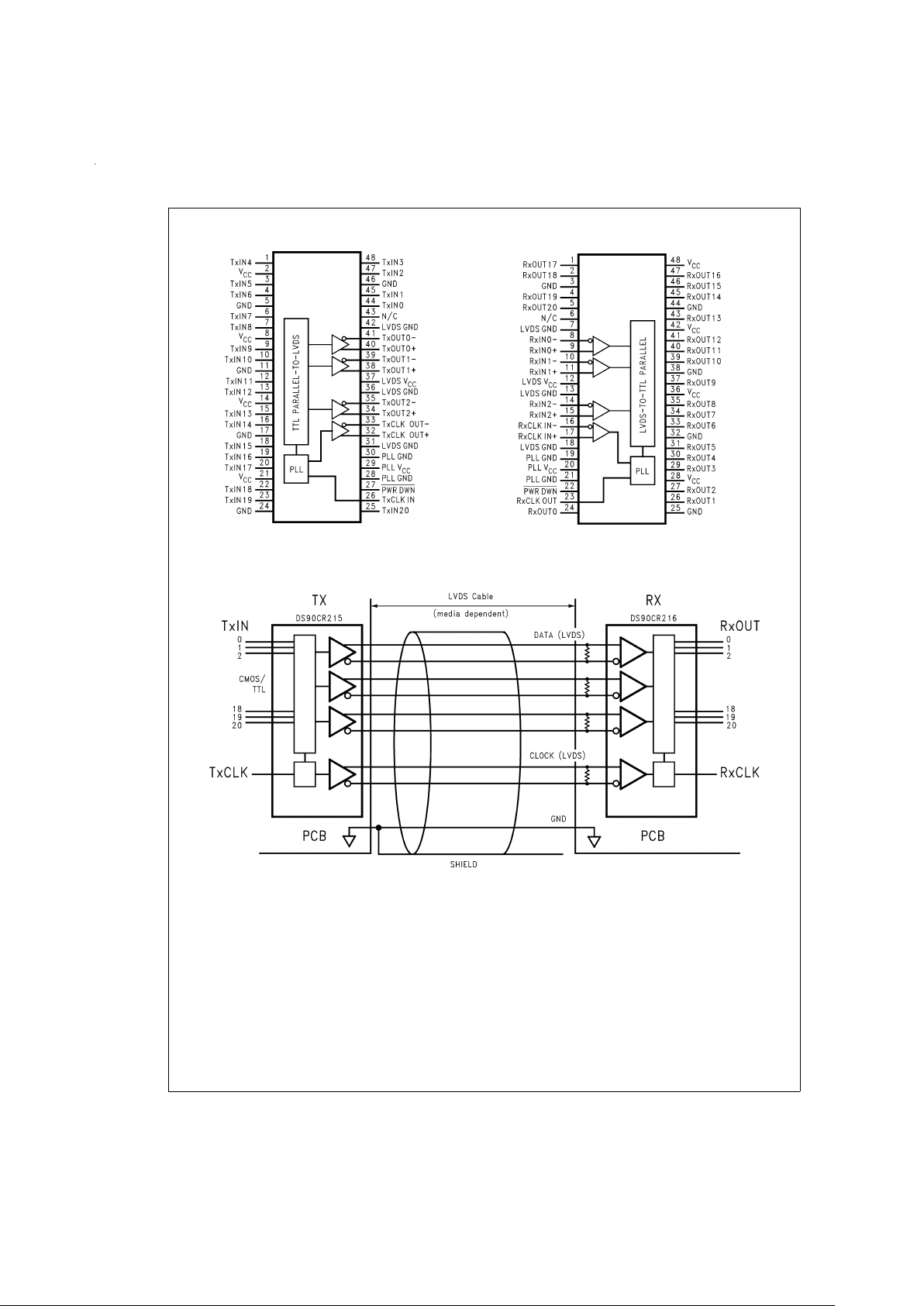
The multiplexing of the data lines provides a substantial
cable reduction. Long distance parallel single-ended buses
typically require a ground wire per active signal (and have
very limitednoise rejectioncapability). Thus,for a21-bit wide
data and one clock, up to 44 conductors are required. With
the Channel Link chipset as few as 9 conductors (3 data
pairs, 1 clock pair and a minimum of one ground) are
needed. This provides a 80%reduction in required cable
width, which provides a system cost savings, reduces connector physicalsize and cost,and reduces shieldingrequirements due to the cables’ smaller form factor.
The 21 CMOS/TTL inputs can support a variety of signal
combinations. For example, five 4-bit nibbles plus 1 control,
or two 9-bit (byte + parity) and 3 control.
Features
n Single +3.3V supply
n Chipset (Tx + Rx) power consumption
<
250 mW (typ)
n Power-down mode (
<
0.5 mW total)
n Up to 173 Megabytes/sec bandwidth
n Up to 1.386 Gbps data throughput
n Narrow bus reduces cable size
n 290 mV swing LVDS devices for low EMI
n +1V common mode range (around +1.2V)
n PLL requires no external components
n Low profile 48-lead TSSOP package
n Rising edge data strobe
n Compatible with TIA/EIA-644 LVDS standard
n ESD Rating
>
7kV
n Operating Temperature: −40˚C to +85˚C
Block Diagrams
TRI-STATE®is a registered trademark of National Semiconductor Corporation.
DS90CR215
DS012909-1
Order Number DS90CR215MTD
See NS Package Number MTD48
DS90CR216
DS012909-27
Order Number DS90CR216MTD
See NS Package Number MTD48
March 1999
DS90CR215/DS90CR216 +3.3V Rising Edge Data Strobe LVDS 21-Bit Channel Link-66 MHz
© 1999 National Semiconductor Corporation DS012909 www.national.com
Pin Diagrams
Typical Application
DS012909-21
DS90CR215
DS012909-22
DS90CR216
DS012909-23
www.national.com 2
Absolute Maximum Ratings (Note 1)
If Military/Aerospace specified devices are required,
please contactthe National Semiconductor Sales Office/
Distributors for availability and specifications.
Supply Voltage (V
CC
) −0.3V to +4V
CMOS/TTL Input Voltage −0.3V to (V
CC
+ 0.3V)
CMOS/TTL Output Voltage −0.3V to (V
CC
+ 0.3V)
LVDS Receiver Input Voltage −0.3V to (V
CC
+ 0.3V)
LVDS Driver Output Voltage −0.3V to (V
CC
+ 0.3V)
LVDS Output Short
Circuit Duration Continuous
Junction Temperature +150˚C
Storage Temperature Range −65˚C to +150˚C
Lead Temperature
(Soldering, 4 sec.) +260˚C
Maximum Package Power Dissipation
@
+25˚C
MTD48 (TSSOP) Package:
DS90CR215 1.98 W
DS90CR216 1.89 W
Package Derating
DS90CR215 16 mW/˚C above +25˚C
DS90CR216 15 mW/˚C above +25˚C
ESD Rating
(HBM, 1.5 kΩ, 100 pF)
>
7kV
Recommended Operating
Conditions
Min Nom Max Units
Supply Voltage (V
CC
) 3.0 3.3 3.6 V
Operating Free Air
Temperature (T
A
) −40 +25 +85 ˚C
Receiver Input Range 0 2.4 V
Supply Noise Voltage (V
CC
) 100 mV
PP
Electrical Characteristics
Over recommended operating supply and temperature ranges unless otherwise specified
Symbol Parameter Conditions Min Typ Max Units
CMOS/TTL DC SPECIFICATIONS
V
IH
High Level Input Voltage 2.0 V
CC
V
V
IL
Low Level Input Voltage GND 0.8 V
V
OH
High Level Output Voltage IOH= −0.4 mA 2.7 3.3 V
V
OL
Low Level Output Voltage IOL= 2 mA 0.06 0.3 V
V
CL
Input Clamp Voltage ICL= −18 mA −0.79 −1.5 V
I
IN
Input Current VIN=VCC, GND,
±
5.1
±
10 µA
2.5V or 0.4V
I
OS
Output Short Circuit Current V
OUT
= 0V -60 −120 mA
LVDS DRIVER DC SPECIFICATIONS
V
OD
Differential Output Voltage RL= 100Ω 250 290 450 mV
∆V
OD
Change in VODbetween
Complimentary Output States
35 mV
V
OS
Offset Voltage (Note 4) 1.125 1.25 1.375 V
∆V
OS
Change in VOSbetween
Complimentary Output States
35 mV
I
OS
Output Short Circuit Current V
OUT
= 0V, −3.5 −5 mA
R
L
= 100Ω
I
OZ
Output TRI-STATE®Current PWR DWN = 0V,
±
1
±
10 µA
V
OUT
=0VorV
CC
LVDS RECEIVER DC SPECIFICATIONS
V
TH
Differential Input High Threshold VCM= +1.2V +100 mV
V
TL
Differential Input Low Threshold −100 mV
I
IN
Input Current VIN= +2.4V, VCC= 3.6V
±
10 µA
V
IN
= 0V, VCC= 3.6V
±
10 µA
www.national.com3
Electrical Characteristics (Continued)
Over recommended operating supply and temperature ranges unless otherwise specified
Symbol Parameter Conditions Min Typ Max Units
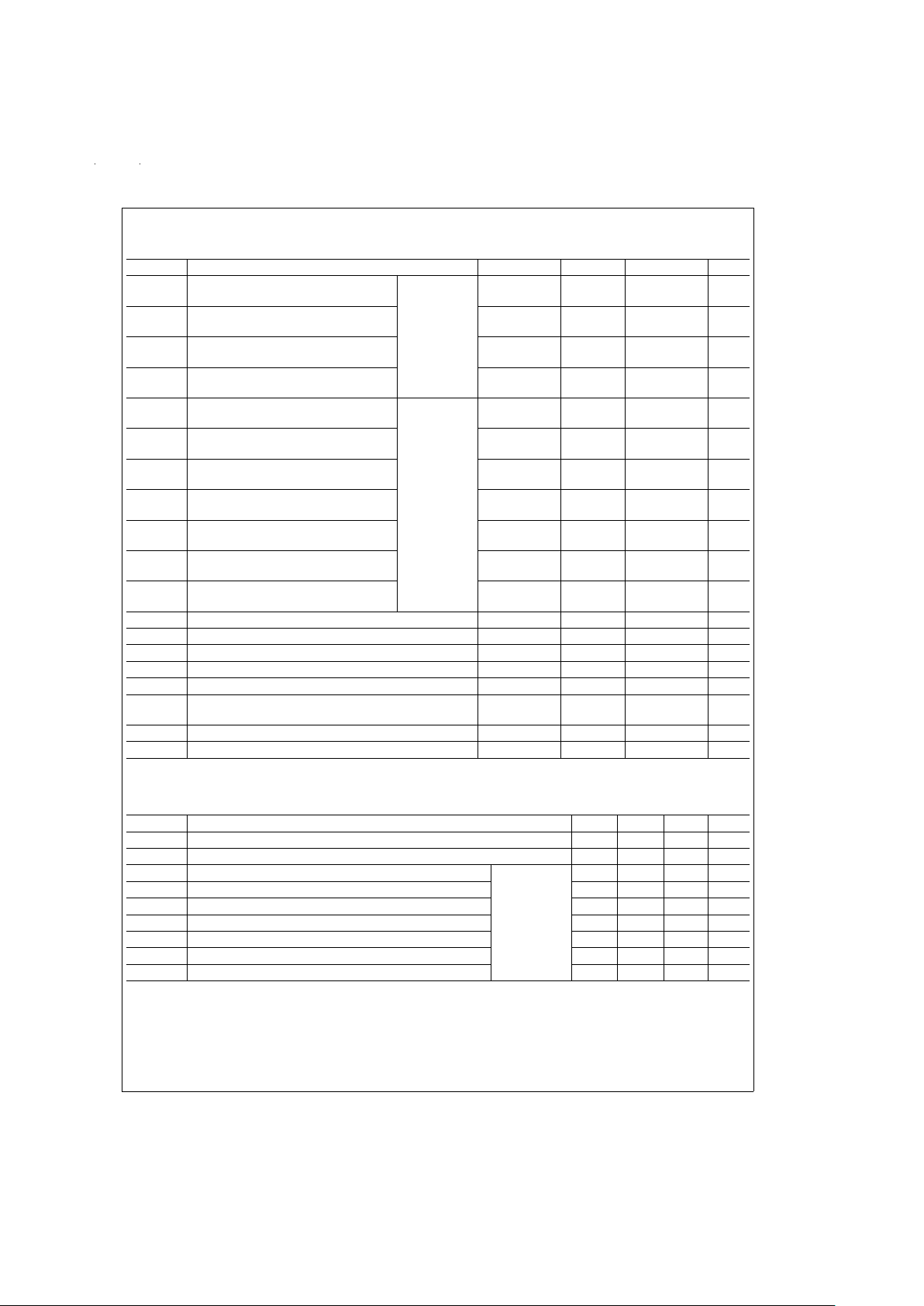
TRANSMITTER SUPPLY CURRENT
I
CCTW
Transmitter Supply Current
Worst Case (with Loads)
RL= 100Ω,
C
L
= 5 pF,
Worst Case
Pattern
(
Figures 1, 2
),
T
A
= −10˚C to
+70˚C
f = 32.5 MHz 31 45 mA
f = 37.5 MHz 32 50 mA
f = 66 MHz 37 55 mA
R
L
= 100Ω,
C
L
= 5 pF,
Worst Case
Pattern
(
Figures 1, 2
),
T
A
= −40˚C to
+85˚C
f = 40 MHz 38 51 mA
f = 66 MHz 42 55 mA
I
CCTZ
Transmitter Supply Current
Power Down
PWR DWN = Low
Driver Outputs in TRI-STATE
under Powerdown Mode
10 55 µA
RECEIVER SUPPLY CURRENT
I
CCRW
Receiver Supply Current Worst
Case
CL= 8 pF,
Worst Case
Pattern
(
Figures 1, 3
),
T
A
= −10˚C to
+70˚C
f = 32.5 MHz 49 65 mA
f = 37.5 MHz 53 70 mA
f = 66 MHz 78 105 mA
C
L
= 8 pF,
Worst Case
Pattern
(
Figures 1, 3
),
T
A
= −40˚C to
+85˚C
f = 40 MHz 55 82 mA
f = 66 MHz 78 105 mA
I
CCRZ
Receiver Supply Current Power
Down
PWR DWN = Low
Receiver Outputs Stay Low during
Powerdown Mode
10 55 µA
Note 1: “Absolute Maximum Ratings” are those values beyond which the safety of the device cannot be guaranteed. They are not meant to imply that the device
should be operated at these limits. The tables of “Electrical Characteristics” specify conditions for device operation.
Note 2: Typical values are given for V
CC
= 3.3V and TA= +25˚C.
Note 3: Current into device pins is defined as positive. Current out of device pins is defined as negative. Voltages arereferenced toground unlessotherwise specified (except V
OD
and ∆VOD).
Note 4: V
OS
previously referred as VCM.
Transmitter Switching Characteristics
Over recommended operating supply and −40˚C to +85˚C ranges unless otherwise specified
Symbol Parameter Min Typ Max Units
LLHT LVDS Low-to-High Transition Time (
Figure 2
) 0.5 1.5 ns
LHLT LVDS High-to-Low Transition Time (
Figure 2
) 0.5 1.5 ns
TCIT TxCLK IN Transition Time (
Figure 4
)5ns
TCCS TxOUT Channel-to-Channel Skew (
Figure 5
) 250 ps
TPPos0 Transmitter Output Pulse Position for
Bit0 (Note 7) (
Figure 16
)
f = 40 MHz −0.4 0 0.4 ns
TPPos1 Transmitter Output Pulse Position for
Bit1
3.1 3.3 4.0 ns
TPPos2 Transmitter Output Pulse Position for
Bit2
6.5 6.8 7.6 ns
www.national.com 4
Transmitter Switching Characteristics (Continued)
Over recommended operating supply and −40˚C to +85˚C ranges unless otherwise specified
Symbol Parameter Min Typ Max Units
TPPos3 Transmitter Output Pulse Position for
Bit3
10.2 10.4 11.0 ns
TPPos4 Transmitter Output Pulse Position for
Bit4
13.7 13.9 14.6 ns
TPPos5 Transmitter Output Pulse Position for
Bit5
17.3 17.6 18.2 ns
TPPos6 Transmitter Output Pulse Position for
Bit6
21.0 21.2 21.8 ns
TPPos0 Transmitter Output Pulse Position for
Bit0 (Note 6) (
Figure 16
)
f = 66 MHz −0.4 0 0.3 ns
TPPos1 Transmitter Output Pulse Position for
Bit1
1.8 2.2 2.5 ns
TPPos2 Transmitter Output Pulse Position for
Bit2
4.0 4.4 4.7 ns
TPPos3 Transmitter Output Pulse Position for
Bit3
6.2 6.6 6.9 ns
TPPos4 Transmitter Output Pulse Position for
Bit4
8.4 8.8 9.1 ns
TPPos5 Transmitter Output Pulse Position for
Bit5
10.6 11.0 11.3 ns
TPPos6 Transmitter Output Pulse Position for
Bit6
12.8 13.2 13.5 ns
TCIP TxCLK IN Period (
Figure 6
) 15 T 50 ns
TCIH TxCLK IN High Time (
Figure 6
) 0.35T 0.5T 0.65T ns
TCIL TxCLK IN Low Time (
Figure 6
) 0.35T 0.5T 0.65T ns
TSTC TxIN Setup to TxCLK IN (
Figure 6
) 2.5 ns
THTC TxIN Hold to TxCLK IN (
Figure 6
)0 ns
TCCD TxCLK IN to TxCLK OUT Delay
@
25˚C,VCC=3.3V
(
Figure 8
)
3 3.7 5.5 ns
TPLLS Transmitter Phase Lock Loop Set (
Figure 10
)10ms
TPDD Transmitter Powerdown Delay (
Figure 14
) 100 ns
Receiver Switching Characteristics
Over recommended operating supply and −40˚C to +85˚C ranges unless otherwise specified
Symbol Parameter Min Typ Max Units
CLHT CMOS/TTL Low-to-High Transition Time (
Figure 3
) 2.2 5.0 ns
CHLT CMOS/TTL High-to-Low Transition Time (
Figure 3
) 2.2 5.0 ns
RSPos0 Receiver Input Strobe Position for Bit 0 (Note 7)(
Figure 17
) f = 40 MHz 1.0 1.4 2.15 ns
RSPos1 Receiver Input Strobe Position for Bit 1 4.5 5.0 5.8 ns
RSPos2 Receiver Input Strobe Position for Bit 2 8.1 8.5 9.15 ns
RSPos3 Receiver Input Strobe Position for Bit 3 11.6 11.9 12.6 ns
RSPos4 Receiver Input Strobe Position for Bit 4 15.1 15.6 16.3 ns
RSPos5 Receiver Input Strobe Position for Bit 5 18.8 19.2 19.9 ns
RSPos6 Receiver Input Strobe Position for Bit 6 22.5 22.9 23.6 ns
www.national.com5
 Loading...