

NSC DS90CP04TLQX, DS90CP04TLQ Datasheet
DS90CP04
4x4 Low Power 2.5 Gb/s LVDS Digital Cross-Point
Switch
General Description
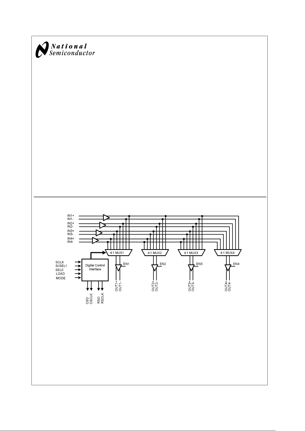
DS90CP04 is a 4x4 digital cross-point switch with broadside
input and output pins for efficient board layout. It utilizes Low
Voltage Differential Swing (LVDS) technology for low power,
high-speed operation. Data paths are fully differential from
input to output for low noise. The non-blocking architecture
allows connections of any input to any output or outputs. The
switch matrix consists of four differential 4:1 multiplexes.
Each output channel connects to one of the four inputs
common to all multiplexers. Each DS90CP04 output pair is
capable of independent operation up to 2.5Gb/s.
A simple serial control interface or a configuration select port
is activated by the state of the MODE pin. When utilizing the
serial control interface a single load command will update
the new switch configuration for all outputs simultaneously.
When the direct configuration port is used, output configurations are updated immediately based on the decoded
SEL0/1 logic state.
Features
n 2.5 Gbps fully differential data paths
n Non-blocking architecture
n Broadcast from any input
n Broadside pin-out
n Possible expansion to larger switch array
n Accepts LVDS/BLVDS/LVPECL/2.5V-CML inputs
n TRI-STATE LVDS outputs
n Serial control interface with read-back capability
n Double register loading
n Single +2.5V supply
n Low power, 575 mW Typ at 2.5 Gb/s
n Lead-less LLP-32 package 6x6 mm body size)
n Fabricated with advanced CMOS process technology
Functional Block Diagrams
20028701
April 2003
DS90CP04 4x4 Low Power 2.5 Gb/s LVDS Digital Cross-Point Switch
© 2003 National Semiconductor Corporation DS200287 www.national.com
Functional Block Diagrams (Continued)
20028702
DS90CP04
www.national.com 2
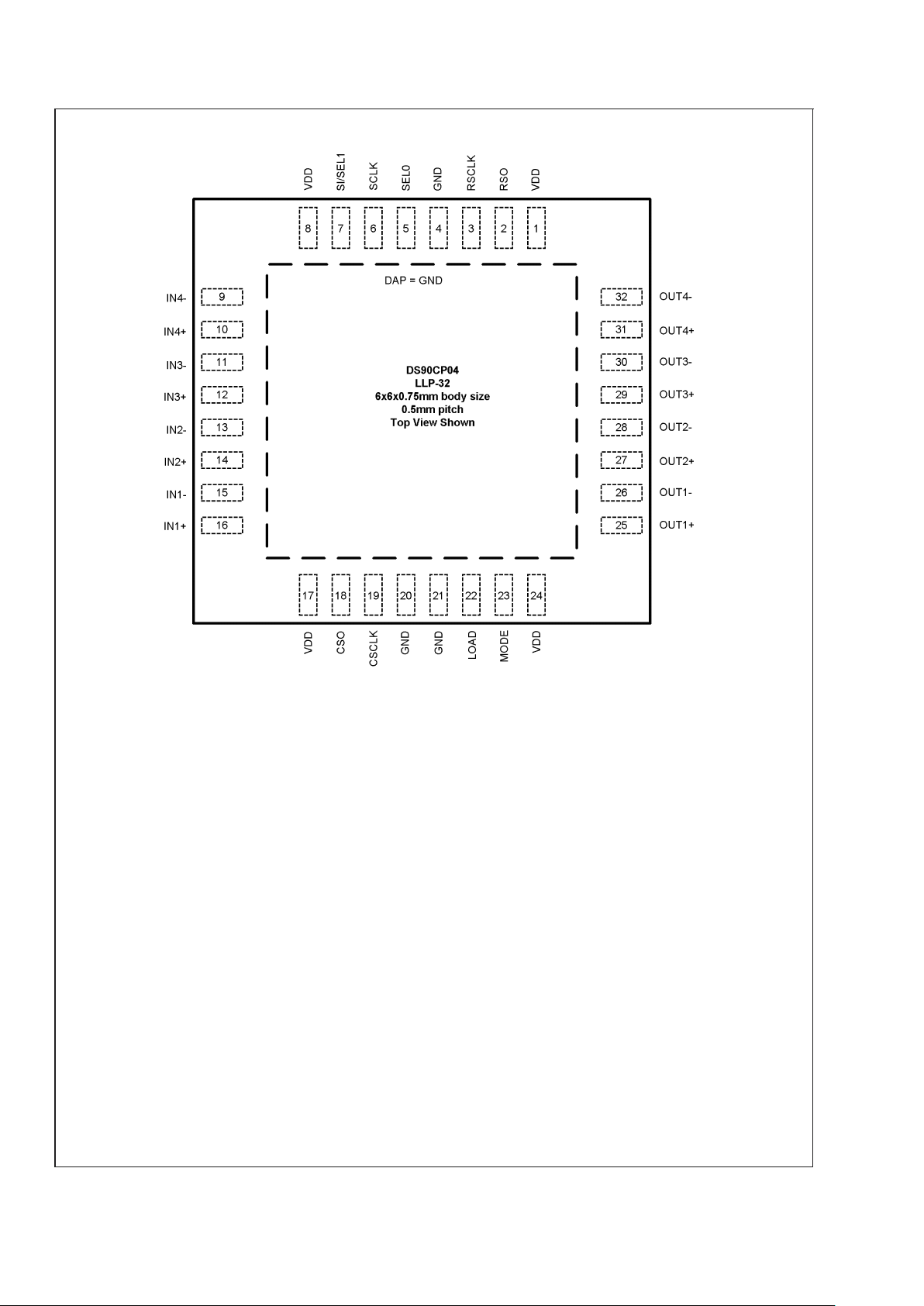
Connection Diagram
20028703
Order Number DS90CP04TLQ, DS90CP04TLQX (Tape and Reel)
See NS Package Number LQA32A
DS90CP04
www.national.com3
Pin Descriptions
Pin
Name
Pin
Number
I/O, Type Description
DIFFERENTIAL INPUTS COMMON TO ALL MUXES
IN1+
IN1−
16
15
I, LVDS Inverting and non-inverting differential inputs.
IN2+
IN2−
14
13
I, LVDS Inverting and non-inverting differential inputs.
IN3+
IN3−
12
11
I, LVDS Inverting and non-inverting differential inputs.
IN4+
IN4−
10
9
I, LVDS Inverting and non-inverting differential inputs.
SWITCHED DIFFERENTIAL OUTPUTS
OUT1+
OUT1−
25
26
O, LVDS Inverting and non-inverting differential outputs. OUT1
±
can be connected to any
one pair IN1
±
, IN2±, IN3±,orIN4
±
OUT2+
OUT2−
27
28
O, LVDS Inverting and non-inverting differential outputs. OUT2±can be connected to any
one pair IN1
±
, IN2±, IN3±,orIN4
±
OUT3+
OUT3−
29
30
O, LVDS Inverting and non-inverting differential outputs. OUT3±can be connected to any
one pair IN1
±
, IN2±, IN3±,orIN4
OUT4+
OUT4−
31
32
O, LVDS Inverting and non-inverting differential outputs. OUT4
±
can be connected to any
one pair IN1
±
, IN2±, IN3±,orIN4
±
DIGITAL CONTROL INTERFACE
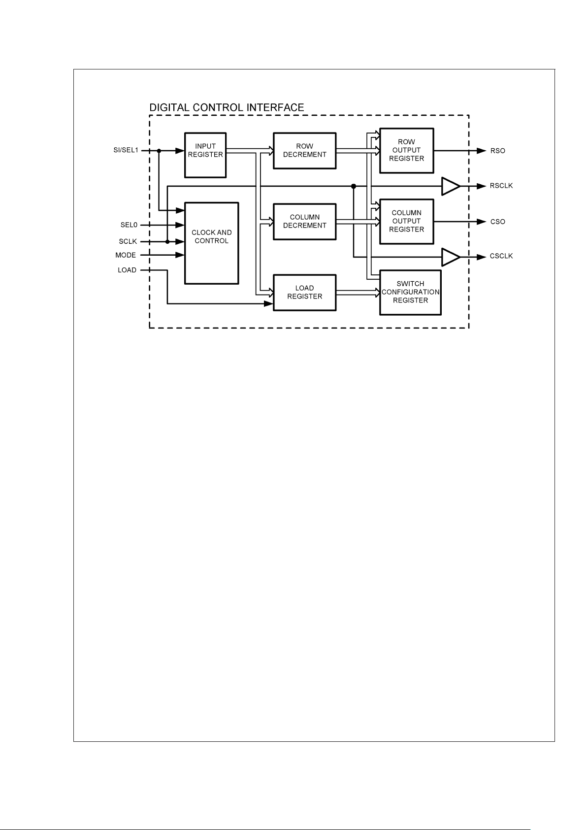
SCLK 6 I, LVCMOS Control clock to latch in programming data at SI. SCLK can be 0 MHz to
100 MHz. SCLK should be burst of clock pulses active only while accessing the
device. After completion of programming, SCLK should be kept at logic low to
minimize potential noise injection into the high-speed differential data paths.
SI / SEL1 7 I, LVCMOS Programming data to select the switch configuration. Data is latched into the input
buffer register at the rising edge of SCLK.
SEL0 5 I, LVCMOS Programming data to select the switch configuration.
CSO
RSO
18
2
O, LVCMOS With MODE low, control data is shifted out at CSO (RSO) for cascading to the
next device in the serial chain. The control data at CSO (RSO) is identical to that
shifted in at SI with the exception of the device column (row) address being
decremented by one internally before propagating to the next device in the chain.
CSO (RSO) is clocked out at the rising edge of SCLK.
CSCLK
RSCLK
19
3
O, LVCMOS With MODE low, these pins function as a buffered control clock from SCLK.
CSCLK (RSCLK) is used for cascading the serial control bus to the next device in
the serial chain.
LOAD 22 I, LVCMOS When LOAD is high and SCLK makes a LH transition, the device transfers the
programming data in the load register into the configuration registers. The new
switch configuration for all outputs takes effect. LOAD needs to remain high for
only one SCLK cycle to complete the process, holding LOAD high longer repeats
the transfer to the configuration register.
MODE 23 I, LVCMOS When MODE is low, the SCLK is active and a buffered SCLK signal is present at
the CLKOUT output. When MODE is high, the SCLK signal is uncoupled from
register and state machine internals. Internal registers will see an active low signal
until MODE is brought Low again.
POWER
V
DD
1, 8, 17,
24
I, Power VDD= 2.5V±5%. At least 4 low ESR 0.01 µF bypass capacitors should be
connected from V
DD
to GND plane.
GND 4, 20, 21,
DAP
I, Power Ground reference to LVDS and CMOS circuitry.
DAP is the exposed metal contact at the bottom of the LPP-32 package. The DAP
is used as the primary GND connection to the device. It should be connected to
the ground plane with at least 4 vias for optimal AC and thermal performance.
DS90CP04
www.national.com 4
Serial Interface Truth Table
LOAD MODE SCLK Resulting Action
0 0 LH The current state on SI is clocked into the input shift register.
0 1 LH Uncouples SCLK input from register and state machine internals. Internal registers
will see and the RSCLK and CSCLK outputs will drive an active Low signal until
MODE is brought Low again. See Configuration Select Truth Table below.
LH 0 X Loads OUT1– OUT4 configuration information from last valid frame. Places contents
of load register into the configuration register. The switch configuration is updated
asynchronously from the SCLK input.
1 1 LH Uncouples SCLK input from register and state machine internals. Internal registers
will see and the RSCLK and CSCLK outputs will drive an active Low signal until
MODE is brought Low again. See Configuration Select Truth Table below.
Configuration Select Truth Table
MODE SEL1 SEL0 Resulting Action
0 X X The SEL0/1 pins only function in configuration select mode. See below.
1 0 0 Distribution: IN1 - OUT1 OUT2 OUT3 OUT4
1 0 1 Distribution: IN2 - OUT1 OUT2 OUT3 OUT4
1 1 0 Redundancy: IN1 - OUT1 OUT2 and IN3 - OUT3 OUT4
1 1 1 Broadside: IN1 - OUT1, IN2 - OUT2, IN3 - OUT3, IN4 - OUT4
LH: Low to High (positive edge) transition.
X: Don’t Care or Not Applicable.
DS90CP04
www.national.com5
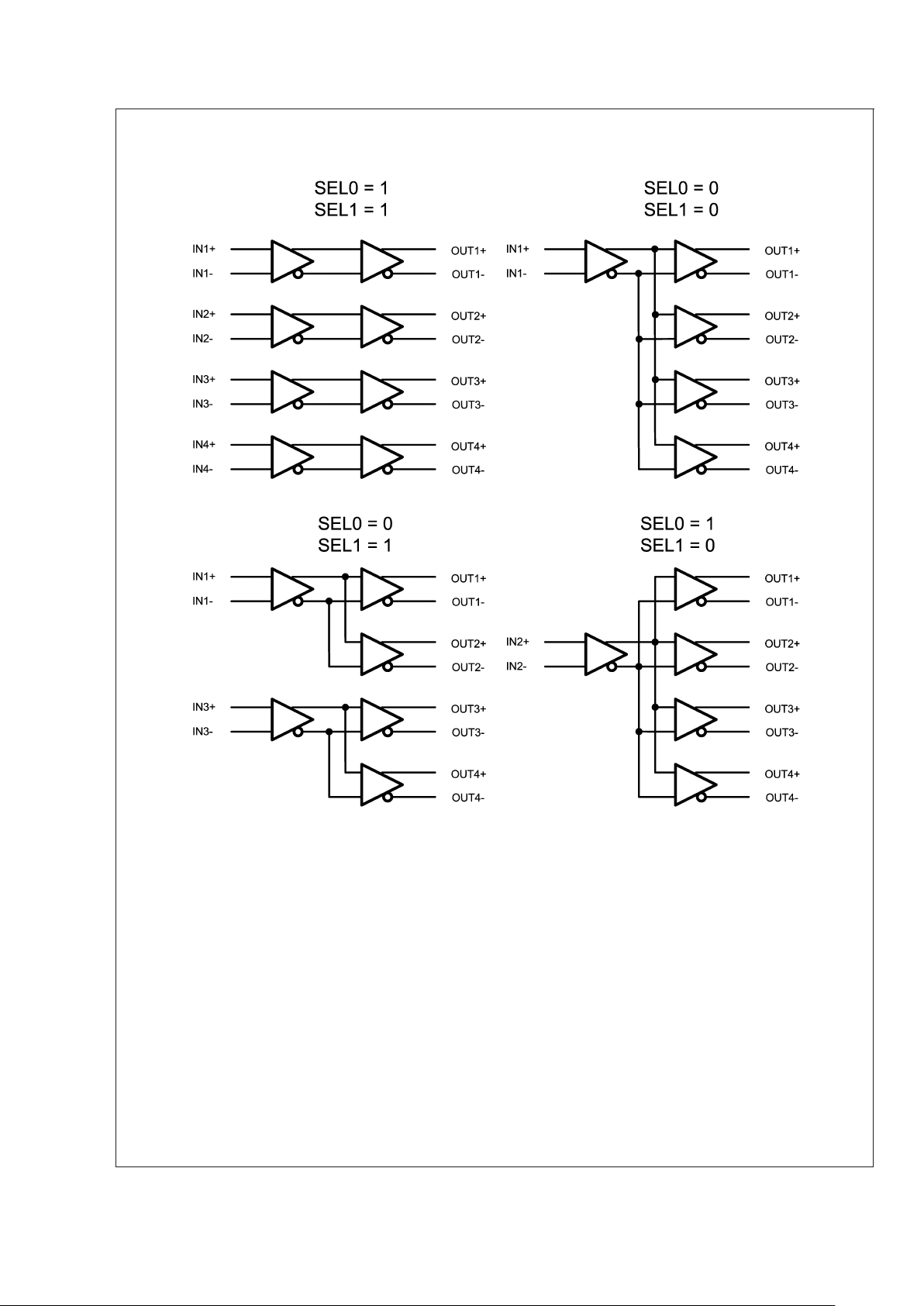
Configuration Select Truth Table (Continued)
20028704
FIGURE 1. DS90CP04 Configuration Select Decode
DS90CP04
www.national.com 6
 Loading...