

NSC DS90CF561MTDX, DS90CF561MTD Datasheet
DS90CF561/DS90CF562
LVDS 18-Bit Color Flat Panel Display (FPD) Link
General Description
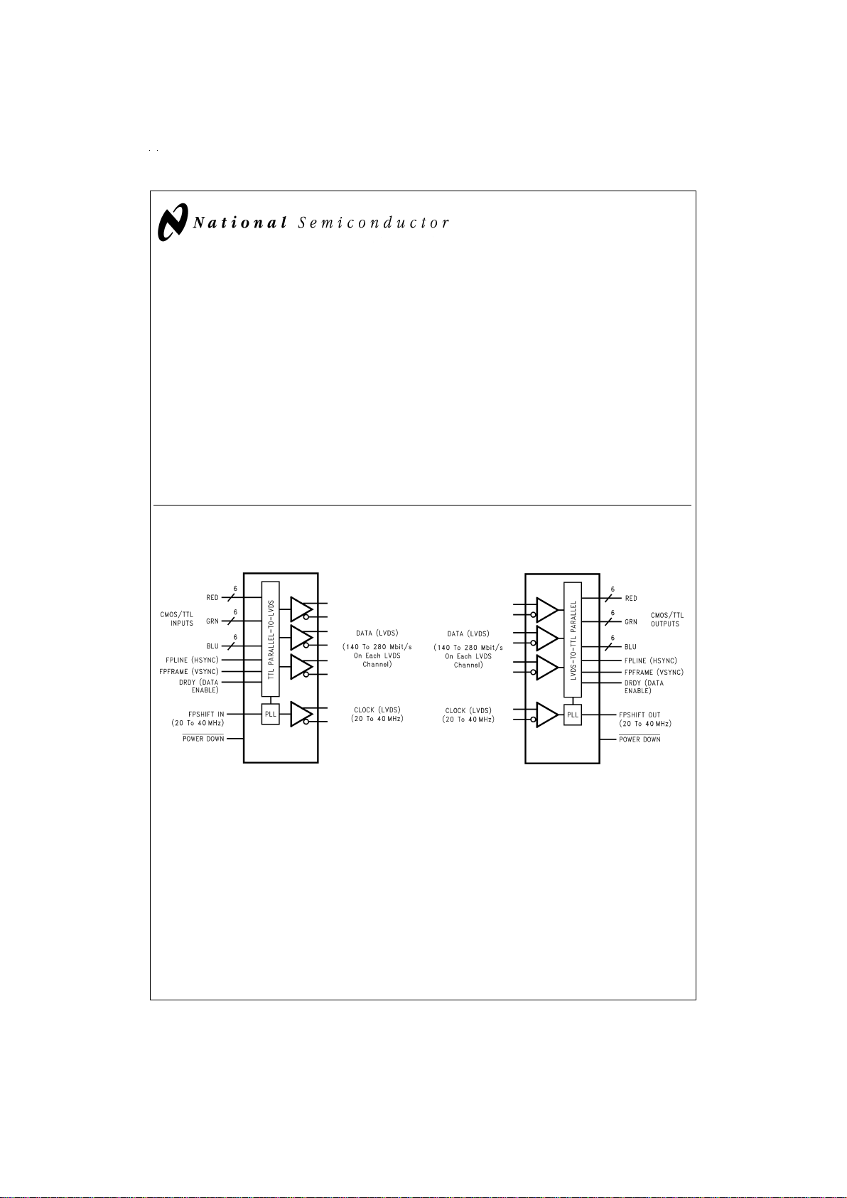
The DS90CF561 transmitter converts 21 bits of CMOS/TTL
data into three LVDS (Low Voltage Differential Signaling)
data streams.Aphase-locked transmit clockis transmitted in
parallel with the data streams over a fourth LVDS link. Every
cycle of the transmit clock 21 bits of input data are sampled
and transmitted. The DS90CF562 receiver converts the
LVDS data streams back into 21 bits of CMOS/TTL data. At
a transmit clock frequency of 40 MHz, 18 bits of RGB data
and 3 bits of LCD timing and control data (FPLINE, FPFRAME, DRDY) are transmitted at a rate of 280 Mbps per
LVDSdata channel. Using a 40 MHz clock, the data throughput is 105 Megabytes per second. These devices are offered
with falling edge data strobes for convenient interface with a
variety of graphics and LCD panel controllers.
This chipset is an ideal means to solve EMI and cable size
problems associated with wide, high speed TTL interfaces.
Features
n Up to 105 Megabyte/sec bandwidth
n Narrow bus reduces cable size and cost
n 290 mV swing LVDS devices for low EMI
n Low power CMOS design
n Power down mode
n PLL requires no external components
n Low profile 48-lead TSSOP package
n Falling edge data strobe
n Compatible with TIA/EIA-644 LVDS standard
Block Diagrams
TRI-STATE®is a registered trademark of National Semiconductor Corporation.
DS90CF561
DS012485-26
Order Number DS90CF561MTD
See NS Package Number MTD48
DS90CF562
DS012485-1
Order Number DS90CF562MTD
See NS Package Number MTD48
July 1997
DS90CF561/DS90CF562 LVDS 18-Bit Color Flat Panel Display (FPD) Link
© 1998 National Semiconductor Corporation DS012485 www.national.com
Block Diagrams (Continued)
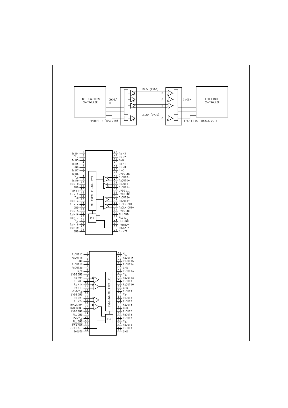
Connection Diagrams
Application
DS012485-2
DS90CF561
DS012485-3
DS90CF562
DS012485-4
www.national.com 2
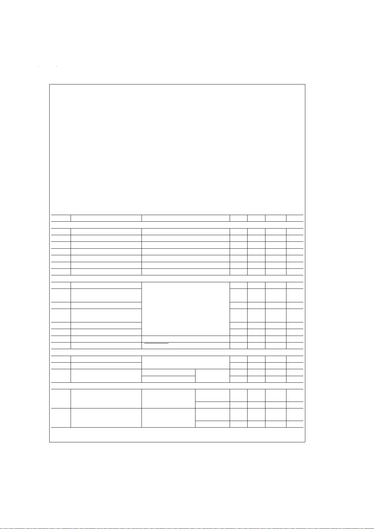
Absolute Maximum Ratings (Note 1)
If Military/Aerospace specified devices are required,
please contact the National Semiconductor Sales Office/
Distributors for availability and specifications.
Supply Voltage (V
CC
) −0.3V to +6V
CMOS/TTL Input Voltage −0.3V to (V
CC
+ 0.3V)
CMOS/TTL Ouput Voltage −0.3V to (V
CC
+ 0.3V)
LVDS Receiver Input Voltage −0.3V to (V
CC
+ 0.3V)
LVDS Driver Output Voltage −0.3V to (V
CC
+ 0.3V)
LVDS Output
Short Circuit Duration continuous
Junction Temperature +150˚C
Storage Temperature Range −65˚C to +150˚C
Lead Temperature
(Soldering, 4 sec.) +260˚C
Maximum Power Dissipation
@
+25˚C
MTD48 (TSSOP) Package:
DS90CF561 1.98W
DS90CF562 1.89W
Package Derating:
DS90CF561 16 mW/˚C above +25˚C
DS90CF562 15 mW/˚C above +25˚C
This device does not meet 2000V ESD rating (Note 4).
Recommended Operating
Conditions
Min Nom Max Units
Supply Voltage (V
CC
) 4.5 5.0 5.5 V
Operating Free Air
Temperature (T
A
) −10 +25 +70 ˚C
Receiver Input Range 0 2.4 V
Supply Noise Voltage (V
CC
) 100 mV
P-P
Electrical Characteristics
Over recommended operating supply and temperature ranges unless otherwise specified
Symbol Parameter Conditions Min Typ Max Units
CMOS/TTL DC SPECIFICATIONS
V
IH
High Level Input Voltage 2.0 V
CC
V
V
IL
Low Level Input Voltage GND 0.8 V
V
OH
High Level Output Voltage I
OH
=
−0.4 mA 3.8 4.9 V
V
OL
Low Level Output Voltage I
OL
=
2 mA 0.1 0.3 V
V
CL
Input Clamp Voltage I
CL
=
−18 mA −0.79 −1.5 V
I
IN
Input Current V
IN
=
V
CC
, GND, 2.5V or 0.4V
±
5.1
±
10 µA
I
OS
Output Short Circuit Current V
OUT
=
0V −120 mA
LVDS DRIVER DC SPEClFlCATIONS
V
OD
Differential Output Voltage R
L
=
100Ω 250 290 450 mV
∆V
OD
Change in VODbetween 35 mV
Complimentary Output States
V
CM
Common Mode Voltage 1.1 1.25 1.375 V
∆V
CM
Change in VCMbetween 35 mV
Complimentary Output States
V
OH
High Level Output Voltage 1.3 1.6 V
V
OL
Low Level Output Voltage 0.9 1.01 V
I
OS
Output Short Circuit Current V
OUT
=
0V, R
L
=
100Ω −2.9 −5 mA
I
OZ
Output TRI-STATE®Current Power Down=0V, V
OUT
=
0V or V
CC
±
1
±
10 µA
LVDS RECEIVER DC SPECIFlCATIONS
V
TH
Differential Input High Threshold V
CM
=
+1.2V +100 mV
V
TL
Differential Input Low Threshold −100 mV
I
IN
Input Current V
IN
=
+2.4V V
CC
=
5.5V
±
10 µA
V
IN
=
0V
±
10 µA
TRANSMITTER SUPPLY CURRENT
I
CCTW
Transmitter Supply Current,
Worst Case
R
L
=
100Ω,C
L
=
5 pF,
Worst Case Pattern
(
Figure 1,Figure 3
)
f=32.5 MHz 34 51 mA
f=37.5 MHz 36 53 mA
I
CCTG
Transmitter Supply Current,
16 Grayscale
R
L
=
100Ω,C
L
=
5 pF,
Grayscale Pattern
(
Figure 2,Figure 3
)
f=32.5 MHz 27 47 mA
f=37.5 MHz 28 48 mA
www.national.com3
Electrical Characteristics (Continued)
Over recommended operating supply and temperature ranges unless otherwise specified
Symbol Parameter Conditions Min Typ Max Units
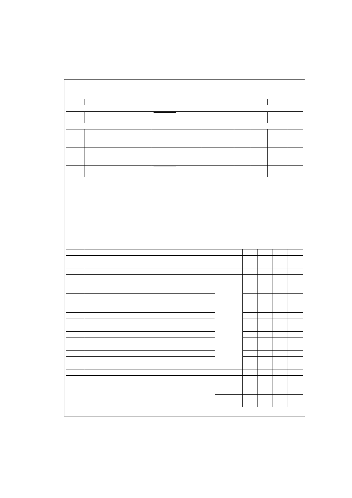
TRANSMITTER SUPPLY CURRENT
I
CCTZ
Transmitter Supply Current,
Power Down
Power Down=Low
125µA
RECEIVER SUPPLY CURRENT
I
CCRW
Receiver Supply Current,
Worst Case
C
L
=
8 pF,
Worst Case Pattern
(
Figure 1,Figure 4
)
f=32.5 MHz 55 75 mA
f=37.5 MHz 60 80 mA
I
CCRG
Receiver Supply Current,
16 Grayscale
C
L
=
8 pF,
16 Grayscale Pattern
(
Figure 2,Figure 4
)
f=32.5 MHz 35 55 mA
f=37.5 MHz 37 58 mA
I
CCRZ
Receiver Supply Current,
Power Down
Power Down=Low
110µA
Note 1: “Absolute Maximum Ratings” are those values beyond which the safety of the device cannot be guaranteed. They are not meant to imply that the device
should be operated at these limits. The tables of “Electrical Characteristics” specify conditions for device operation.
Note 2: Typical values are given for V
CC
=
5.0V and T
A
=
+25˚C.
Note 3: Current into device pins is defined as positive. Current out of device pins is defined as negative. Voltages are referenced to ground unless otherwise specified (except V
OD
and ∆VOD).
Note 4: ESD Rating:
HBM (1.5 kΩ, 100 pF)
PLL V
CC
≥ 1000V
All other pins ≥ 2000V
EIAJ (0Ω, 200 pF) ≥ 150V
Transmitter Switching Characteristics
Over recommended operating supply and temperature ranges unless otherwise specified
Symbol Parameter Min Typ Max Units
LLHT LVDS Low-to-High Transition Time (
Figure 3
) 0.75 1.5 ns
LHLT LVDS High-to-Low Transition Time (
Figure 3
) 0.75 1.5 ns
TCIT TxCLK IN Transition Time (
Figure 5
)8ns
TCCS TxOUT Channel-to-Channel Skew (Note 5) (
Figure 6
) 350 ps
TPPos0 Transmitter Output Pulse Position for Bit 0 (
Figure 17
)f
=
20 MHz −200 150 350 ps
TPPos1 Transmitter Output Pulse Position for Bit 1 6.3 7.2 7.5 ns
TPPos2 Transmitter Output Pulse Position for Bit 2 12.8 13.6 14.6 ns
TPPos3 Transmitter Output Pulse Position for Bit 3 20 20.8 21.5 ns
TPPos4 Transmitter Output Pulse Position for Bit 4 27.2 28 28.5 ns
TPPos5 Transmitter Output Pulse Position for Bit 5 34.5 35.2 35.6 ns
TPPos6 Transmitter Output Pulse Position for Bit 6 42.2 42.6 42.9 ns
TPPos0 Transmitter Output Pulse Position for Bit 0 (
Figure 16
)f
=
40 MHz −100 100 300 ps
TPPos1 Transmitter Output Pulse Position for Bit 1 2.9 3.3 3.9 ns
TPPos2 Transmitter Output Pulse Position for Bit 2 6.1 6.6 7.1 ns
TPPos3 Transmitter Output Pulse Position for Bit 3 9.7 10.2 10.7 ns
TPPos4 Transmitter Output Pulse Position for Bit 4 13 13.5 14.1 ns
TPPos5 Transmitter Output Pulse Position for Bit 5 17 17.4 17.8 ns
TPPos6 Transmitter Output Pulse Position for Bit 6 20.3 20.8 21.4 ns
TCIP TxCLK IN Period (
Figure 7
) 25 T 50 ns
TCIH TxCLK IN High Time (
Figure 7
) 0.35T 0.5T 0.65T ns
TCIL TxCLK IN Low Time (
Figure 7
) 0.35T 0.5T 0.65T ns
TSTC TxIN Setup to TxCLK IN (
Figure 7
)f
=
20 MHz 14 ns
f=40 MHz 8 ns
THTC TxIN Hold to TxCLK IN (
Figure 7
) 2.5 2 ns
www.national.com 4
 Loading...