

NSC DS75361N Datasheet
DS75361 Dual TTL-to-MOS Driver
DS75361 Dual TTL-to-MOS Driver
September 1992
General Description
The DS75361 is a monolithic integrated dual TTL-to-MOS
driver interface circuit. The device accepts standard TTL
input signals and provides high-current and high-voltage
output levels for driving MOS circuits. It is used to drive
address, control, and timing inputs for several types of MOS
RAMs including the 1103 and MM5270 and MM5280.
The DS75361 operates from standard TTL 5V supplies and
the MOS V
been optimized for operation with V
16V to 20V; however, it is designed for use over a much
wider range of V
supply in many applications. The device has
SS
.
CC2
supply voltage from
CC2
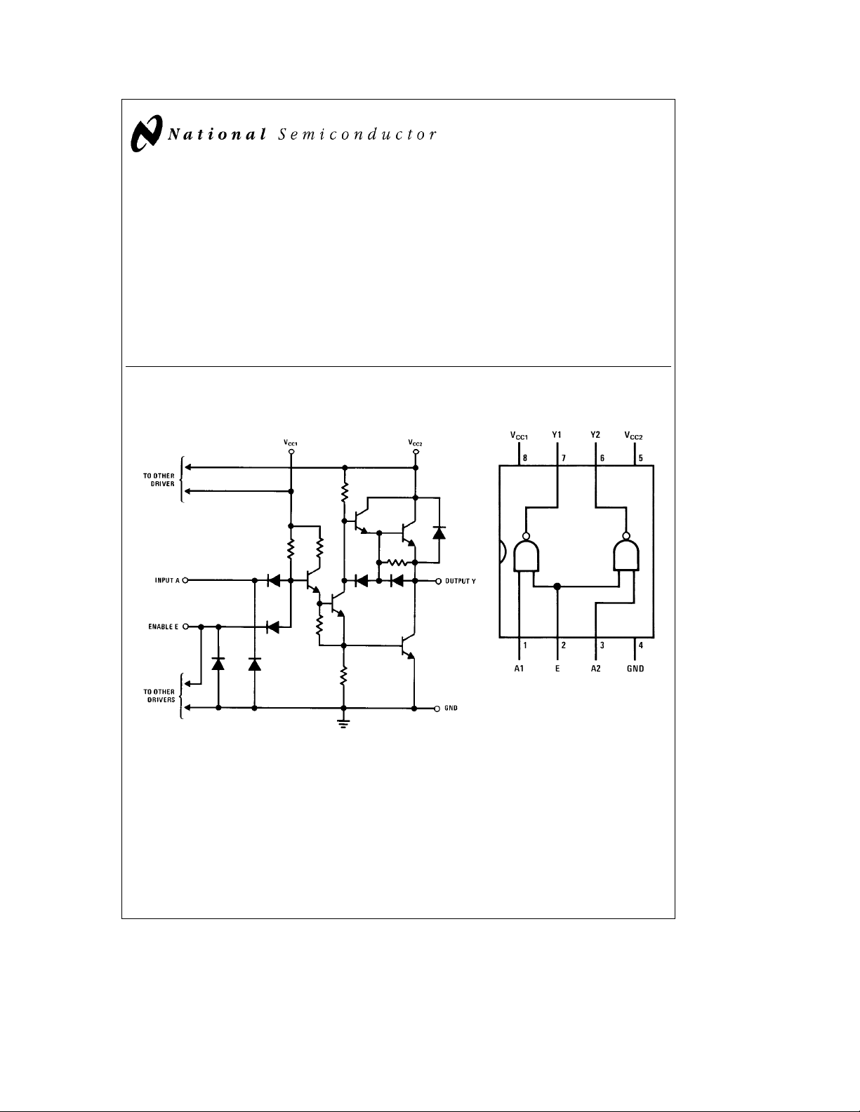
Schematic and Connection Diagrams
(1/2 shown)
Features
Y
Capable of driving high-capacitance loads
Y
Compatible with many popular MOS RAMs
Y
V
supply voltage variable over wide range to 24V
CC2
Y
Diode-clamped inputs
Y
TTL compatible
Y
Operates from standard bipolar and MOS supplies
Y
High-speed switching
Y
Transient overdrive minimizes power dissipation
Y
Low standby power dissipation
Dual-In-Line Package
Top View
TL/F/7557– 1
Order Number DS75361N
See NS Package Number N08E
TL/F/7557– 3
C
1995 National Semiconductor Corporation RRD-B30M105/Printed in U. S. A.
TL/F/7557
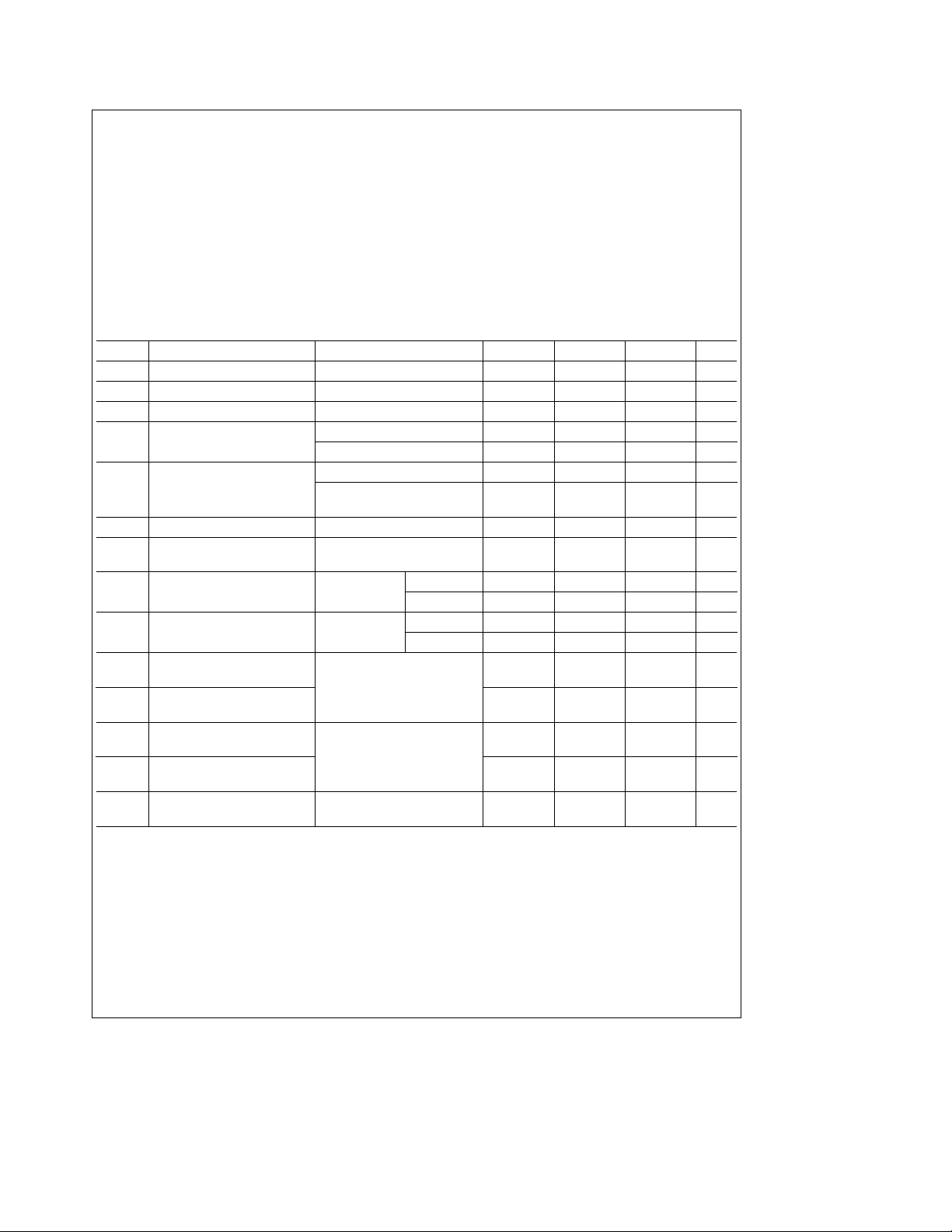
Absolute Maximum Ratings (Note 1)
If Military/Aerospace specified devices are required,
please contact the National Semiconductor Sales
Office/Distributors for availability and specifications.
Supply Voltage Range of V
Supply Voltage Range of V
CC1
CC2
(Note 1)
b
0.5 to 7V
b
0.5V to 25V
Input Voltage 5.5V
Inter-Input Voltage (Note 4) 5.5V
b
Storage Temperature Range
65§Ctoa150§C
Maximum Power Dissipation* at 25§C
Molded Package 1022 mW
Lead Temperature 1/16 inch from Case for
10 Seconds: N or P Package 200
*Derate molded package 8.2 mW/§above about 25§C.
Operating Conditions
Supply Voltage (V
Supply Voltage (V
) 4.75 5.25 V
CC1
) 4.75 24 V
CC2
Operating Temperature (TA)0
Min Max Units
a
70
C
§
C
§
Electrical Characteristics (Notes 2 and 3)
Symbol Parameter Conditions Min Typ Max Units
V
V
V
V
V
V
I
I
I
IH
I
IL
I
CC1(H)
I
CC2(H)
I
CC1(L)
I
CC2(L)
I
CC2(S)
High-Level Input Voltage 2 V
IH
Low-Level Input Voltage 0.8 V
IL
Input Clamp Voltage I
I
High-Level Output Voltage V
OH
Low-Level Output Voltage V
OL
Output Clamp Voltage V
O
Input Current at Maximum V
Input Voltage
High-Level Input Current
Low-Level Input Current
Supply Current from V
Outputs High
Supply Current from V
Outputs High
Supply Current from V
Outputs Low
Supply Current from V
Outputs Low
Supply Current from V
Stand-by Condition All Inputs at 5V, No Load
Note 1: ‘‘Absolute Maximum Ratings’’ are those values beyond which the safety of the device cannot be guaranteed. Except for ‘‘Operating Temperature Range’’
they are not meant to imply that the devices should be operated at these limits. The table of ‘‘Electrical Characteristics’’ provides conditions for actual device
operation.
Note 2: Unless otherwise specified min/max limits apply across the 0
e
20V.
V
CC2
Note 3: All currents into device pins shown as positive, out of device pins as negative, all voltages referenced to ground unless otherwise noted. All values shown
as max or min on absolute value basis.
Note 4: This rating applies between the A input of either driver and the common E input.
, Both
CC1
, Both
CC2
, Both
CC1
, Both
CC2
,V
CC2
eb
12 mA
I
e
0.8V, I
IL
e
V
0.8V, I
IL
e
2V, I
IH
e
V
CC2
e
I
40 mA
OL
e
0V, I
I
e
5.5V 1 mA
I
e
V
2.4V
I
e
V
0.4V
I
eb
50 mAV
OH
eb
10 mA V
OH
e
10 mA 0.15 0.3 V
OL
15V to 24V, V
e
OH
e
2V,
IH
20 mA V
CC2
CC2
b
1V
b
2.3 V
b
CC2
b
CC2
0.25 0.5 V
A Inputs 40 mA
E Input 80 mA
b
A Inputs
E Input
1
b
2
24mA
e
V
5.25V, V
CC1
All Inputs at 0V, No Load
CC2
e
24V,
16 24 mA
e
V
5.25V, V
CC1
All Inputs at 5V, No Load
e
0V, V
CC1
Ctoa70§C range for the DS75361. All typical values are for T
§
CC2
CC2
e
24V,
711mA
e
24V,
b
1.5 V
0.7 V
1.8 V
a
1.5 V
CC2
b
1.6 mA
b
3.2 mA
0.5 mA
0.5 mA
e
A
25§C and V
CC1
e
5V and
2
 Loading...