

NSC DS75161AN, DS75160AN Datasheet

DS75160A/DS75161A
IEEE-488 GPIB Transceivers
DS75160A/DS75161A IEEE-488 GPIB Transceivers
May 1999
General Description
This family of high-speed-Schottky 8-channel bi-directional
transceivers is designed to interface TTL/MOS logic to the
IEEE Standard 488-1978 General Purpose Interface Bus
(GPIB). PNP inputs are usedatalldriver inputs for minimum
loading, and hysteresis is provided at all receiver inputs for
added noise margin. The IEEE-488 required bus termination
is provided internally with an active turn-off feature which disconnects the termination from the bus when V
The General Purpose Interface Bus is comprised of 16 signal lines — 8 for data and 8 for interface management. The
data lines are always implemented with DS75160A, and the
management lines are either implemented with DS75161A in
a single-controller system.
is removed.
CC
Connection Diagrams
Dual-In-Line Package
Features
n 8-channel bi-directional non-inverting transceivers
n Bi-directional control implemented with TRI-STATE
output design
n Meets IEEE Standard 488-1978
n High-speed Schottky design
n Low power consumption
n High impedance PNP inputs (drivers)
n 500 mV (typ) input hysteresis (receivers)
n On-chip bus terminators
n No bus loading when V
n Pin selectable open collector mode on DS75160A driver
outputs
n Accommodates multi-controller systems
Dual-In-Line Package
Order Number DS75161AN or DS75161AWM
See NS Package Number M20B or N20B
is removed
CC
®
DS005804-16
DS005804-1
Order Number DS75160AN or DS75160AWM
See NS Package Number M20B or N20A
TRI-STATE®is a registered trademark of National Semiconductor Corporation.
© 1999 National Semiconductor Corporation DS005804 www.national.com
Top View
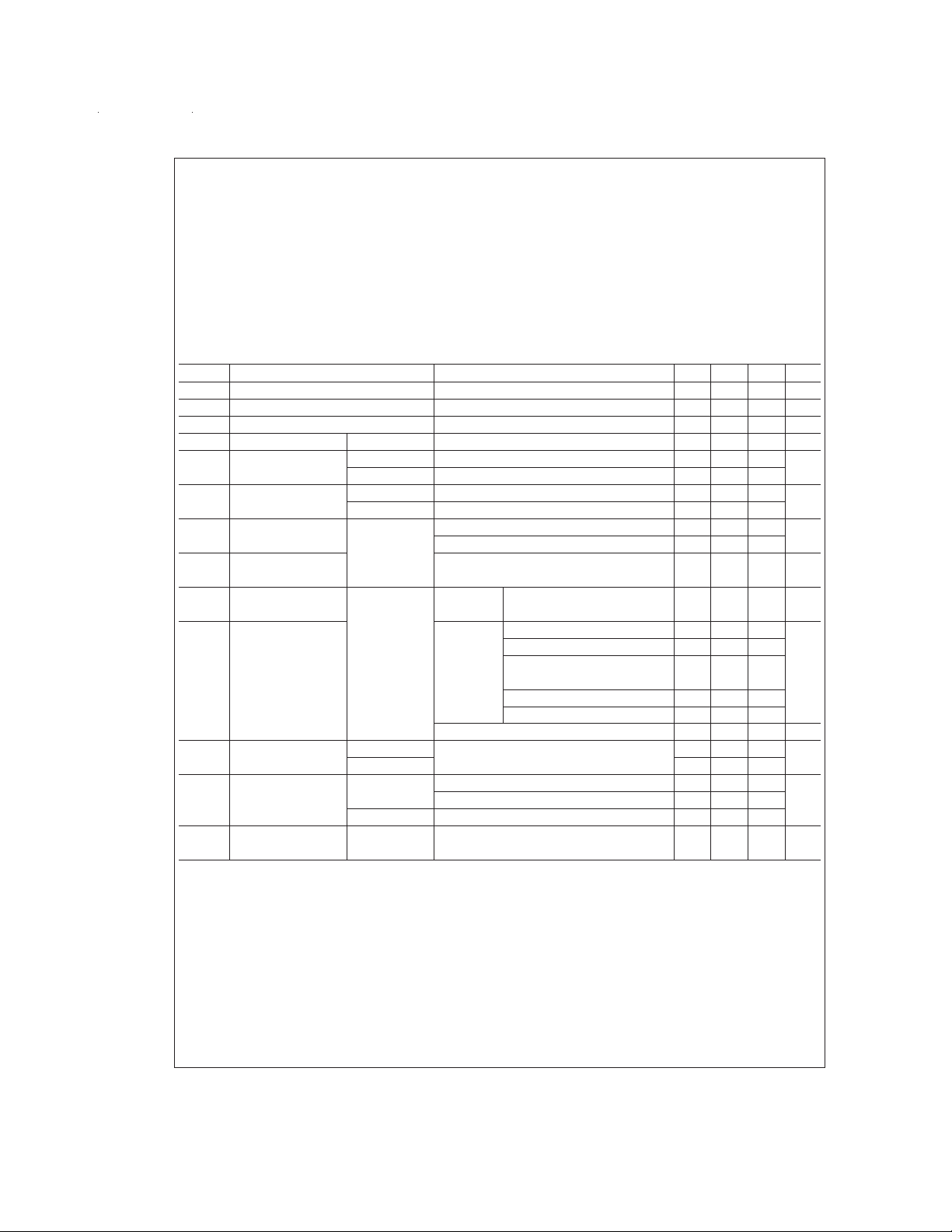
Absolute Maximum Ratings (Note 2)
If Military/Aerospace specified devices are required,
please contact the National Semiconductor Sales Office/
Distributors for availability and specifications.
Supply Voltage, V
CC
Input Voltage 5.5V
Storage Temperature Range −65˚C to +150˚C
Lead Temperature (Soldering, 4 sec.) 260˚C
7.0V
Molded Package 1897 mW
Min Max Units
, Supply Voltage 4.75 5.25 V
V
CC
, Ambient Temperature 0 70 ˚C
T
A
, Output Low Current
I
OL
Bus 48 mA
Terminal 16 mA
Note 1: Derate molded package 15.2 mW/˚C above 25˚C.
Maximum Power Dissipation (Note 1) at 25˚C
Electrical Characteristics (Notes 3, 4)
Symbol Parameter Conditions Min Typ Max Units
V
IH
V
IL
V
IK
V
HYS
V
OH
V
OL
I
IH
I
IL
V
BIAS
I
LOAD
I
OS
I
CC
C
IN
Note 2: “Absolute Maximum Ratings” are those values beyond which the safety of the device cannot be guaranteed. They are not meant to imply that the device
should be operated at these limits. The table of “Electrical Characteristics” provides conditions for actual device operation.
Note 3: Unless otherwise specified, min/max limits apply across the 0˚C to +70˚C temperature range and the 4.75V to 5.25V power supply range. All typical values
are for T
Note 4: All currents into device pins are shown as positive; all currents out of device pins are shown as negative; all voltages are referenced to ground, unless otherwise specified. All values shown as max or min are so classified on absolute value basis.
Note 5: Only one output at a time should be shorted.
Note 6: This characteristic does not apply to outputs on DS75161A that are open collector.
High-Level Input Voltage 2 V
Low-Level Input Voltage 0.8 V
Input Clamp Voltage I
=
−18 mA −0.8 −1.5 V
I
Input Hysteresis Bus 400 500 mV
High-Level Terminal I
Output Voltage Bus (Note 4) I
Low-Level Terminal I
Output Voltage Bus I
High-Level Terminal and V
Input Current TE, PE, DC, V
Low-Level SC Inputs V
=
−800 µA 2.7 3.5 V
OH
=
−5.2 mA 2.5 3.4
OH
=
16 mA 0.3 0.5 V
OL
=
48 mA 0.4 0.5
OH
=
5.5V 0.2 100 µA
I
=
2.7V 0.1 20
I
=
0.5V −10 −100 µA
I
Input Current
Terminator Bias Driver I
=
0 (No Load) 2.5 3.0 3.7 V
I(bus)
Voltage at Bus Port Disabled
Terminator V
Bus Loading V
Current Bus Driver V
=
−1.5V to 0.4V −1.3
I(bus)
=
0.4V to 2.5V 0 −3.2
I(bus)
=
2.5V to 3.7V 2.5 mA
I(bus)
Disabled −3.2
=
V
3.7V to 5V 0 2.5
I(bus)
=
V
5V to 5.5V 0.7 2.5
I(bus)
0V, V
=
0V to 2.5V 40 µA
I(bus)
=
0V (Note 5) −15 −35 −75 mA
O
Short-Circuit Terminal V
=
V
CC
=
2V, V
I
Output Current Bus (Note 6) −35 −75 −150
Supply Current DS75160A Transmit, TE=2V, PE=2V, V
Receive, TE=0.8V, PE=2V, V
DS75161A TE=0.8V, DC=0.8V, V
Bus-Port Bus V
=
CC
5V or 0V, V
=
0V to 2V, 20 30 pF
I
=
0.8V 85 125
I
=
0.8V 70 100 mA
I
=
0.8V 84 125
I
Capacitance f=1 MHz
=
A
25˚C and V
=
5.0V.
CC
www.national.com 2
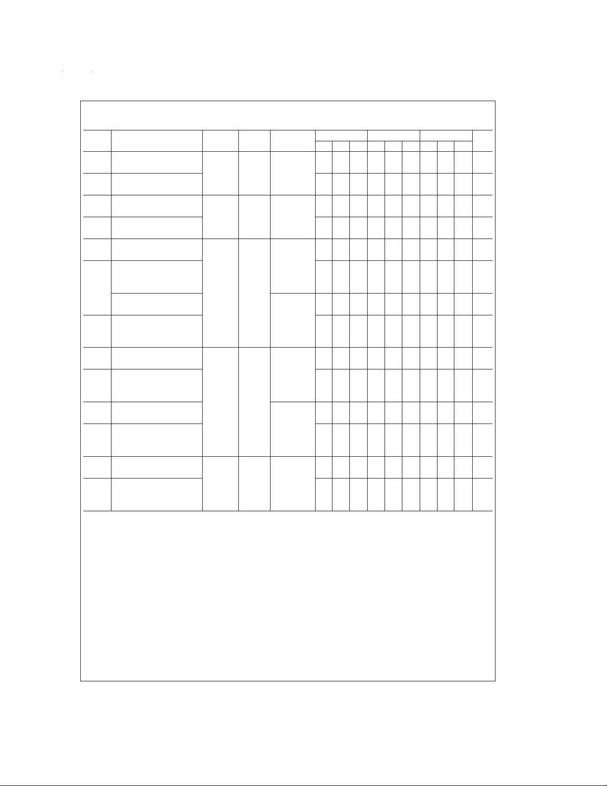
Switching Characteristics (Note 7)
=
V
5.0V
CC
Symbol Parameter From To Conditions DS75160A DS75161A DS75162A Units
Propagation Delay Time, V
t
PLH
Low to High Level Output Terminal Bus R
t
Propagation Delay Time, C
PHL
High to Low Level Output
t
Propagation Delay Time, V
PLH
Low to High Level Output Bus Terminal R
t
Propagation Delay Time, C
PHL
High to Low Level Output
t
Output Enable Time V
PZH
to High Level V
t
Output Disable Time TE, DC, R
PHZ
From High Level or SC C
t
Output Enable Time (Note 8) Bus V
PZL
to Low Level (Note 9) V
t
Output Disable Time R
PLZ
From Low Level C
t
Output Enable Time V
PZH
to High Level V
t
Output Disable Time TE, DC, R
PHZ
From High Level or SC Terminal C
t
Output Enable Time (Note 8) V
PZL
to Low Level (Note 9) V
t
Output Disable Time R
PLZ
From Low Level C
t
Output Pull-Up Enable V
PZH
Time (DS75160A Only) PE Bus V
t
Output Pull-Up Disable (Note 8) R
PHZ
Time (DS75160A Only) C
Note 7: Typical values are for V
Note 8: Refer to Functional Truth Tables for control input definition.
Note 9: Test configuration should be connected to only one transceiver at a time due to the high current stress caused by the V
nected to that input becomes active.
±
5%,T
=
0˚C to 70˚C
A
CC
=
5.0V and T
=
L
=
L
=
L
Figure 1
=
L
=
L
=
L
Figure 2
=
I
=
L
=
L
=
L
Figure 1
=
I
=
L
=
L
=
L
Figure 1
=
I
=
L
=
L
=
L
Figure 1
=
I
=
L
=
L
=
L
Figure 1
=
I
=
L
=
L
=
L
Figure 1
=
25˚C and are meant for reference only.
A
Min Typ Max Min Typ Max Min Typ Max
2.3V 10 20 10 20 10 20 ns
38.3Ω
30 pF 14 20 14 20 14 20 ns
5.0V 14 20 14 20 14 20 ns
240Ω
30 pF 10 20 10 20 10 20 ns
3.0V 19 32 23 40 23 40 ns
0V
480Ω 15 22 15 25 15 25 ns
15 pF
0V 24 35 28 48 28 48 ns
2.3V
38.3Ω 17 25 17 27 17 27 ns
15 pF
3.0V 17 33 18 40 18 40 ns
0V
3kΩ 15 25 22 33 22 33 ns
15 pF
0V 25 39 28 52 28 52 ns
5V
280Ω 15 27 20 35 20 35 ns
15 pF
3V 10 17 NA NA ns
0V
480Ω 10 15 NA NA ns
15 pF
voltage source when the output con-
I
www.national.com3
 Loading...