

NSC DS75154MX, DS75154M Datasheet
DS75154
Quad Line Receiver
General Description
The DS75154 is a quad monolithic line receiver designed to
satisfy the requirements of the standard interface between
data terminalequipment and data communication equipment
as defined by EIA Standard RS-232C. Other applications are
in relatively short, single-line, point-to-point data transmission systems and for level translators. Operation is normally
from a single 5V supply; however, a built-in option allows operation from a 12V supply without the use of additional components. The output is compatible with most TTL and LS circuits when either supply voltage is used.
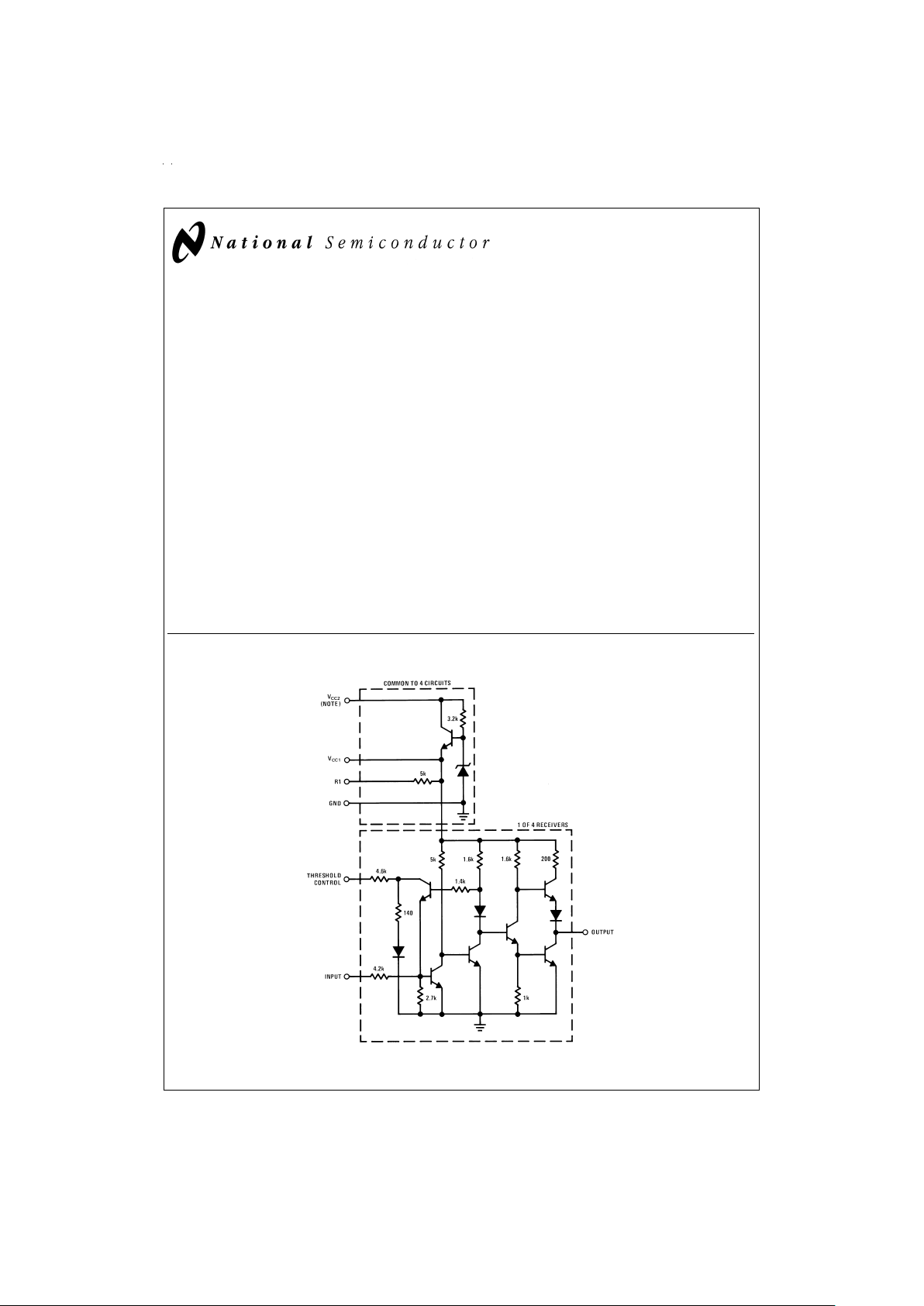
In normal operation, the threshold-control terminals are connected to the V
CC1
terminal, pin 15, even if power is being
supplied via the alternate V
CC2
terminal, pin 16. This provides a wide hysteresis loop which is the difference between
the positive-going and negative-going threshold voltages. In
this mode, if the input voltage goes to zero, the output voltage will remain at the low or high level as determined by the
previous input.
For fail-safe operation, the threshold-control terminals are
open. This reduces the hysteresis loop by causing the
negative-going threshold voltage to be above zero. The
positive-going threshold voltage remains above zero as it is
unaffected by the disposition of the threshold terminals. In
the fail-safe mode, if the input voltage goes to zero or an
open-circuit condition, the output will go to the high level regardless of the previous input condition.
Features
n Input resistance, 3 kΩ to7kΩover full RS-232C voltage
range
n Input threshold adjustable to meet “fail-safe”
requirements without using external components
n Inverting output compatible with TTL or LS
n Built-in hysteresis for increased noise immunity
n Output with active pull-up for symmetrical switching
speeds
n Standard supply voltage—5V or 12V
Schematic Diagram
DS005795-1
Note: When using V
CC1
(pin 15), V
CC2
(pin 16) may be left open or shorted to V
CC1
. When using V
CC2,VCC1
must be left open or connected to the
threshold control pins.
May 1998
DS75154 Quad Line Receiver
© 1998 National Semiconductor Corporation DS005795 www.national.com
Absolute Maximum Ratings (Note 2)
If Military/Aerospace specified devices are required,
please contact the National Semiconductor Sales Office/
Distributors for availability and specifications.
Normal Supply Voltage (Pin 15),
(V
CC1
)7V
Alternate Supply Voltage (Pin 16),
(V
CC2
) 14V
Input Voltage
±
25V
Storage Temperature Range −65˚C to +150˚C
Maximum Power Dissipation (Note 1) at 25˚C
SO Package 650 mW
Lead Temperature (Soldering, 4
seconds) 260˚C
Operating Conditions
Min Max Units
Supply Voltage (Pin 15), (V
CC1
) 4.5 5.5 V
Alternate Supply Voltage
(Pin 16), (V
CC2
) 10.8 13.2 V
Input Voltage
±
15 V
Temperature, (T
A
) 0 +70 ˚C
Note 1: Derate molded DIP package 10.9 mW/˚C above 25˚C; derate SO
package 8.01 mW/˚C above 25˚C.
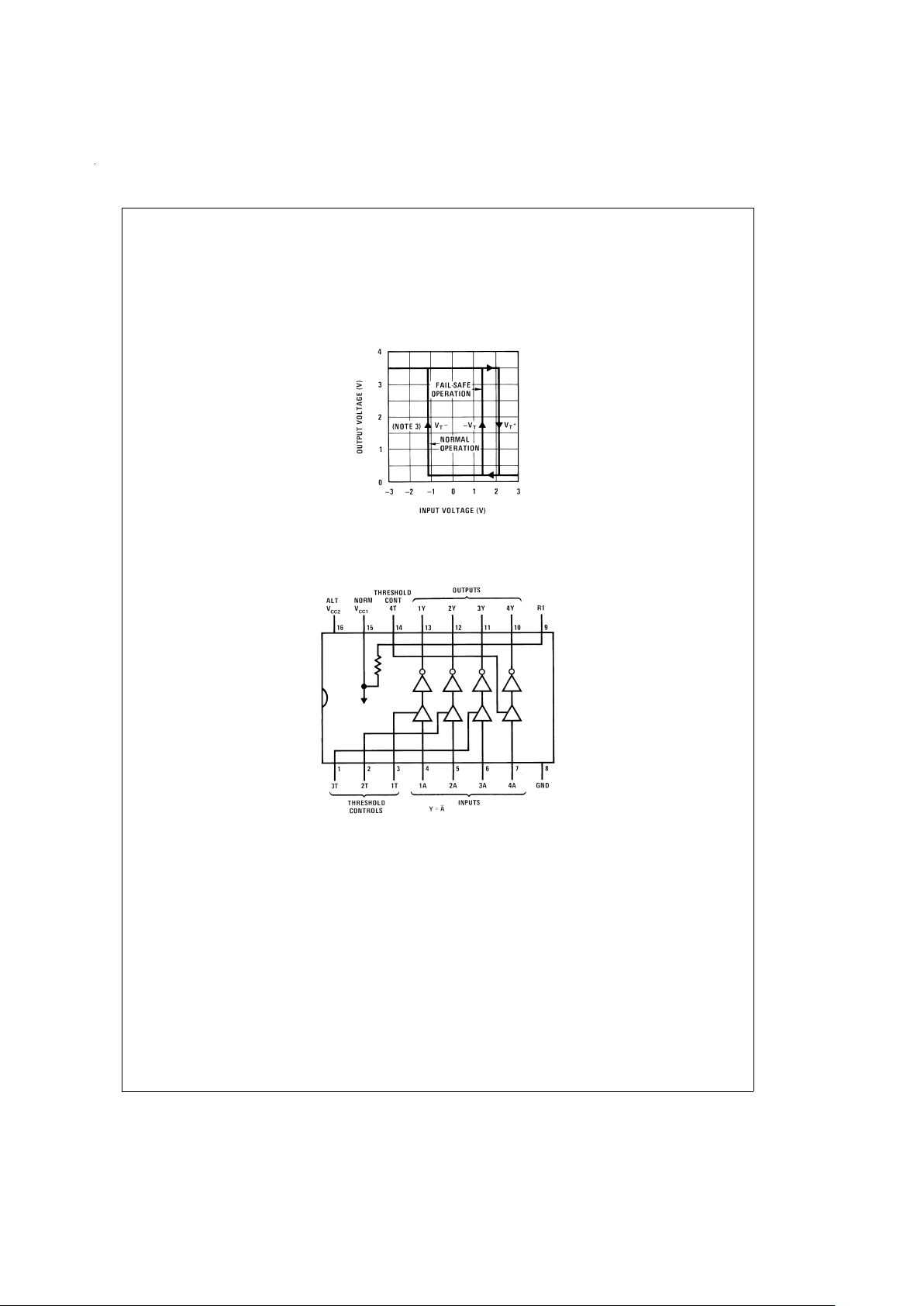
Electrical Characteristics (Notes 3, 4, 5)
Symbol Parameter Conditions Min Typ Max Units
V
IH
High-Level Input Voltage (
Figure 1
)3V
V
IL
Low-Level Input Voltage (
Figure 1
)−3V
V
T+
Positive-Going Threshold Voltage (
Figure 1
) Normal Operation 0.8 2.2 3 V
Fail-Safe Operation 0.8 2.2 3 V
V
T−
Negative-Going Threshold Voltage (
Figure 1
) Normal Operation −3 −1.1 0 V
Fail-Safe Operation 0.8 1.4 3 V
V
T+−VT−
Hysteresis (
Figure 1
) Normal Operation 0.8 3.3 6 V
Fail-Safe Operation 0 0.8 2.2 V
V
OH
High-Level Output Voltage I
OH
=
−400 µA, (
Figure 1
) 2.4 3.5 V
V
OL
Low-Level Output Voltage I
OL
=
16 mA, (
Figure 1
) 0.23 0.4 V
r
I
Input Resistance (
Figure 2
) ∆V
I
=
−25V to −14V 3 5 7 kΩ
∆V
I
=
−14V to −3V 3 5 7 kΩ
∆V
I
=
−3V to +3V 3 6 kΩ
∆V
I
=
3V to 14V 3 5 7 kΩ
∆V
I
=
14V to 25V 3 5 7 kΩ
V
I(OPEN)
Open-Circuit Input Voltage I
I
=
0, (
Figure 3
) 0 0.2 2 V
I
OS
Short-Circuit Output Current V
CC1
=
5.5V, V
I
=
−5V, (
Figure 4
) −10 −20 −40 mA
(Note 6)
I
CC1
Supply Current From V
CC1
V
CC1
=
5.5V, T
A
=
25˚C, (
Figure 5
)2035mA
I
CC2
Supply Current From V
CC2
V
CC2
=
13.2V, T
A
=
25˚C, (
Figure 5
)2340mA
Switching Characteristics
(V
CC1
=
5V, T
A
=
25˚C)
Symbol Parameter Conditions Min Typ Max Units
t
PLH
Propagation Delay Time, Low-to-High C
L
=
50 pF, R
L
=
390Ω,(
Figure 6
)22 ns
Level Output
t
PHL
Propagation Delay Time, High-to-Low C
L
=
50 pF, R
L
=
390Ω,(
Figure 6
)20 ns
Level Output
t
TLH
Transition Time, Low-to-High Level C
L
=
50 pF, R
L
=
390Ω,(
Figure 6
)9 ns
Output
t
THL
Transition Time, High-to-Low Level C
L
=
50 pF, R
L
=
390Ω,(
Figure 6
)6 ns
Output
Note 2: “Absolute Maximum Ratings” are those values beyond which the safety of the device cannot be guaranteed. Except for “Operating TemperatureRange”they
are not meant to imply that the devices should be operated at these limits. The table of “Electrical Characteristics” provides conditions for actual device operation.
Note 3: Unless otherwise specified min/max limits apply across the 0˚C to +70˚C range for the DS75154. All typical values are for T
A
=
25˚C and V
CC1
=
5V.
Note 4: All currents into device pins shown as positive, out of device pins as negative, all voltages referenced to ground unless otherwise noted. All values shown
as max or min on absolute value basis.
www.national.com 2
Switching Characteristics (Continued)
Note 5: The algebraic convention where the most-positive (least-negative) limit is designated as maximum is used in this data sheet for logic and threshold levels
only, e.g., when −3V is the maximum, the minimum limit is a more-negative voltage.
Note 6: Only one output at a time should be shorted.
Typical Performance Characteristics
Connection Diagram
Output Voltage vs Input Voltage
DS005795-10
Dual-In-Line Package
DS005795-2
Top View
Order Number DS75154M
See NS Package Number M16A
www.national.com3
 Loading...