

NSC DS75150MX, DS75150M Datasheet
DS75150
Dual Line Driver
General Description
The DS75150 is a dual monolithic line driver designed to satisfy the requirements of the standard interface between data
terminal equipment and data communication equipment as
defined by EIA Standard RS-232-C. A rate of 20,000 bits per
second can be transmitted withafull2500pFload.Otherapplications are in data-transmission systems using relatively
short single lines, in level translators, and for driving MOS
devices. The logic input is compatible with most TTL and LS
families. Operation is from −12V and +12V power supplies.
Features
n Withstands sustained output short-circuit to any low
impedance voltage between −25V and +25V
n 2 µs max transition time through the −3V to +3V
transition region under full 2500 pF load
n Inputs compatible with most TTL and LS families
n Common strobe input
n Inverting output
n Slew rate can be controlled with an external capacitor at
the output
n Standard supply voltages:
±
12V
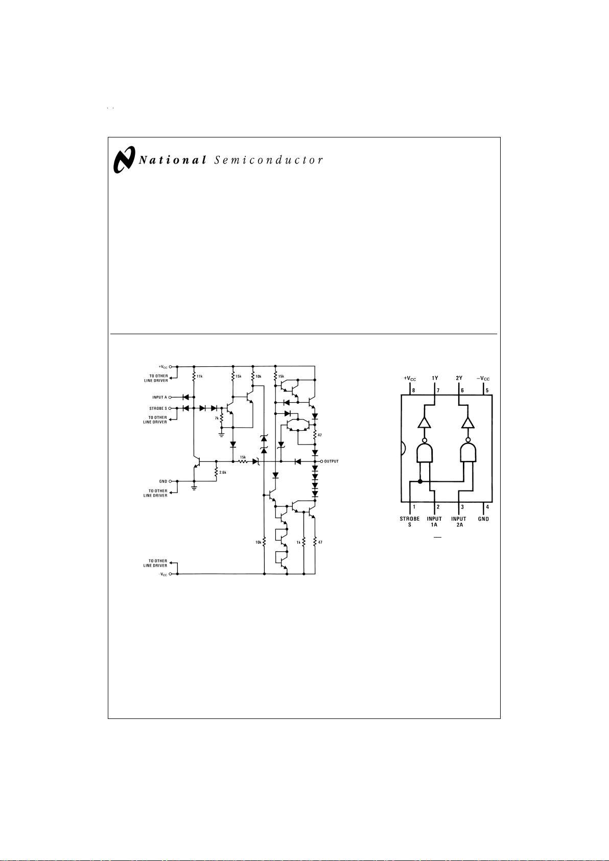
Schematic and Connection Diagrams
DS005794-1
Component values shown are nominal.
1/2 of circuit shown
Dual-In-Line Package
DS005794-2
Positive Logic C=AS
Top View
Order Number DS75150M
See NS Package Number M08A
May 1998
DS75150 Dual Line Driver
© 1998 National Semiconductor Corporation DS005794 www.national.com
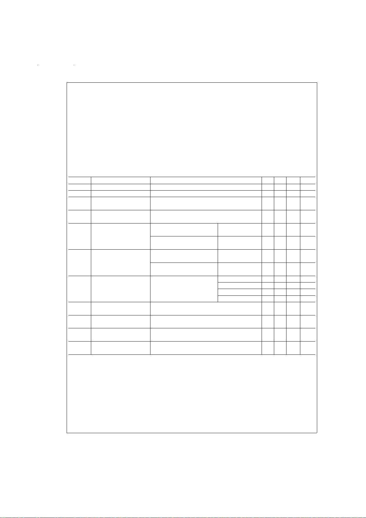
Absolute Maximum Ratings (Note 2)
If Military/Aerospace specified devices are required,
please contact the National Semiconductor Sales Office/
Distributors for availability and specifications.
Supply Voltage +V
CC
15V
Supply Voltage −V
CC
15V
Input Voltage 15V
Applied Output Voltage +25V
Storage Temperature Range −65˚C to +150˚C
Maximum Power Dissipation (Note 1) at 25˚C
SO Package 655 mW
Lead Temperature (Soldering, 4
sec.) 260˚C
Operating Conditions
Min Max Units
Supply Voltage (+V
CC
) 10.8 13.2 V
Supply Voltage (−V
CC
) −10.8 −13.2 V
Input Voltage (V
I
) 0 +5.5 V
Output Voltage (V
O
)
±
15 V
Operating Ambient Temperature
Range (T
A
) 0 +70 ˚C
Note 1: Derate SO package 8.01 mW/˚C above 25˚C.
DC Electrical Characteristics (Notes 3, 4, 5, 6)
Symbol Parameter Conditions Min Typ Max Units
V
IH
High-Level Input Voltage
(Figure 1 )
2V
V
IL
Low-Level Input Voltage (
Figure 2
) 0.8 V
V
OH
High-Level Output Voltage +V
CC
=
10.8V,−V
CC
=
−13.2V, V
IL
=
0.8V, 5 8 V
R
L
=
3kΩto7kΩ(
Figure 2
)
V
OL
Low-Level Output Voltage +V
CC
=
10.8V,−V
CC
=
−10.8V, V
IH
=
2V, −8 −5 V
R
L
=
3kΩto7kΩ(
Figure 1
)
I
IH
High-Level Input Current +V
CC
=
13.2V,−V
CC
=
−13.2V, Data Input 1 10 µA
V
I
=
2.4V, (
Figure 3
)
+V
CC
=
13.2V, −V
CC
=
−13.2V, Strobe Input 2 20 µA
V
I
=
2.4V, (
Figure 3
)
I
IL
Low-Level Input Current +V
CC
=
13.2V,−V
CC
=
−13.2V, Data Input −1 −1.6 mA
V
I
=
0.4V, (
Figure 3
)
+V
CC
=
13.2V, −V
CC
=
−13.2V, Strobe Input −2 −3.2 mA
V
I
=
0.4V, (
Figure 3
)
I
OS
Short-Circuit Output Current +V
CC
=
13.2V,−V
CC
=
−13.2V, V
O
=
25V 2 5 mA
(
Figure 4
), (Note 5) V
O
=
−25V −3 −6 mA
V
O
=
0V, V
I
=
3V 15 30 mA
V
O
=
0V, V
I
=
0V −15 −30 mA
+I
CCH
Supply Current From +VCC,+V
CC
=
13.2V, −V
CC
=
−13.2V, V
I
=
0V, 10 22 mA
High-Level Output R
L
=
3kΩ,T
A
=
25˚C, (
Figure 5
)
−I
CCH
Supply Current From −VCC,+V
CC
=
13.2V, −V
CC
=
−13.2V, V
I
=
0V, −1 −10 mA
High-Level Output R
L
=
3kΩ,T
A
=
25˚C, (
Figure 5
)
+I
CCL
Supply Current From +VCC,+V
CC
=
13.2V, −V
CC
=
−13.2V, V
I
=
3V, 8 17 mA
Low-Level Output R
L
=
3kΩ,T
A
=
25˚C, (
Figure 5
)
−I
CCL
Supply Current From −VCC,+V
CC
=
13.2V, −V
CC
=
−13.2V, V
I
=
3V, −9 −20 mA
Low-Level Output R
L
=
3kΩ,T
A
=
25˚C, (
Figure 5
)
Note 2: “Absolute Maximum Ratings”arethose values beyond which the safety of the device cannot be guaranteed. Except for “Operating TemperatureRange” they
are not meant to imply that the devices should be operated at these limits. The table of “Electrical Characteristics” provides conditions for actual device operation.
Note 3: Unless otherwise specified min/max limits apply across the 0˚C to +70˚C range for the DS75150. All typical values are T
A
=
25˚C and +V
CC
=
12V, −V
CC
=
−12V.
Note 4: All current into device pins shown as positive, out of device pins as negative, all voltages referenced to ground unless otherwise noted. All values shown
as max or min on absolute value basis.
Note 5: Only one output at a time should be shorted.
Note 6: The algebraic convention where the most-positive (least-negative) limit is designated as maximum is used in this data sheet for logic levels only,e.g., when
−5V is the maximum, the typical value is more-negative voltage.
www.national.com 2
 Loading...