

NSC DS75107N, DS75107MX, DS75107M Datasheet
DS75107
Dual Line Receiver
General Description
The product described herein is a TTL compatible dual high
speed circuitintended for sensing in a broad range of system
applications. While the primary usage will be for line receivers of MOS sensing, the product may effectively be used as
a voltage comparator, level translator, window detector,
transducer preamplifier, and in other sensing applications.
As a digital line receiver the product is applicable with the
SN55109/SN75109 and µA75110/DS75110 companion drivers, or may be used in other balanced or unbalanced
party-line data transmission systems.
Input protection diodes are incorporated in series with the
collectors of the differential input stage. These diodes are
useful in certain applications that have multiple V
CC
+ sup-
plies or V
CC
+ supplies that are turned off.
Features
n Diode protected input stage for power “OFF” condition
n 17 ns typ high speed
n TTL compatible
n
±
10 mV or±25 mV input sensitivity
n
±
3V input common-mode range
n High input impedance with normal V
CC
,orV
CC
=
0V
n Strobes for channel selection
n Dual circuits
n Sensitivity gntd. over full common-mode range
n Logic input clamp diodes—meets both “A” and “B”
version specifications
n
±
5V standard supply voltages
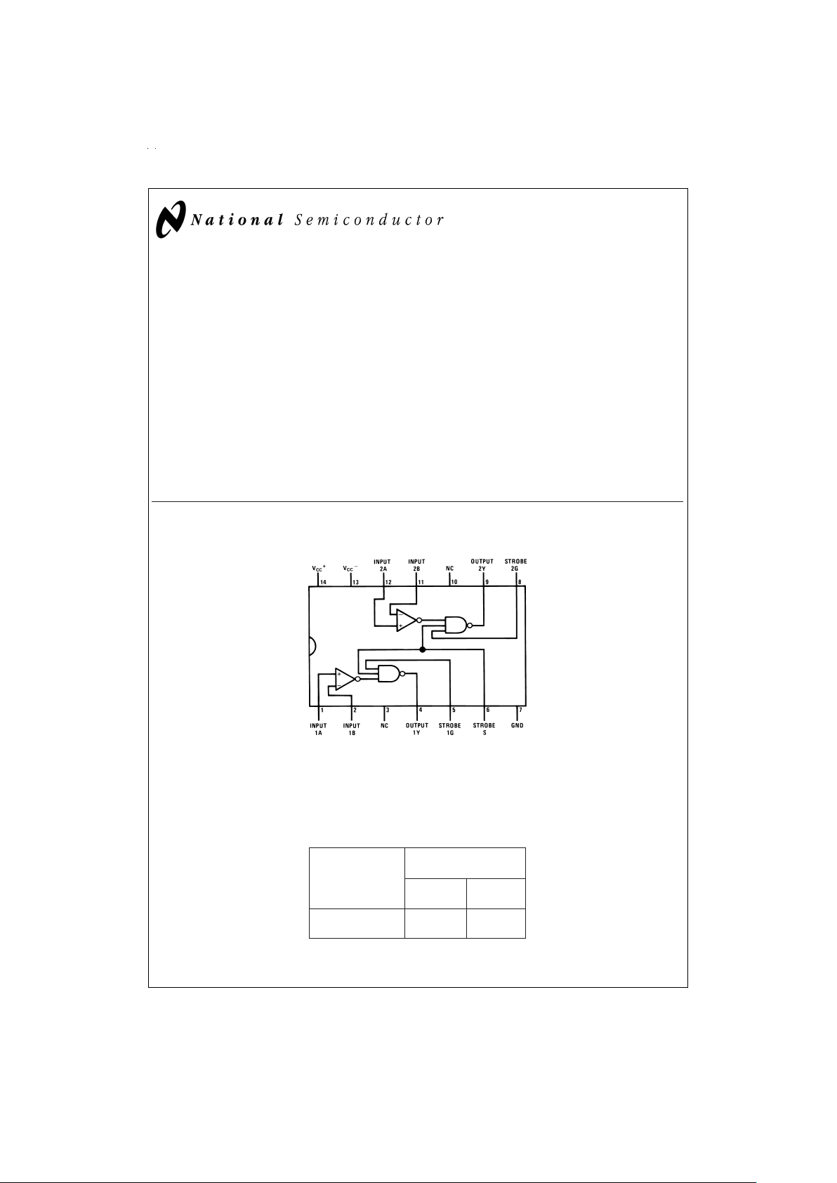
Connection Diagram
Selection Guide
Temperature
→
0˚C ≤ TA≤ +70˚C
Package
→
Cavity or Molded Dip
Input Sensitivity
→
±
25 mV
±
10 mV
Output Logic
↓
TTL Active Pull-Up DS75107
TTL Open Collector
Dual-In-Line Package
DS009446-1
Top View
Order Number DS75107M, DS75107N
See NS Package Number M14A or N14A
For Complete Military 883 Specifications, see RETS Datasheet.
Order Number DS55107AJ/883
See NS Package Number J14A
May 1999
DS75107 Dual Line Receiver
© 1999 National Semiconductor Corporation DS009446 www.national.com
Absolute Maximum Ratings (Note 1)
If Military/Aerospace specified devices are required,
please contact the NationalSemiconductor Sales Office/
Distributors for availability and specifications.
Supply Voltage, V
CC
+7V
Supply Voltage, V
CC
− −7V
Differential Input Voltage
±
6V
Common Mode Input Voltage
±
5V
Strobe Input Voltage 5.5V
Storage Temperature Range −65˚C to +150˚C
Maximum Power Dissipation (Note 1) at 25˚C
Cavity Package 1308 mW
Molded Package 1207 mW
Lead Temperature (Soldering, 4 sec) 260˚C
Note: Derate cavity package 8.7mW/˚C above 25˚C; derate moldedpackage
9.7 mW/˚C above 25˚C.
Operating Conditions
DS75107
Min Nom Max
Supply Voltage V
CC
+ 4.75V 5V 5.25V
Supply Voltage V
CC
− −4.75V −5V −5.25V
Operating Temperature Range 0˚C to +70˚C
DS75107
Electrical Characteristics
T
MIN
≤ TA≤ T
MAX
(Notes 2, 3)
Symbol Parameter Conditions Min Typ Max Units
I
IH
High Level Input Current V
CC+
=
Max, V
CC−
=
Max, 30 75
µA
into A1, B1, A2 or B2 V
ID
=
0.5V, V
IC
=
−3V to 3V
I
IL
Low Level Input Current V
CC+
=
Max, V
CC−
=
Max, −10
µA
into A1, B1, A2 or B2 V
ID
=
−2V, V
IC
=
−3V to 3V
I
IH
High Level Input Current V
CC+
=
Max, V
IH(S)
=
2.4V 40 µA
into G1 or G2 V
CC−
=
Max V
IH(S)
Max V
CC+
1mA
I
IL
Low Level Input Current V
CC+
=
Max, V
CC−
=
Max, −1.6
mA
into G1 or G2 V
IL(S)
=
0.4V
I
IH
High Level Input Current into S V
CC+
=
Max, V
IH(S)
=
2.4V 80 µA
V
CC−
=
Max V
IH(S)
=
Max V
CC+
2mA
I
IL
Low Level Input Current into S V
CC+
=
Max, V
CC−
=
Max, −3.2
mA
V
IL(S)
=
0.4V
V
OH
High Level Output Voltage V
CC+
=
Min, V
CC−
=
Min,
I
LOAD
=
−400 µA, V
ID
=
25 mV, 2.4 V
V
IC
=
−3V to 3V, (Note 3)
V
OL
Low Level Output Voltage V
CC+
=
Min, V
CC−
=
Min,
I
SINK
=
16 mA, V
ID
=
−25 mV, 0.4 V
V
IC
=
−3V to 3V
I
OH
High Level Output Current V
CC+
=
Min, V
CC−
=
Min 250
µA
V
OH
=
Max V
CC+
I
OS
Short Circuit Output Current V
CC+
=
Max, V
CC−
=
Max, −18 −70
mA
(Notes 3, 5)
I
CCH+
High Logic Level Supply V
CC+
=
Max, V
CC−
=
Max, 18 30
mA
Current from V
CC
V
ID
=
25 mV, T
A
=
25˚C
I
CCH−
High Logic Level Supply V
CC+
=
Max, V
CC−
=
Max, −8.4 −15
mA
Current from V
CC
V
ID
=
25 mV, T
A
=
25˚C
V
I
Input Clamp Voltage on G or S V
CC+
=
Min, V
CC−
=
Min, −1 −1.5
V
I
IN
=
−12 mA, T
A
=
25˚C
www.national.com 2
Switching Characteristics
V
CC+
=
5V, V
CC−
=
−5V, T
A
=
25˚C
Symbol Parameter Conditions Min Typ Max Units
t
PLH(D)
Propagation Delay Time, Low to
High Level, from Differential Inputs
A and B to Output
R
L
=
390Ω,C
L
=
50 pF,
(Note 4)
17 25 ns
19 25 ns
t
PHL(D)
Propagation Delay Time, High to
Low Level, from Differential Inputs
A and B to Output
R
L
=
390Ω,C
L
=
50 pF,
(Note 4)
17 25 ns
19 25 ns
t
PLH(S)
Propagation Delay Time, Low to
High Level, from Strobe Input G or
S to Output
R
L
=
390Ω,C
L
=
50 pF 10 15 ns
13 20 ns
t
PHL(S)
Propagation Delay Time, High to
Low Level, from Strobe Input G or
S to Output
R
L
=
390Ω,C
L
=
50 pF 8 15 ns
13 20 ns
Switching Characteristics
V
CC+
=
5V, V
CC−
=
−5V, T
A
=
25˚C
Symbol Parameter Conditions Min Typ Max Units
t
PLH(D)
Propagation Delay Time, Low-to- R
L
=
470Ω,C
L
=
15 pF, (Note 6)
High Level, from Differential 35 ns
Inputs A and B to Output
t
PHL(D)
Propagation Delay Time, High-to- R
L
=
470Ω,C
L
=
15 pF, (Note 6)
Low Level, from Differential 20 ns
Inputs A and B to Output
t
PLH(S)
Propagation Delay Time, Low-to- R
L
=
470Ω,C
L
=
15 pF
High Level, from Strobe Input G 17 ns
or S to Output
t
PHL(S)
Propagation Delay Time, High-to- R
L
=
470Ω,C
L
=
15 pF
Low Level, from Strobe Input G 17 ns
or S to Output
Note 1: “Absolute MaximumRatings” are those valuesbeyond which the safety of the device cannot beguaranteed. Except for “OperatingTemperature Range” they
are not meant to imply that the devices should be operated at these limits. The table of “Electrical Characteristics” provides conditions for actual device operation.
Note 2: Unless otherwise specified min/max limits apply across the 0˚C to +70˚C range for the DS75107. All typical values are for T
A
=
25˚C and V
CC
=
5V.
Note 3: All currents into device pins shown as positive, out of device pins as negative, all voltages referenced to ground unless otherwise noted. All values shown
as max or min on absolute value basis.
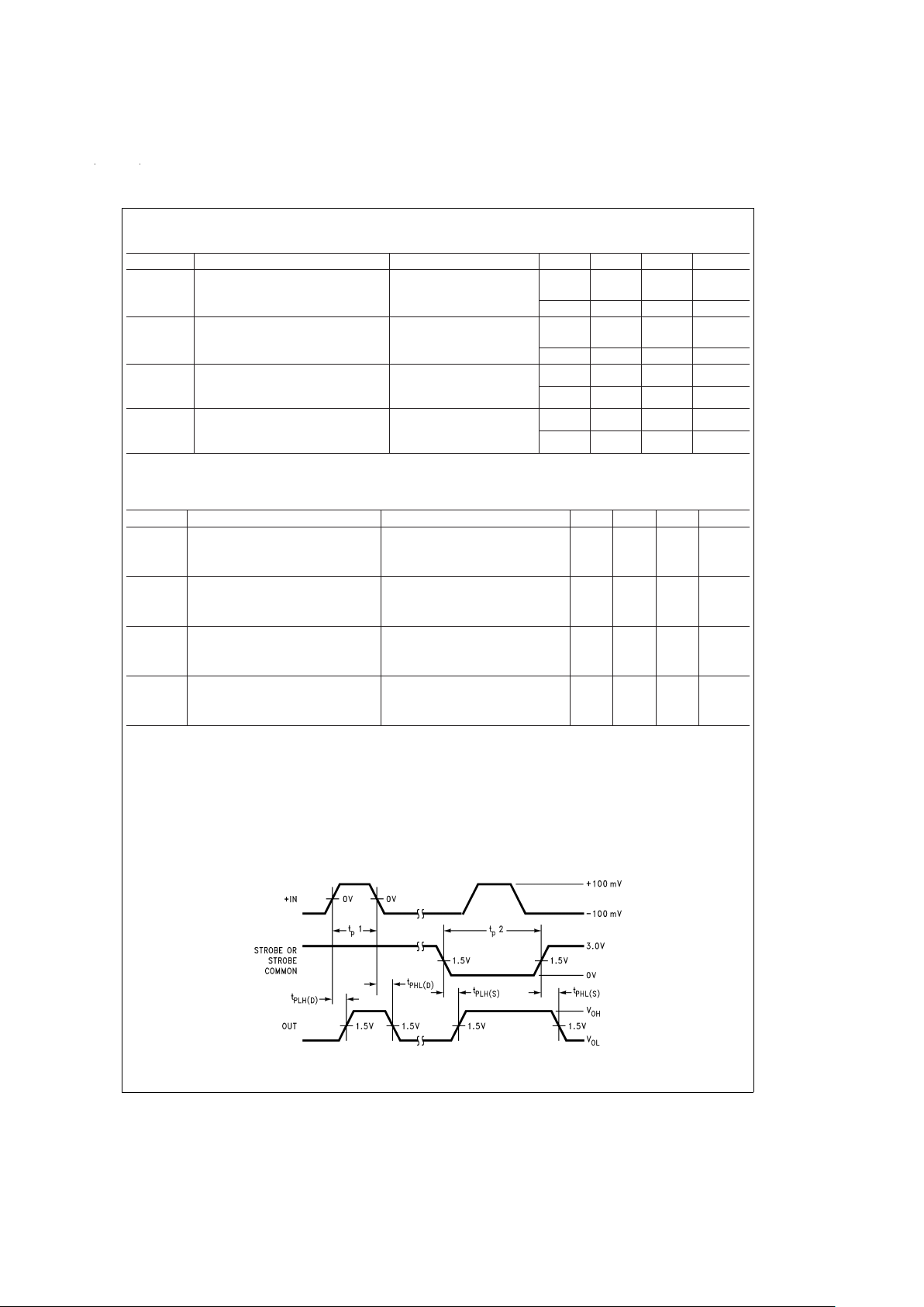
Note 4: Differential input is +100 mV to −100 mV pulse. Delays read from 0 mV on input to 1.5V on output.
Note 5: Only one output at a time should be shorted.
Note 6: Differential input is +10 mV to −30 mV pulse. Delays read from 0 mV on input to 1.5V on output.
Voltage Waveforms
DS009446-12
www.national.com3
 Loading...