

February 7, 2008
DS50EV401
2.5 Gbps / 5.0 Gbps / 8.0 Gbps Quad PCI Express Cable and
Backplane Equalizer
General Description
The DS50EV401 is a low power, programmable equalizer
specifically designed for PCI Express applications. The device provides 2 equalization settings to reduce inter-symbol
interference (ISI) induced by a variety of interconnect media.
One setting is optimized for PCIe Gen1 and Gen2 applications; the other is optimized for future Gen3 data rates. In all
modes, the equalizer can operate, error free, with an input eye
that is completely closed by interconnect ISI. A single pin,
MODE, allows the user to change between these two modes.
The DS50EV401 enables PCI Express compatible link extension by supporting transmit electrical idle, and Beacon
signal pass through on a per lane basis. Current-mode logic
(CML) is used on both input and output terminals, which provide constant 50 ohm single-ended impedance to AC ground.
Differential signaling is implemented through out the entire
signal path to minimize supply induced jitter. The DS50EV401
is available in a 7mm x 7mm 48-pin leadless LLP package,
and is powered from a single power supply of either 3.3 or
2.5V.
Features
■
PCI Express compatible link extension
■
Automatic power management on an individual lane basis
■
Data rate optimized equalization
■
Operates over 7 meter of 24 AWG PCI Express Cables up
to 8 Gbps
■
0.18 UI of residual deterministic jitter at 8 Gbps with 30” of
FR4
■
0.18 UI of residual deterministic jitter at 5 Gbps with 40” of
FR4
■
0.16 UI of residual deterministic jitter at 2.5 Gbps with 40”
of FR4
■
8 kV HBM ESD
■
-40 to 85°C operating temperature range
■
7 mm x 7 mm 48-pin leadless LLP package
■
Single power supply of either 3.3V or 2.5V
■
Low power (typically 95 mW per channel at 2.5V VCC)
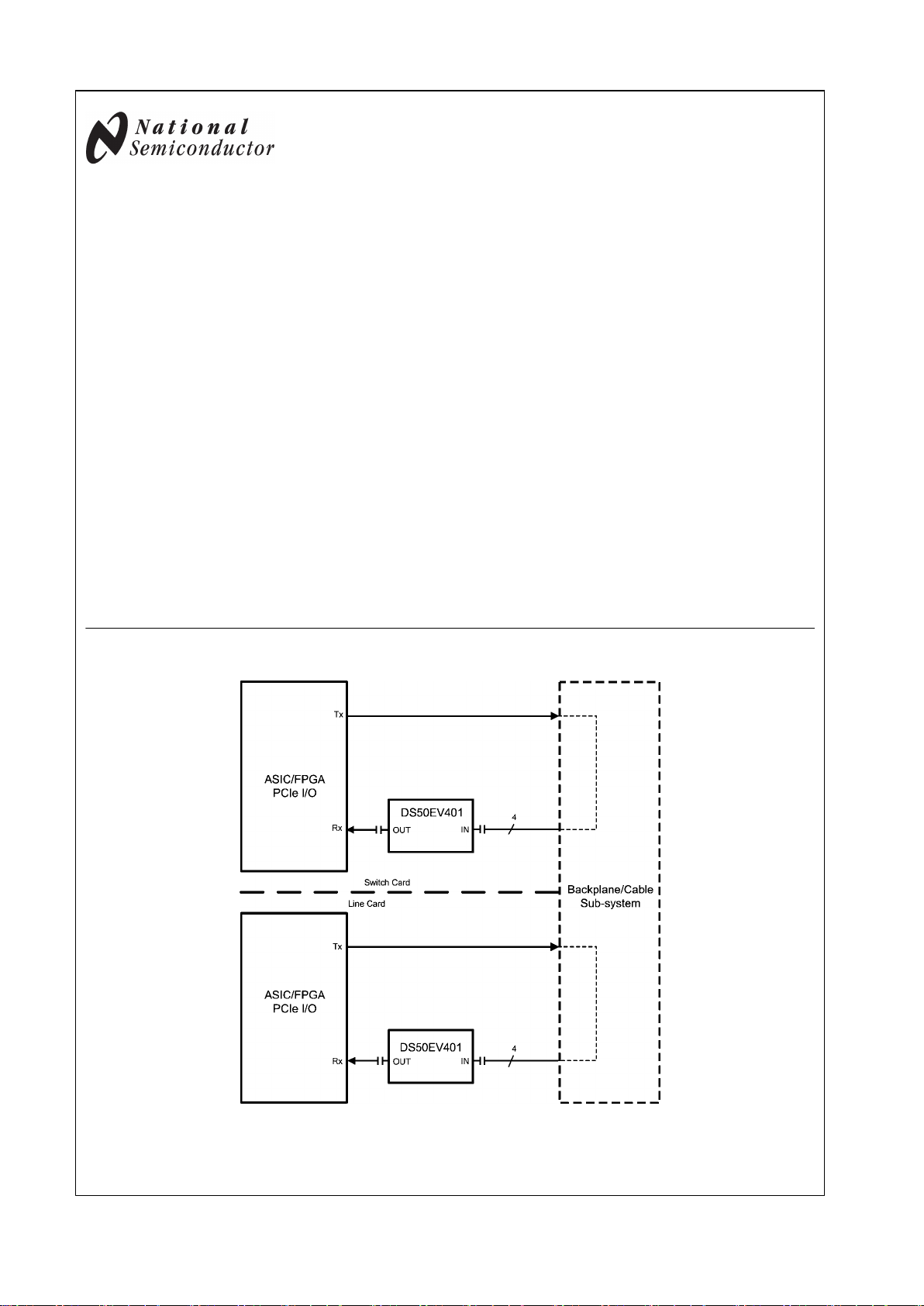
Simplified Application Diagram
30050524
© 2008 National Semiconductor Corporation 300505 www.national.com
DS50EV401 2.5 Gbps / 5.0 Gbps / 8.0 Gbps Quad PCI Express Cable and Backplane Equalizer
Pin Descriptions
Pin Name Pin Number I/O, Type Description
HIGH SPEED DIFFERENTIAL I/O
IN_0+
IN_0-
1
2
I, CML
Inverting and non-inverting CML differential inputs to the equalizer. An on-chip 50Ω
terminating resistor connects IN_0+ to VDD and IN_0- to VDD.
IN_1+
IN_1-
4
5
I, CML
Inverting and non-inverting CML differential inputs to the equalizer. An on-chip 50Ω
terminating resistor connects IN_1+ to VDD and IN_1- to VDD.
IN_2+
IN_2-
8
9
I, CML
Inverting and non-inverting CML differential inputs to the equalizer. An on-chip 50Ω
terminating resistor connects IN_2+ to VDD and IN_2- to VDD.
IN_3+
IN_3-
11
12
I, CML
Inverting and non-inverting CML differential inputs to the equalizer. An on-chip 50Ω
terminating resistor connects IN_3+ to VDD and IN_3- to VDD.
OUT_0+
OUT_0-
36
35
O, CML
Inverting and non-inverting CML differential outputs from the equalizer. An on-chip 50Ω
terminating resistor connects OUT_0+ to VDD and OUT_0- to VDD.
OUT_1+
OUT_1-
33
32
O, CML
An on-chip 50Ω terminating resistor connects OUT_1+ to VDD and OUT_1- to VDD.
OUT_2+
OUT_2-
29
28
O, CML
Inverting and non-inverting CML differential outputs from the equalizer. An on-chip 50Ω
terminating resistor connects OUT_2+ to VDD and OUT_2- to VDD.
OUT_3+
OUT_3-
26
25
O, CML
Inverting and non-inverting CML differential outputs from the equalizer. An on-chip 50Ω
terminating resistor connects OUT_3+ to VDD and OUT_3- to VDD.
EQUALIZATION CONTROL
MODE 14 I, CMOS MODE selects the equalizer frequency for EQ channels. MODE is internally pulled low.
DEVICE CONTROL
EN0 44 I, CMOS Enable Ch0 output driver input. When held High, normal operation is selected. When held
Low, Ch0 output drive is off and standby mode is selected. EN0 is internally pulled High.
EN1 42 I, CMOS Enable Ch1 output driver input. When held High, normal operation is selected. When held
Low, Ch1 output drive is off and standby mode is selected. EN1 is internally pulled High.
EN2 40 I, CMOS Enable Ch2 output driver input. When held High, normal operation is selected. When held
Low, Ch2 output drive is off and standby mode is selected. EN2 is internally pulled High.
EN3 38 I, CMOS Enable Ch3 output driver input. When held High, normal operation is selected. When held
Low, CH3 output drive is off and standby mode is selected. EN3 is internally pulled High.
SD0 45 O, CMOS Equalizer Ch0 Signal Detect Output. Produces a High when signal is detected.
SD1 43 O, CMOS Equalizer Ch1 Signal Detect Output. Produces a High when signal is detected.
SD2 41 O, CMOS Equalizer Ch2 Signal Detect Output. Produces a High when signal is detected.
SD3 39 O, CMOS Equalizer Ch3 Signal Detect Output. Produces a High when signal is detected.
POWER
V
DD
3, 6, 7,
10, 13,
15, 46
Power VDD = 2.5V ± 5% or 3.3V ± 10%. VDD pins should be tied to VDD plane through low inductance
path. A 0.01μF bypass capacitor should be connected between each VDD pin to GND planes.
GND 22, 24,
27, 30,
31, 34
Power Ground reference. GND should be tied to a solid ground plane through a low impedance
path.
Exposed
Pad
PAD Power Ground reference. The exposed pad at the center of the package must be connected to
ground plane of the board.
OTHER
Reserv 16, 17, 18,
19, 20, 21,
23, 37, 47,
48
Reserved. Do not connect.
Note: I = Input O = Output
www.national.com 2
DS50EV401
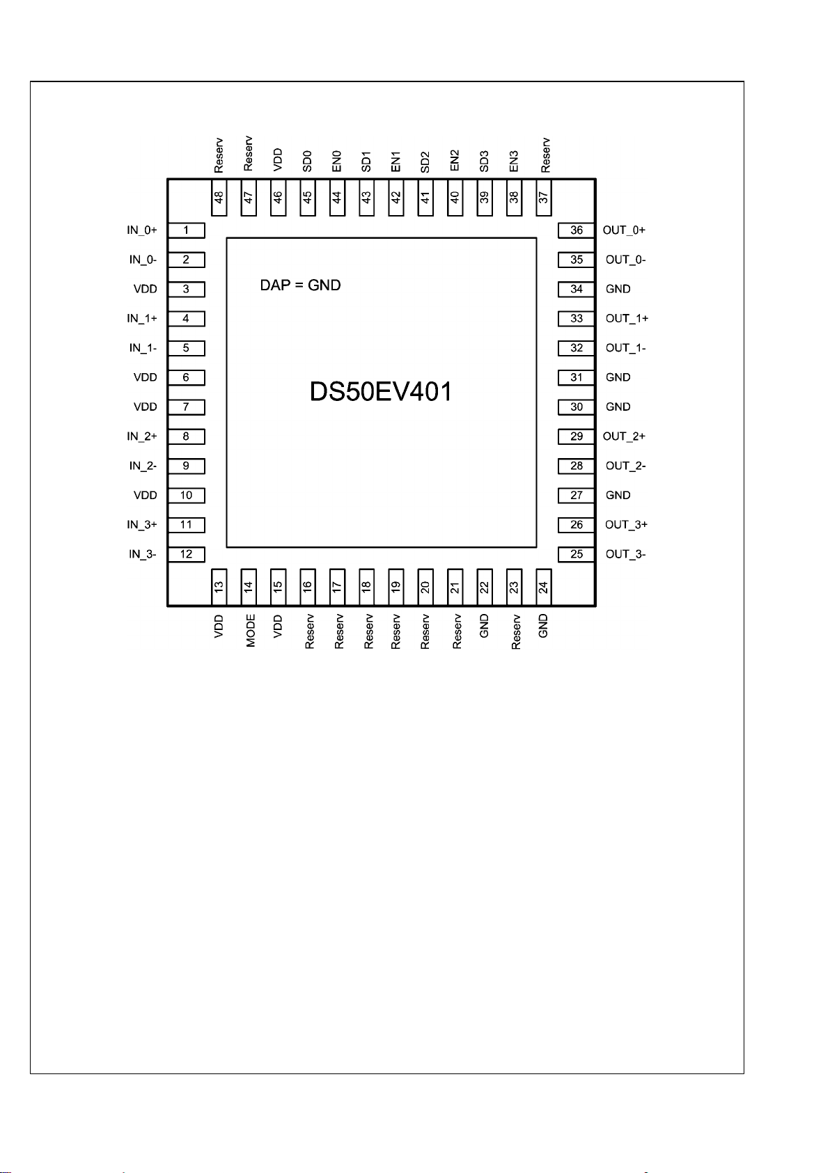
Connection Diagram
30050526
3 www.national.com
DS50EV401
Absolute Maximum Ratings (Note 1)
If Military/Aerospace specified devices are required,
please contact the National Semiconductor Sales Office/
Distributors for availability and specifications.
Supply Voltage (VDD)
−0.5V to +4.0V
CMOS Input Voltage −0.5V + 4.0V
CMOS Output Voltage −0.5V to 4.0V
CML Input/Output Voltage −0.5V to 4.0V
Junction Temperature +150°C
Storage Temperature −65°C to +150°C
Lead Temperature (Soldering, 4
Seconds)
+260°C
ESD Rating
HBM, 1.5 kΩ, 100 pF
>8 kV
Thermal Resistance
θJA, No Airflow
30°C/W
Recommended Operating
Conditions
Min Typ Max Units
Supply Voltage
V
DD2.5
to GND 2.375 2.5 2.625 V
V
DD3.3
to GND 3.0 3.3 3.6 V
Ambient Temperature −40 25 +85 °C
Electrical Characteristics
Over recommended operating supply and temperature ranges with default register settings unless other specified. (Note 2, 3)
Symbol Parameter Conditions Min Typ Max Units
POWER
P Power Supply Consumption Device Enabled, V
DD3.3
510
700
mW
Device Disabled, V
DD3.3
100 mW
P Power Supply Consumption Device Enabled, V
DD2.5
380
490
mW
Device Disabled, V
DD2.5
30
mW
N Supply Noise Tolerance
(Note 4)
Upto 50 MHz
100
mV
P-P
LVTTL DC SPECIFICATIONS
V
IH
High Level Input Voltage V
DD3.3
2.0
V
DD
V
V
DD2.5
1.6
V
DD
V
V
IL
Low Level Input Voltage -0.3
0.8
V
V
OH
High Level Output Voltage IOH = -3mA, V
DD3.3
2.4
V
IOH = -3mA, V
DD2.5
2.0
V
V
OL
Low Level Output Voltage IOL = 3mA
0.4
V
I
IN
Input Current VIN = V
DD
+15
μA
VIN = GND -15
μA
I
IN-P
Input Leakage Current with
Internal Pull-Down/Up Resistors
VIN = VDD,
with internal pull-down resistors
+140
μA
VIN = VDD,
with internal pull-up resistors
-40
μA
CML RECEIVER INPUTS (IN_n+, IN_n-)
V
IN
Input Voltage Swing AC-Coupled or DC-Coupled
Required Differential Amplitude
measured at point A
(Figure 1)
400 1600
mV
P-P
V
IN-S
Input Voltage Sensitivity AC-Coupled or DC-Coupled
Required Differential Envelope
measured at point B
(Figure 1, 10) (Note 5)
170
mV
P-P
R
LI
Differential Input Return Loss 100 MHz – 4.0 GHz, with fixture’s
effect de-embedded
10 dB
R
IN
Input Resistance Single ended to VDD
40 50 60
Ω
www.national.com 4
DS50EV401
Symbol Parameter Conditions Min Typ Max Units
CML OUTPUTS (OUT_n+, OUT_n-)
V
O
Output Voltage Swing Differential measurement with
OUT_n+ and OUT_n- terminated
by 50Ω to GND AC-Coupled
(Figure 2)
800 1200
mV
P-P
V
OCM
Output Common-Mode Voltage Single-ended measurement DC-
Coupled with 50Ω termination
(Note 6)
VDD – 0.25
V
tR, t
F
Transition Time 20% to 80% of differential output
voltage, measured within 1” from
output pins
(Figure 2) (Note 6)
40 ps
R
O
Output Resistance Single-ended to V
DD
40 50 60
Ω
R
LO
Differential Output Return Loss 100 MHz – 4.0 GHz, with fixture’s
effect de-embedded. IN_n+ =
static high
10 dB
t
PLHD
Differential Low to High
Propagation Delay
Propagation delay measurement
at 50% VO between input to output,
100 Mbps
(Figure 3) (Note 8)
240 ps
t
PHLD
Differential High to Low
Propagation Delay
240 ps
t
ID
Idle to Valid Differential Data VIN = 800 mVp-p, 5 Gbps, EIEOS,
40” of 6 mil microstrip FR4
(Figure 4) (Note 6)
8 ns
t
DI
Valid Differential data to idle VIN = 800 mVp-p, 5 Gbps, EIOS,
40” of 6 mil microstrip FR4
(Figure 4) (Note 6)
8 ns
t
CCSK
Inter Pair Channel to Channel
Skew
Difference in 50% crossing
between channels
7 ps
EQUALIZATION
DJ1 Residual Deterministic Jitter at 8
Gbps
30” of 6 mil microstrip FR4,
MODE=0, PRBS-7 (27-1) pattern
(Note 6, 7)
0.18
UI
P-P
DJ2 Residual Deterministic Jitter at 5
Gbps
40” of 6 mil microstrip FR4,
MODE=1, PRBS-7 (27-1) pattern
(Note 6, 7)
0.18 0.21
UI
P-P
DJ3 Residual Deterministic Jitter at 2.5
Gbps
40” of 6 mil microstrip FR4,
MODE=1, PRBS-7 (27-1) pattern
(Note 6, 7)
0.16 0.18
UI
P-P
RJ Random Jitter (Note 8, 9) 0.5 psrms
Note 1: “Absolute Maximum Ratings” indicate limits beyond which damage to the device may occur, including inoperability and degradation of device reliability
and/or performance. Functional operation of the device and/or non-degradation at the Absolute Maximum Ratings or other conditions beyond those indicated in
the Recommended Operating Conditions is not implied. The Recommended Operating Conditions indicate conditions at which the device is functional and the
device should not be operated beyond such conditions. Absolute Maximum Numbers are guaranteed for a junction temperature range of -40°C to +125°C. Models
are validated to Maximum Operating Voltages only.
Note 2: Typical values represent most likely parametric norms at VDD = 3.3V or 2.5V, TA = 25°C., and at the Recommended Operation Conditions at the time of
product characterization and are not guaranteed.
Note 3: The Electrical Characteristics tables list guaranteed specifications under the listed Recommended Operating Conditions except as otherwise modified
or specified by the Electrical Characteristics Conditions and/or Notes. Typical specifications are estimations only and are not guaranteed.
Note 4: Allowed supply noise (mV
P-P
sine wave) under typical conditions.
Note 5: V
IN-S
is a measurement of the input differential envelope (Figure 10). The device does not require an open eye.
Note 6: Specification is guaranteed by characterization at optimal MODE setting and is not tested in production.
Note 7: Deterministic jitter is measured at the differential outputs (point C of Figure 1), minus the deterministic jitter before the test channel (point A of Figure 1).
Random jitter is removed through the use of averaging or similar means.
Note 8: Measured with clock-like {11111 00000} pattern.
Note 9: Random jitter contributed by the equalizer is defined as sqrt (J
OUT
2
– J
IN
2
). J
OUT
is the random jitter at equalizer outputs in ps-rms, see point C of Figure
1; JIN is the random jitter at the input of the equalizer in ps-rms, see point B of Figure 1.
5 www.national.com
DS50EV401

Timing Diagrams
30050527
FIGURE 1. Test Setup Diagram
30050502
FIGURE 2. CML Output Transition Times
30050503
FIGURE 3. Propagation Delay Timing Diagram
www.national.com 6
DS50EV401

30050504
FIGURE 4. Idle Timing Diagram
7 www.national.com
DS50EV401

DS50EV401 Applications
Information
The DS50EV401 is a programmable quad equalizer optimized for PCI Express applications. It is designed to operate
over copper backplanes and cables at transmission rates of
2.5 Gbps up to 8 Gbps. The device consists of an input receive equalizer followed by a limiting amplifier. The equalizer
is designed to open an input eye that is completely closed due
to inter-symbol interference (ISI) induced by the channel interconnect. The equalization is set to keep residual deterministic jitter below 0.2 unit intervals (UI) regardless of data rate.
This equalization scheme allows 1 equalization setting to satisfy both Gen1 and Gen2 links, eliminating the need for interaction between the equalizer and PCI Express endpoint
during link negotiation. The DS50EV401 is intended as a unidirectional receiver that should be placed in close physical
proximity to the end point. Therefore the transmitter does not
include de-emphasis as TX equalization would not be needed
over the short distance between the equalizer and the end
point.
In order to enable PCI compliant link extension the
DS50EV401 will put the transmitter into electrical idle mode
when no active data is sensed on its inputs. Idle is controlled
on a per lane basis, and is solely dependent on activity of a
particular channel’s input activity. 50 ohm termination is maintained on both the RX and TX terminals in electrical idle mode.
The DS50EV401 internal signal path is designed to be broad
band, allowing the Beacon Wakeup signal to pass through to
the endpoint device.
30050505
FIGURE 5. Simplified Block Diagram
DATA CHANNELS
The DS50EV401 consists of four data channels. Each channel provides input termination, receiver equalization, signal
limiting, offset cancellation, and a CML output driver, as
shown in Figure 5. The data channels support two levels of
equalization, controlled by the pin MODE. The equalization
levels are set simultaneously on all 4 channels, as described
in Table 1.
When an idle condition is sensed on a channel’s input, the
transmit driver is automatically placed into electrical idle
mode, as shown in Figure 6. The common mode voltage is
set, and the differential output is forced to zero. To save power, the output driver current is powered off when the device is
in electrical idle mode. All other circuits maintain their bias
currents allowing a fast recovery from idle to the active state.
Electric idle is performed on a per channel basis, and several
channels can be in idle while others are actively passing data.
TABLE 1. MODE Control Table
6 mil microstrip FR4
trace length (in)
24 AWG Twin-AX cable
length (m)
Frequency Channel Loss MODE
0–30 0–7 8 Gbps 16 dB 0
0–40 0–10 5 Gbps
2.5 Gbps
14 dB
20 dB
1
30050506
FIGURE 6. Automatic Power Management
www.national.com 8
DS50EV401

BEACON WAKEUP
The DS50EV401 signal path is designed to be broadband,
allowing a low frequency signal, such as the Beacon Wakeup
used by the PCI Express protocol, to pass through the device.
The AC coupling capacitors used to connect the DS50EV401
to the rest of the system limit the fidelity of the Beacon signal.
Therefore, a minimum capacitance of 75nF, as shown in figure 7, is required for proper operation.
30050507
FIGURE 7. Example of Passing Beacon Signal
GENERAL RECOMMENDATIONS
The DS50EV401 is a high performance device capable of
delivering excellent performance. In order to extract full performance from the device in a particular application, good
high-speed design practices must be followed. National
Semiconductor’s LVDS Owner's Manual, 4th edition provides
detailed information about managing signal integrity and power delivery to get the most from your design.
PCB LAYOUT CONSIDERATIONS FOR DIFFERENTIAL
PAIRS
The CML inputs and outputs must have a controlled differential impedance of 100Ω. It is preferable to route CML lines
exclusively on one layer of the board, particularly for the input
traces. The use of vias should be avoided if possible. If vias
must be used, they should be used sparingly and must be
placed symmetrically for each side of a given differential pair.
Route the CML signals away from other signals and noise
sources on the printed circuit board. See AN-1187 for additional information on LLP packages..
POWER SUPPLY BYPASSING
Two approaches are recommended to ensure that the
DS50EV401 is provided with an adequate power supply.
First, the supply (VDD) and ground (GND) pins should be
connected to power planes routed on adjacent layers of the
printed circuit board. The layer thickness of the dielectric
should be minimized so that the VDD and GND planes create
a low inductance supply with distributed capacitance. Second, careful attention to supply bypassing through the proper
use of bypass capacitors is required. A 0.01μF bypass capacitor should be connected to each VDD pin such that the
capacitor is placed as close as possible to the DS50EV401.
Smaller body size capacitors can help facilitate proper component placement. Additionally, three capacitors with capacitance in the range of 2.2 μF to 10 μF should be incorporated
in the power supply bypassing design as well. These capacitors can be either tantalum or an ultra-low ESR ceramic and
should be placed as close as possible to the DS50EV401.
9 www.national.com
DS50EV401

Typical Performance Eye Diagrams and Curves
30050508
Figure 8. Unequalized Signal (40 in FR4, 2.5 Gbps, PRBS7)
30050509
Figure 9. Equalized Signal (40 in FR4, 2.5 Gbps, PRBS7,
MODE=1)
30050510
Figure 10. Unequalized Signal (40 in FR4, 5 Gbps, PRBS7)
30050511
Figure 11. Equalized Signal (40 in FR4, 5 Gbps, PRBS7,
MODE=1)
30050512
Figure 12. Unequalized Signal (30 in FR4, 8 Gbps, PRBS7)
30050513
Figure 13. Equalized Signal (30 in FR4, 8 Gbps, PRBS7,
MODE=0)
www.national.com 10
DS50EV401

30050514
Figure 14. Unequalized Signal (10 m 24 AWG Twin-AX
Cable, 2.5 Gbps, PRBS7)
30050515
Figure 15. Equalized Signal (10 m 24 AWG Twin-AX
Cable, 2.5 Gbps, PRBS7, MODE=1)
30050516
Figure 16. Unequalized Signal (10 m 24 AWG Twin-AX
Cable, 5 Gbps, PRBS7)
30050517
Figure 17. Equalized Signal (10 m 24 AWG Twin-AX
Cable, 5 Gbps, PRBS7, MODE=1)
30050518
Figure 18. Unequalized Signal (7 m 24 AWG Twin-AX
Cable, 8 Gbps, PRBS7)
30050519
Figure 19. Equalized Signal (7 m 24 AWG Twin-AX
Cable, 8 Gbps, PRBS7, MODE=0)
11 www.national.com
DS50EV401

Physical Dimensions inches (millimeters) unless otherwise noted
7mm x 7mm 48-pin LLP Package
Order Number DS50EV401
Package Number SQA48D
To order lead-free products, call your National Semiconductor distributors. They can order products for you with an
"NOPB" specification. For more information on our Lead-free program, please check out our Lead-Free Status page.
www.national.com 12
DS50EV401

Notes
13 www.national.com
DS50EV401

Notes
DS50EV401 2.5 Gbps / 5.0 Gbps / 8.0 Gbps Quad PCI Express Cable and Backplane Equalizer
For more National Semiconductor product information and proven design tools, visit the following Web sites at:
Products Design Support
Amplifiers www.national.com/amplifiers WEBENCH www.national.com/webench
Audio www.national.com/audio Analog University www.national.com/AU
Clock Conditioners www.national.com/timing App Notes www.national.com/appnotes
Data Converters www.national.com/adc Distributors www.national.com/contacts
Displays www.national.com/displays Green Compliance www.national.com/quality/green
Ethernet www.national.com/ethernet Packaging www.national.com/packaging
Interface www.national.com/interface Quality and Reliability www.national.com/quality
LVDS www.national.com/lvds Reference Designs www.national.com/refdesigns
Power Management www.national.com/power Feedback www.national.com/feedback
Switching Regulators www.national.com/switchers
LDOs www.national.com/ldo
LED Lighting www.national.com/led
PowerWise www.national.com/powerwise
Serial Digital Interface (SDI) www.national.com/sdi
Temperature Sensors www.national.com/tempsensors
Wireless (PLL/VCO) www.national.com/wireless
THE CONTENTS OF THIS DOCUMENT ARE PROVIDED IN CONNECTION WITH NATIONAL SEMICONDUCTOR CORPORATION
(“NATIONAL”) PRODUCTS. NATIONAL MAKES NO REPRESENTATIONS OR WARRANTIES WITH RESPECT TO THE ACCURACY
OR COMPLETENESS OF THE CONTENTS OF THIS PUBLICATION AND RESERVES THE RIGHT TO MAKE CHANGES TO
SPECIFICATIONS AND PRODUCT DESCRIPTIONS AT ANY TIME WITHOUT NOTICE. NO LICENSE, WHETHER EXPRESS,
IMPLIED, ARISING BY ESTOPPEL OR OTHERWISE, TO ANY INTELLECTUAL PROPERTY RIGHTS IS GRANTED BY THIS
DOCUMENT.
TESTING AND OTHER QUALITY CONTROLS ARE USED TO THE EXTENT NATIONAL DEEMS NECESSARY TO SUPPORT
NATIONAL’S PRODUCT WARRANTY. EXCEPT WHERE MANDATED BY GOVERNMENT REQUIREMENTS, TESTING OF ALL
PARAMETERS OF EACH PRODUCT IS NOT NECESSARILY PERFORMED. NATIONAL ASSUMES NO LIABILITY FOR
APPLICATIONS ASSISTANCE OR BUYER PRODUCT DESIGN. BUYERS ARE RESPONSIBLE FOR THEIR PRODUCTS AND
APPLICATIONS USING NATIONAL COMPONENTS. PRIOR TO USING OR DISTRIBUTING ANY PRODUCTS THAT INCLUDE
NATIONAL COMPONENTS, BUYERS SHOULD PROVIDE ADEQUATE DESIGN, TESTING AND OPERATING SAFEGUARDS.
EXCEPT AS PROVIDED IN NATIONAL’S TERMS AND CONDITIONS OF SALE FOR SUCH PRODUCTS, NATIONAL ASSUMES NO
LIABILITY WHATSOEVER, AND NATIONAL DISCLAIMS ANY EXPRESS OR IMPLIED WARRANTY RELATING TO THE SALE
AND/OR USE OF NATIONAL PRODUCTS INCLUDING LIABILITY OR WARRANTIES RELATING TO FITNESS FOR A PARTICULAR
PURPOSE, MERCHANTABILITY, OR INFRINGEMENT OF ANY PATENT, COPYRIGHT OR OTHER INTELLECTUAL PROPERTY
RIGHT.
LIFE SUPPORT POLICY
NATIONAL’S PRODUCTS ARE NOT AUTHORIZED FOR USE AS CRITICAL COMPONENTS IN LIFE SUPPORT DEVICES OR
SYSTEMS WITHOUT THE EXPRESS PRIOR WRITTEN APPROVAL OF THE CHIEF EXECUTIVE OFFICER AND GENERAL
COUNSEL OF NATIONAL SEMICONDUCTOR CORPORATION. As used herein:
Life support devices or systems are devices which (a) are intended for surgical implant into the body, or (b) support or sustain life and
whose failure to perform when properly used in accordance with instructions for use provided in the labeling can be reasonably expected
to result in a significant injury to the user. A critical component is any component in a life support device or system whose failure to perform
can be reasonably expected to cause the failure of the life support device or system or to affect its safety or effectiveness.
National Semiconductor and the National Semiconductor logo are registered trademarks of National Semiconductor Corporation. All other
brand or product names may be trademarks or registered trademarks of their respective holders.
Copyright© 2008 National Semiconductor Corporation
For the most current product information visit us at www.national.com
National Semiconductor
Americas Technical
Support Center
Email:
new.feedback@nsc.com
Tel: 1-800-272-9959
National Semiconductor Europe
Technical Support Center
Email: europe.support@nsc.com
German Tel: +49 (0) 180 5010 771
English Tel: +44 (0) 870 850 4288
National Semiconductor Asia
Pacific Technical Support Center
Email: ap.support@nsc.com
National Semiconductor Japan
Technical Support Center
Email: jpn.feedback@nsc.com
www.national.com
 Loading...