

NSC DS38EP100SD, DS38EP100 Datasheet
July 2007
DS38EP100
1 to 5 Gbps, Power-Saver Equalizer for Backplanes and
Cables
General Description
National’s Power-saver equalizer compensates for transmission medium losses and minimizes medium-induced deterministic jitter. Performance is guaranteed over the full range
of 1 to 5 Gbps. The DS38EP100 requires no power to operate.
The equalizer operates anywhere in the data path to minimize
media-induced deterministic jitter in both FR4 and cable applications. Symmetric I/O structures support full duplex or half
duplex applications. Linear compensation is provided independent of line coding or protocol. The device is ideal for both
bi-level and multi-level signaling.
The equalizer is available in a 6 pin leadless LLP package
with a space saving 2.2 mm X 2.5 mm footprint. This tiny
package provides maximum flexibility in placement and routing of the Power-saver equalizer.
Features
■
1 to 5 Gbps Operation
■
No Power or Ground Required
■
Equalization effective anywhere in data path
■
Equalizes CML, LV-PECL, LVDS signals
■
Symmetric I/O structures provide equal boost for bidirectional operation
■
7 dB Maximum Boost
■
Code independent, 8b/10b or Scrambled
■
Supports both bi-level and multi-level signaling
■
Extends reach over backplanes and cables
■
Compatible with PCI-Express Gen1 and Gen2
■
Compatible with XAUI
■
Operates in series with existing active Equalizer
■
Easy to handle 6 pin LLP
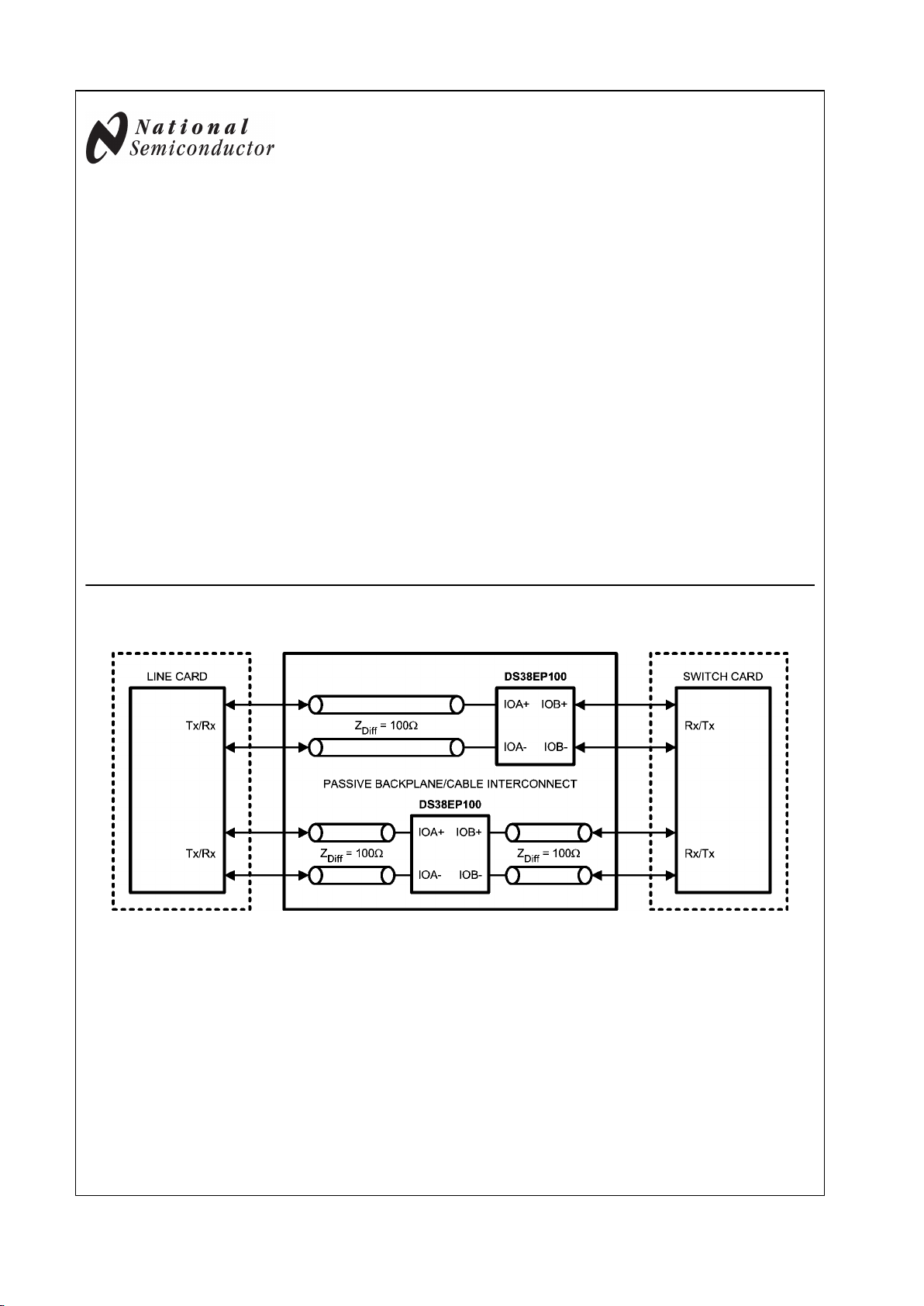
Simplified Application Diagram
30029201
Note:
The DS38EP100 provides the flexibility of passing the data from either side of the device. It can be placed anywhere in the data path..
© 2007 National Semiconductor Corporation 300292 www.national.com
DS38EP100 1 to 5 Gbps, Power-Saver Equalizer for Backplanes and Cables
Pin Descriptions
Pin Name Pin Number I/O, Type Description
High Speed Differential I/O
IOAIOA+
3
1
I/O Symmetric
differential I/O.
IOBIOB+
4
6
I/O Symmetric
differential I/O.
NC
Exposed
Pad
2, 5
DAP
N/A Reserved.
Do not connect.
Note:
I = Input / O = Output
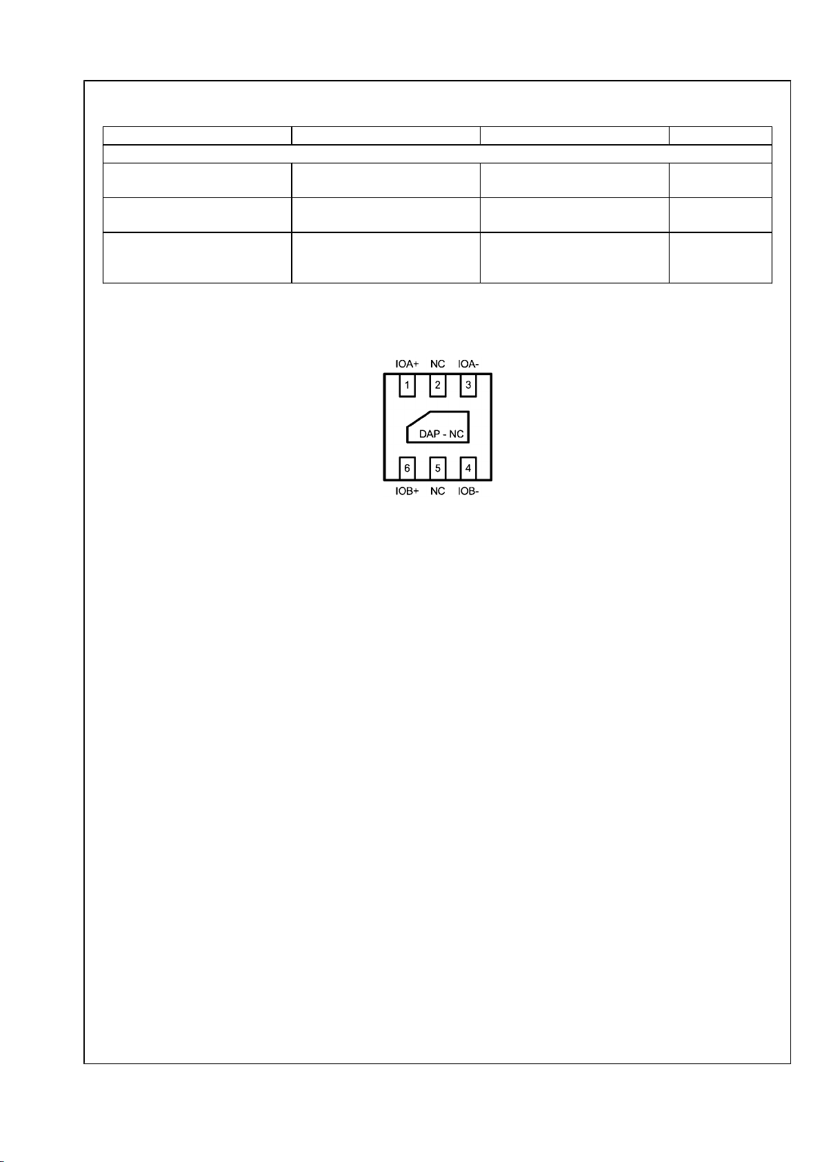
Pin Diagram
30029205
Bottom View shown
2.2mm x 2.5mm 6-Pin LLP Package
Order number DS38EP100
www.national.com 2
DS38EP100
Absolute Maximum Ratings (Note 1)
If Military/Aerospace specified devices are required,
please contact the National Semiconductor Sales Office/
Distributors for availability and specifications.
INPUT/OUTPUT
(IOA+ and IOB+) or (IOA- and IOB-) +2V
(IOA+ and IOA-) or (IOB+ and IOB-) +4V
(IOA+ and IOB-) or (IOA- and IOB+) +4V
Junction Temperature +150°C
Storage Temperature −65°C to +150°C
Lead Temperature
Soldering, 4 sec +260°C
ESD Rating
HBM, 1.5 kΩ, 100 pF 1.3kV
Recommended Operating
Conditions
Min Typ Max Units
Operating Temperature −40 25 +85 °C
Bit Rate 1 5 Gbps
Electrical Characteristics (Note 6) Over recommended operating conditions unless other specified. All
parameters are guaranteed by test, statistical analysis or design.
Symbol Parameter Conditions Min
Typ
(Note 2)
Max Units
V
IN
Input voltage swing See (Note 3)
1000 3600 mVp-p
Equalization 2.5 GHz relative to 100MHz 6 dB
R
LI
Differential input return
loss
100 MHz – 2.5 GHz, with fixture's effect deembedded
15 dB
R
LO
Differential output
return loss
100 MHz – 2.5 GHz, with fixture's effect deembedded. IOA+,or IOB+ = static high.
15 dB
R
IN
Input Impedance
Differential across IOA+ and IOA-, or IOB+ and
IOB-, ZLOAD = 100Ω
100
Ω
R
O
Output Impedance
Differential across IOA+ and IOA-, or IOB+ and
IOB-, ZSOURCE = 100Ω
100
Ω
Through Response Relative to ideal load, see Figure 2 for setup See Figure 3 and Table 1 for limits
R1
Resistance IOA+ to
IOA- and IOB+ to IOB- No load, high impedance on all ports
150
Ω
R2
Resistance IOA+ to
IOB+ and IOA- to IOB- No load, high impedance on all ports
50
Ω
R3
Resistance IOA+ to
IOB- and IOA- to IOB+ No load, high impedance on all ports
150
Ω
DC Gain
Z
LOAD = 100Ω
0.4
(IOA/IOB or IOB/IOA)
DJ1
Residual deterministic
jitter
2.5 Gbps, 40 in of 6mil microstrip FR4
0.1 UIp-p
See (Note 4)
DJ2
Residual deterministic
jitter
3.125 Gbps, 40 in of 6mil microstrip FR4
0.1 0.15 UIp-p
See (Notes 4, 5)
DJ3
Residual deterministic
jitter
3.8 Gbps, 40 in of 6mil microstrip FR4
0.1 0.15 UIp-p
See (Notes 4, 5)
DJ4
Residual deterministic
jitter
5 Gbps, 30 in of 6mil microstrip FR4
0.1 UIp-p
See (Note 4)
3 www.national.com
DS38EP100

Note 1: “Absolute Maximum Ratings” indicate limits beyond which damage to the device may occur, including inoperability and degradation of device reliability
and/or performance. Functional operation of the device and/or non-degradation at the Absolute Maximum Ratings or other conditions beyond those indicated in
the Recommended Operating Conditions is not implied. The Recommended Operating Conditions indicate conditions at which the device is functional and the
device should not be operated beyond such conditions.
Note 2: Typical values represent most likely parametric norms, TA = +25 degC, and at the Recommended Operating Conditions at the time of product
characterization and are not guaranteed.
Note 3: Differential signal to Equalizer, measured at the input to a transmission line, see point A of Figure 1. The transmission line is Z0 = 100Ω, 6-mil, microstrip
in FR4 material.
Note 4: Deterministic jitter is measured at the differential outputs (point C of Figure 1), minus the deterministic jitter before the test channel (point A of Figure 1).
Test pattern: PRBS- 7 .
Note 5: Specification is guaranteed by characterization and is not tested in production.
Note 6: The Electrical Characteristics tables list guaranteed specifications under the listed Recommended Operating Conditions except as otherwise modified
or specified by the Electrical Characteristics Conditions and/or Notes. Typical specifications are estimations only and are not guaranteed.
www.national.com 4
DS38EP100
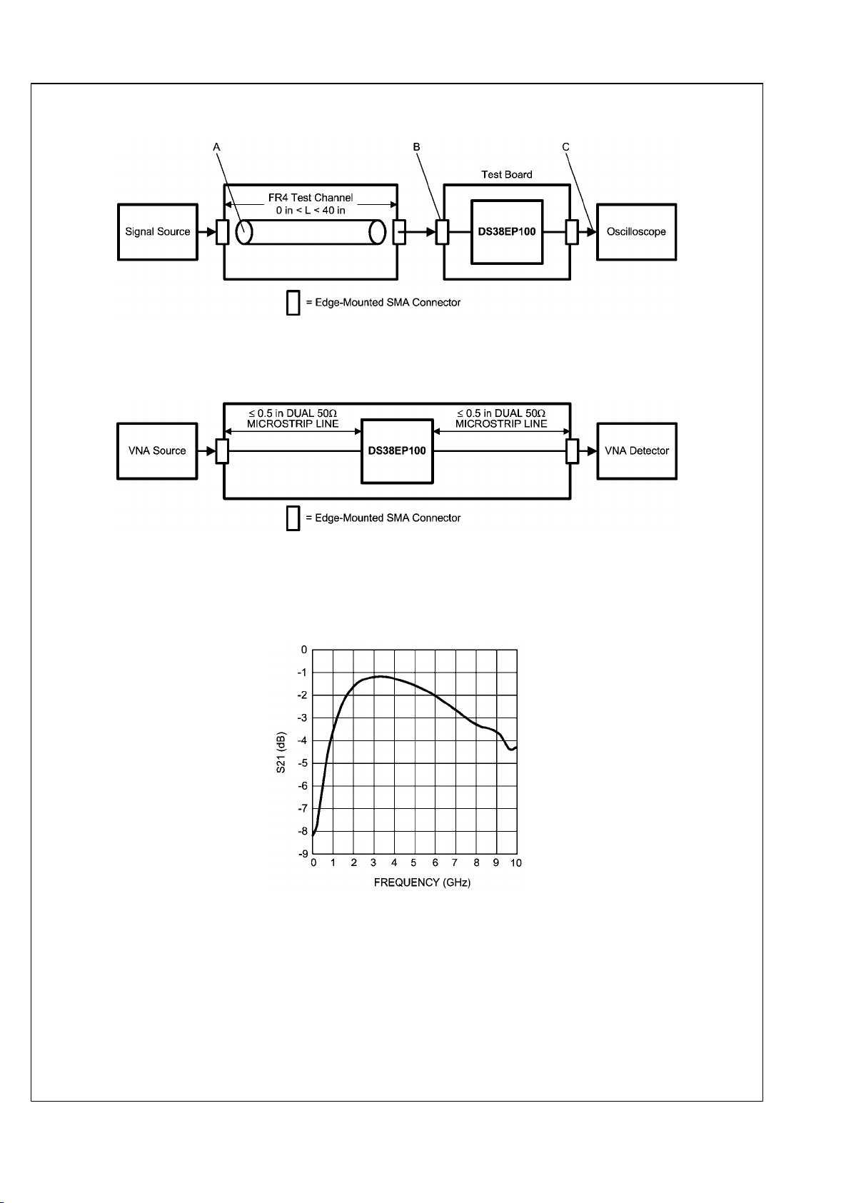
Test Setup Diagrams
30029203
FIGURE 1. Transient Test Setup Diagram
30029204
FIGURE 2. Frequency Response Test Circuit
Typical Equalizer Transfer Function
30029206
FIGURE 3. Typical Equalizer Transfer Function
5 www.national.com
DS38EP100
 Loading...