

NSC DS3886AVX, DS3886AVF, DS3886AV Datasheet

DS3886A
BTL 9-Bit Latching Data Transceiver
General Description
The DS3886A is a higher speed, lower power, pin compatible version of the DS3886.
The DS3886A is one in a series of transceivers designed
specifically for the implementation of high performance Futurebus+ and proprietary bus interfaces. The DS3886A is a
BTL 9-Bit Latching Data Transceiver designed to conform to
IEEE 1194.1(Backplane Transceiver Logic— BTL) as specified in the IEEE 896.2 Futurebus+ specification. The
DS3886A incorporates an edge-triggered latch in the driver
path which can be bypassed during fall-through mode of operation and a transparent latch in the receiver path. Utilization of the DS3886A simplifies the implementation of byte
wide address/data with parity lines and also may be used for
the Futurebus+ status, tag and command lines.
The DS3886A driver output configuration is an NPN open
collector which allows Wired-OR connection on the bus.
Each driver output incorporates a Schottky diode in series
with it’s collector to isolate the transistor output capacitance
from the bus, thus reducing the bus loading in the inactive
state. The combined output capacitance of the driver output
and receiver input is less than 5 pF.The driver also has high
sink current capability to comply with the bus loading requirements defined within IEEE 1194.1 BTL specification.
Backplane Transceiver Logic (BTL) is a signaling standard
that was invented and first introduced by National Semiconductor, then developed by the IEEE to enhance the performance of backplane buses. BTL compatible transceivers
feature low output capacitance drivers to minimize bus loading, a 1V nominal signal swing for reduced power consumption and receivers with precision thresholds for maximum
noise immunity. The BTL standard eliminates settling time
delays that severely limit TTL bus performance, and thus
provide significantly higher bus transfer rates. The backplane bus is intended to be operated with termination resistors (selected to match the bus impedance) connected to
2.1V at both ends. The low voltage is typically 1V.
Separate ground pins are provided for each BTL output to
minimize induced ground noise during simultaneous switching.
The unique driver circuitry meets the maximum slew rate of
0.5 V/ns which allows controlled rise and fall times to reduce
noise coupling to adjacent lines.
The transceiver’s high impedance control and driver inputs
are fully TTL compatible.
The receiver is a high speed comparator that utilizes a Bandgap reference for precision threshold control, allowing maximum noise immunity to the BTL 1V signaling level. Separate
QV
CC
and QGND pins are provided to minimize the effects
of high current switching noise. The output is TRI-STATE
®
and fully TTL compatible.
The DS3886A supports live insertion as defined in IEEE
896.2 through the LI (Live Insertion) pin. To implement live
insertion the LI pin should be connected to the live insertion
power connector. If this function is not supported, the LI pin
must be tied to the V
CC
pin. The DS3886A also provides
glitch free power up/down protection during power sequencing.
The DS3886A has two types of power connections in addition to the LI pin. They are the Logic V
CC(VCC
) and the Quiet
V
CC
(QVCC). There are two Logic VCCpins on the DS3886A
that provide the supply voltage for the logic and control circuitry. Multiple connections are provided to reduce the effects of package inductance and thereby minimize switching
noise. As these pins are common to the V
CC
bus internal to
the device, a voltage delta should never exist between these
pins and the voltage difference between V
CC
and QV
CC
should never exceed±0.5V because of ESD circuitry.
When CD (Chip Disable) is high, An is in high impedance
state and Bn is high. To transmit data (An to Bn) the T/R signal is high.
When RBYP is high, the positive edge triggered flip-flop is in
the transparent mode. When RBYP is low, the positive edge
of the ACLK signal clocks the data.
In addition, the ESD circuitry between the V
CC
pins and all
other pins except for BTL I/O’s and LI pins requires that any
voltage on these pins should not exceed the voltage on V
CC
+0.5V.
There are three different types of ground pins on the
DS3886A; the logic ground (GND), BTL grounds
(B0GND–B8GND) and the Bandgap reference ground
(QGND). All of these ground reference pins are isolated
within the chip to minimize the effects of high current switching transients. For optimum performance the QGND should
be returned to the connector through a quiet channel that
does not carry transient switching current. The GND and
B0GND–B8GND should be connected to the nearest backplane ground pin with the shortest possible path.
Since many different grounding schemes could be implemented and ESD circuitry exists on the DS3886A, it is important to note that any voltage difference between ground pins,
QGND, GND or B0GND–B8GND should not exceed
±
0.5V
including power up/down sequencing.
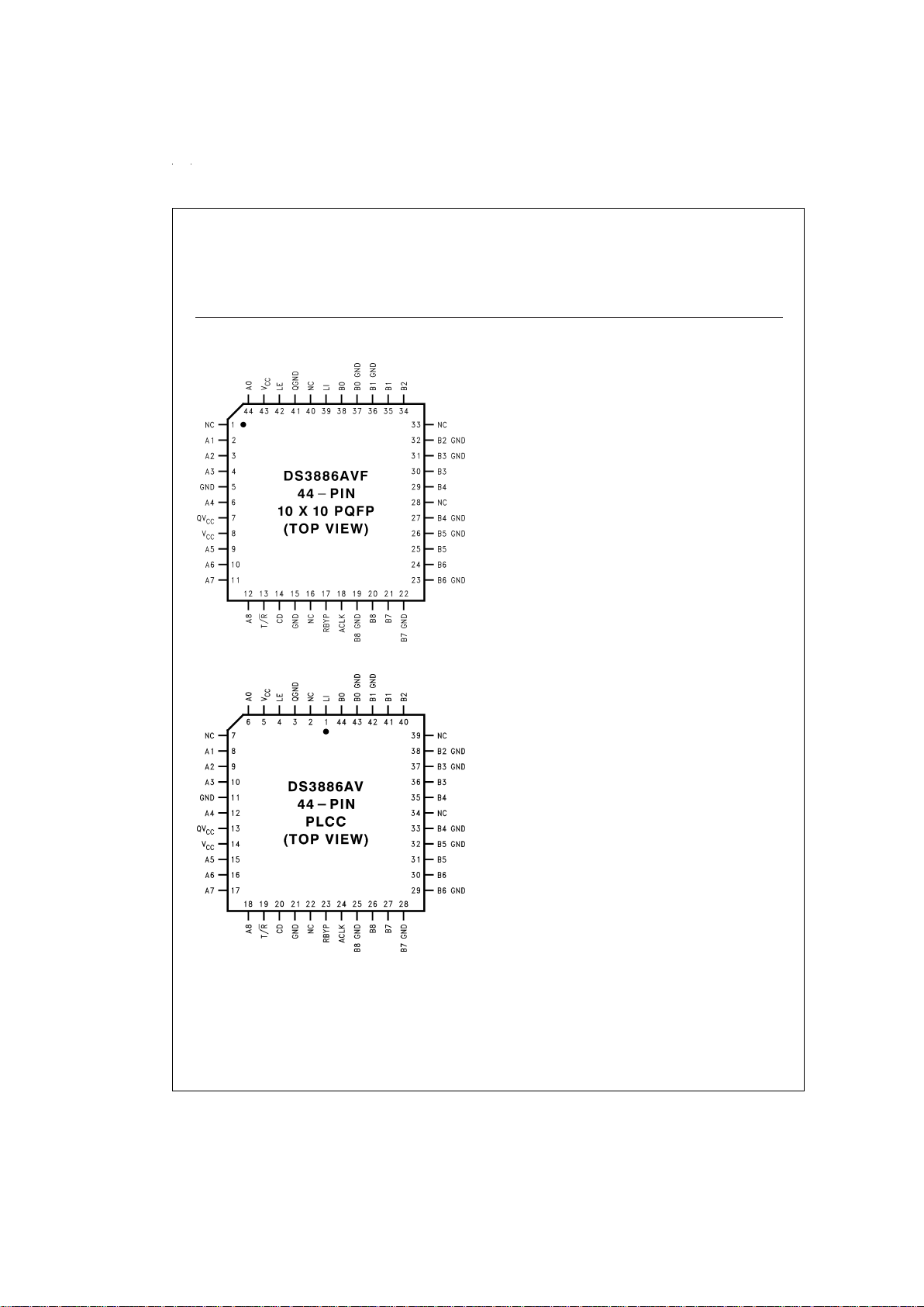
The DS3886A is offered in 44-pin PLCC, and 44-pin PQFP
high density package styles.
Features
n Fast propagation delay (3ns typ)
n 9-BIT BTL Latched Transceiver
n Driver incorporates edge triggered latches
n Receiver incorporates transparent latches
n Meets IEEE 1194.1 Standard on Backplane Transceiver
Logic (BTL)
n Supports Live Insertion
n Glitch free Power-up/down protection
n Typically less than 5 pF Bus-port capacitance
n Low Bus-port voltage swing (typically 1V) at 80 mA
TRI-STATE®is a registered trademark of National Semiconductor Corporation.
June 1998
DS3886A BTL 9-Bit Latching Data Transceiver
© 1999 National Semiconductor Corporation DS011458 www.national.com
Features (Continued)
n Exceeds 2 KV ESD testing (Human Body Model)
n Open collector Bus-port outputs allows Wired-OR
connection
n Controlled rise and fall time to reduce noise coupling to
adjacent lines
n TTL compatible Driver and Control inputs
n Built in Bandgap reference with separate QV
CC
and
QGND pins for precise receiver thresholds
n Individual Bus-port ground pins
n Product offered in PLCC and PQFP package styles
n Tight skew (0.5 ns typical)
Connection Diagrams
DS011458-1
DS011458-2
Order Number DS3886AV, or DS3886AVF
See NS Package Number V44A, or VF44B
www.national.com 2
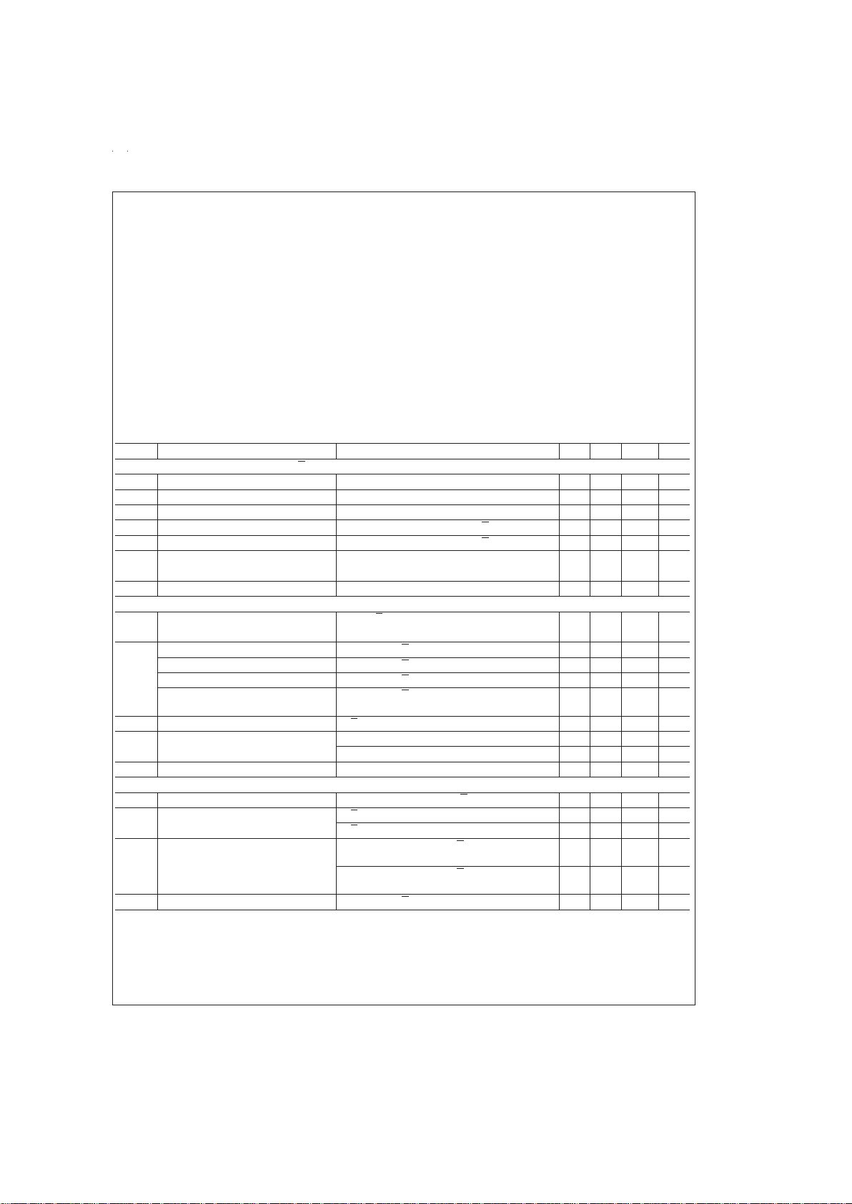
Absolute Maximum Ratings (Notes 1, 2)
If Military/Aerospace specified devices are required,
please contact the National Semiconductor Sales Office/
Distributors for availability and specifications.
Supply Voltage 6.5V
Control Input Voltage 6.5V
Driver Input and Receiver
Output 5.5V
Receiver Input Current
±
15 mA
Bus Termination Voltage 2.4V
Power Dissipation at 25˚C
PLCC (V44A) 2.5W
PQFP (VF44B) 1.3W
Derate PLCC Package (V44A) 20 mW/˚C
Derate PQFP Package
(VF44B) 11.1 mW/˚C
Storage Temperature Range −65˚C to +150˚C
Lead Temperature (Soldering, 4
sec.) 260˚C
Recommended Operating
Conditions
Min Max Units
Supply Voltage (V
CC
) 4.5 5.5 V
Bus Termination Voltage (V
T
) 2.06 2.14 V
Operating Free Air Temperature 0 70 ˚C
DC Electrical Characteristics (Notes 3, 4)
T
A
=
0˚ to +70˚C, V
CC
=
5V
±
10
%
Symbol Parameter Conditions Min Typ Max Units
DRIVER AND CONTROL INPUT (CD, T/R, An, ACLK, LE and RBYP)
V
IH
Minimum Input High Voltage 2.0 V
V
IL
Maximum Input Low Voltage 0.8 V
I
I
Input Leakage Current V
IN
=
V
CC
=
5.5V 250 µA
I
IH
Input High Current V
IN
=
2.4V, An=CD=0.5V, T/R=2.4V
40 µA
I
IL
Input Low Current V
IN
=
0.5V, An=CD=0.5V, T/R=2.4V
−10 µA
I
IL
Input Low Current An Port, An=0.5V, CD=0.5V −100 µA
T/R=2.4V, RBYp=2.4V
V
CL
Input Diode Clamp Voltage I
CLAMP
=
−12 mA −1.2 V
DRIVER OUTPUT/RECEIVER INPUT (Bn)
V
OLB
Output Low Bus Voltage An=T/R=2.4V, CD=0.5V, I
OL
=
80 mA
0.75 1.0 1.1 V
(Note 4)
I
OFF
Output Off Low Current An=0.5V, T/R=2.4V, Bn=0.75V, CD=0.5V −200 µA
Output Off High Current An=0.5V, T/R=2.4V, Bn=2.1V, CD=0.5V
200 µA
Output Off Low Current-Chip Disabled An=0.5V, T/R=CD=2.4V, Bn=0.75V
−50 µA
Output Off High Current-Chip
Disabled
An=0.5V, T/R=CD=2.4V, Bn=2.1V
50 µA
V
TH
Receiver Input Threshold T/R=CD=0.5V 1.47 1.55 1.62 V
V
CLP
Positive Clamp Voltage V
CC
=
Max or 0V, Bn=1 mA 2.4 3.4 4.5 V
V
CC
=
Max or 0V, Bn=10 mA 2.9 3.9 5.0 V
V
CLN
Negative Clamp Voltage I
CLAMP
=
−12 mA −1.2 V
RECEIVER OUTPUT (An)
V
OH
Voltage Output High Bn=1.1V, I
OH
=
−2mA, T/R=CD=0.5V
2.4 3.2 V
V
OL
Voltage Output Low T/R=CD=0.5V, Bn=2.1V, I
OL
=
24 mA
0.35 0.5 V
T/R=CD=0.5V, Bn=2.1V, I
OL
=
8mA
0.30 0.4 V
I
OZ
TRI-STATE Leakage Current V
IN
=
2.4V, CD=2.4V, T/R=0.5V,
Bn=0.75V
10 µA
V
IN
=
0.5V, CD=2.4V, T/R=0.5V,
Bn=0.75V
−10 µA
I
OS
Output Short Circuit Current Bn=1.1V, T/R=CD=0.5V (Note 3) −40 −70 −100 mA
www.national.com3
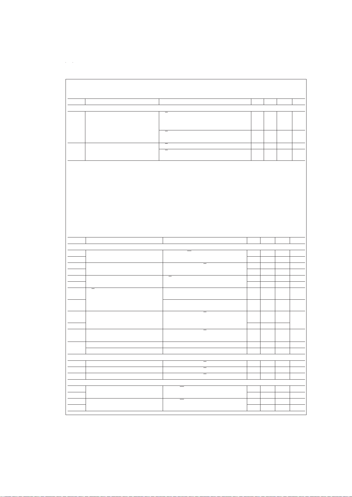
DC Electrical Characteristics (Notes 3, 4) (Continued)
T
A
=
0˚ to +70˚C, V
CC
=
5V
±
10
%
Symbol Parameter Conditions Min Typ Max Units
SUPPLY CURRENT
I
CCT
I
CCT
—Power Supply Current T/R=All An=3.4V, CD=0.5V
for a TTL High Input ACLK=LE=RBYP=3.4V 55 62 mA
(V
IN
=
V
CC
− 2.1V)
Supply Current: Sum of V
CC
, T/R=0.5V, All Bn=2.1V, LE=CD=0.5V 45 53 mA
QV
CC
and LI ACLK=RBYP=3.4V
I
LI
Live Insertion Current T/R=An=CD=ACLK=0.5V 1.5 2.2 mA
T/R=All An=RBYB=2.4V,
CD=ACLK=0.5V
3 4.5 mA
Note 1: “Absolute maximum ratings” are those beyond which the safety of the device cannot be guaranteed. They are not meant to imply that the device should be
operated at these limits. The table of “Electrical Characteristics” provides conditions for actual device operation.
Note 2: All input and/or output pins shall not exceed V
CC
plus 0.5V and shall not exceed the absolute maximum rating at anytime, including power-up and power
down. This prevents the ESD structure from being damaged due to excessive currents flowing from the input and/or output pins to QV
CC
and VCC. There is a diode
between each input and/or output to V
CC
which is forward biased when incorrect sequencing is applied. Alternatively, a current limiting resistor can be used when
pulling-up the inputs to prevent damage. The current into any input/output pin shall be no greater than 50 mA. Exception, LI and Bn pins do not have power sequencing requirements with respect to V
CC
and QVCC. Furthermore, the difference between VCCand QVCCshould never be greater than 0.5V at any time including
power-up.
Note 3: All currents into device pins are positive; all currents out of device pins are negative. All voltages are referenced to device ground unless otherwise specified.
All typical values are specified under these conditions: V
CC
=
5V and T
A
=
25˚C, unless otherwise stated.
Note 4: Only one output should be shorted at a time, and duration of the short should not exceed one second.
Note 5: Referenced to appropriate signal ground. Do not exceed maximum power dissipation of package.
AC Electrical Characteristics (Note 5)
T
A
=
0˚C to +70˚C, V
CC
=
5V
±
10
%
Symbol Parameter Conditions Min Typ Max Units
DRIVER
t
PHL
An to Bn Propagation Delay CD=0V, T/ R=RBYP=3V 135ns
t
PLH
Fall-through mode (
Figure 1
and
Figure 2
) 1.5 3 5 ns
t
PHL
ACLK to Bn Propagation Delay CD=RBYP=0V, T/R=3V 1.7 4 6.5 ns
t
PLH
Latch mode (
Figure 1
and
Figure 4
) 2 4 6.5 ns
t
PHL
CD to Bn Enable Time T/R=3V, An=3V 359ns
t
PLH
Disable Time (
Figure 1
and
Figure 3
) 2.5 5 6.7 ns
t
PHL
T/R to Bn Enable Time CD=0V (
Figure 10
and
Figure 11
),
RBYP=3V
91318ns
t
PLH
Disable Time CD=0V (
Figure 10
and
Figure 11
),
RBYP=3V
258ns
t
r
Transition Time-Rise/Fall CD=RBYP=0V, T/R=3V
(
Figure 1
and
Figure 3
) (Note 10)
1 2 3.5 ns
t
f
20%to 80
%
124
SR Slew Rate is calculated from CD=RBYP=0V, T/R=3V
0.85 0.5 V/ns
1.3V to 1.8V (
Figure 1
and
Figure 2
) (Note 10)
t
skew
ACLK to Bn Same Package (Note 7) 0.8 3 ns
An to Bn Same Package (Note 7) 0.8 3 ns
DRIVER TIMING REQUIREMENTS (
Figure 4
)
t
S
An to ACLK Set-up Time CD=RBYP=0V, T/R=3V 3ns
t
H
ACLK to An Hold Time CD=RBYP=0V, T/R=3V 1ns
t
pw
ACLK Pulse Width CD=RBYP=0V, T/R=3V 3ns
RECEIVER
t
PHL
Bn to An Propagation Delay CD=T/ R=0V, LE=3V 3 4.5 6 ns
t
PLH
Bypass Mode (
Figure 5
and
Figure 6
) 3 4.5 6.5 ns
t
PHL
LE to An Propagation Delay CD=T/ R=0V 3.5 5.5 10 ns
t
PLH
Latch Mode (
Figure 5
and
Figure 7
) 4.5 5.5 8.5 ns
www.national.com 4
 Loading...