

NSC DS3885VX, DS3885VF, DS3885V Datasheet
TL/F/10721
DS3885 BTL Arbitration Transceiver
January 1994
DS3885 BTL Arbitration Transceiver
General Description
The DS3885 is one in a series of transceivers designed specifically for the implementation of high performance Futurebus
a
and proprietary bus interfaces. The DS3885 Arbitration Transceiver is designed to conform to IEEE 1194.1
(Backplane Transceiver LogicÐBTL) as specified in the
IEEE 896.2 Futurebus
a
specification. The Arbitration
Transceiver incorporates the competition logic internally
which simplifies the implementation of a Futurebus
a
appli-
cation by minimizing the on board logic required.
The DS3885 driver output configuration is an NPN open collector which allows Wired-OR connection on the bus. Each
driver output incorporates a Schottky diode in series with its
collector to isolate the transistor output capacitance from
the bus thus reducing the bus loading in the inactive state.
The BTL drivers also have high sink current capability to
comply with the bus loading requirements defined within
IEEE 1194.1 BTL specification.
Backplane Transceiver Logic (BTL) is a signaling standard
that was invented and first introduced by National Semicon-
(Continued)
Features
Y
9-bit inverting BTL transceiver
Y
Meets IEEE 1194.1 standard on Backplane Transceiver
Logic (BTL)
Y
Includes on chip competition logic and parity checking
Y
Supports live insertion
Y
Glitch free power-up/down protection
Y
Typically less than 5 pF bus-port capacitance
Y
Low bus-port voltage swing (typically 1V) at 80 mA
Y
Open collector bus-port output allows Wired-OR
connection
Y
Exceeds 2 kV ESD testing (Human Body Model)
Y
Individual bus-port ground pins minimize ground bounce
Y
Controlled rise and fall time to reduce noise coupling to
adjacent lines
Y
TTL compatible driver and control inputs
Y
Built in bandgap reference with separate QVCCand
QGND pins for precise receiver thresholds
Y
Product offered in PLCC and PQFP package styles
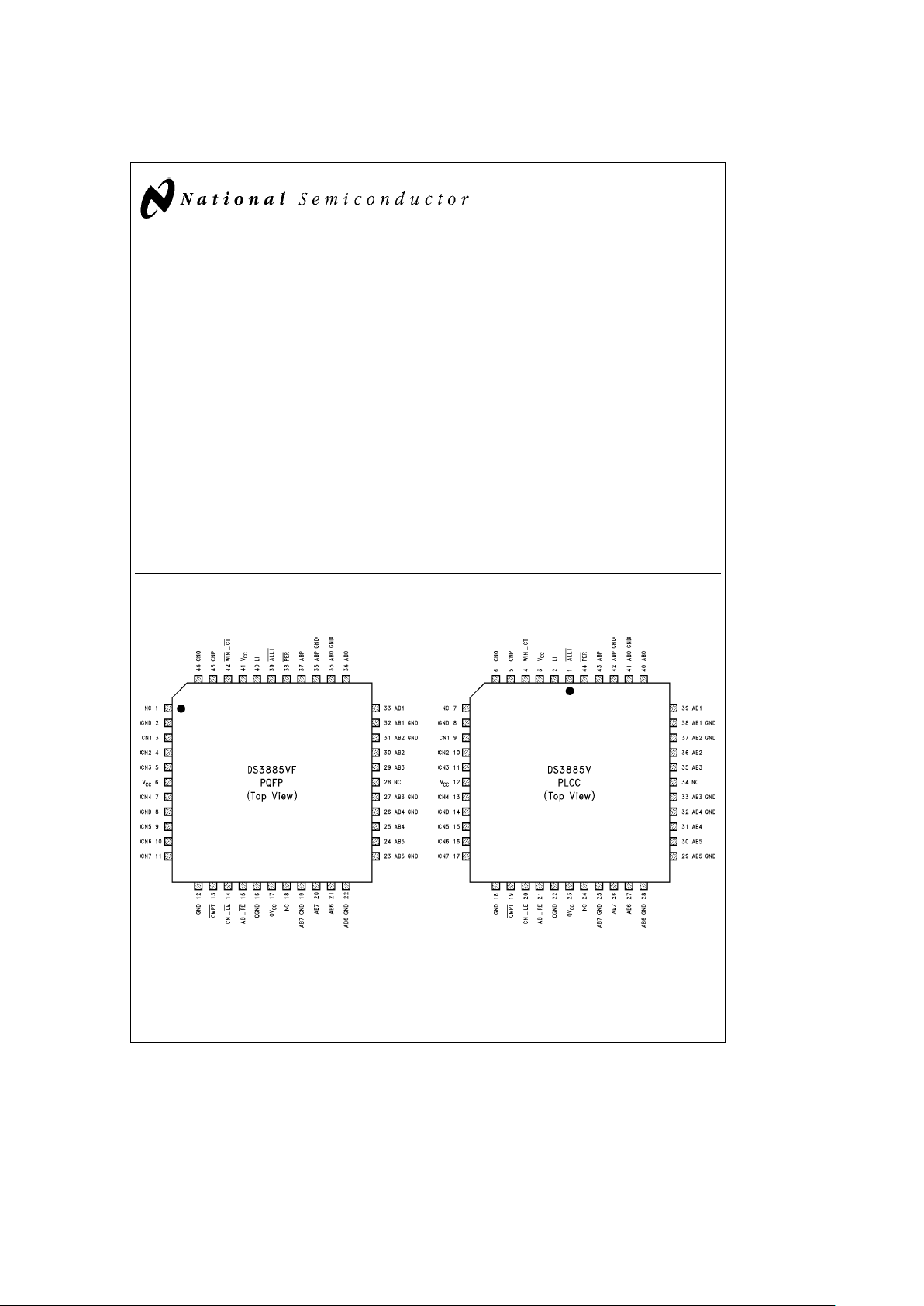
Connection Diagrams
TL/F/10721– 2 TL/F/10721– 13
Order Number DS3885V or DS3885VF
See NS Package Number V44A or VF44B
TRI-STATEÉis a registered trademark of National Semiconductor Corporation.
C
1995 National Semiconductor Corporation RRD-B30M75/Printed in U. S. A.

General Description (Continued)
ductor, then developed by the IEEE to enhance the performance of backplane buses. BTL compatible transceivers
feature low output capacitance drivers to minimize bus loading, a 1V nominal signal swing for reduced power consumption and receivers with precision thresholds for maximum
noise immunity. BTL eliminates settling time delays that severely limit TTL bus performance, and thus provide significantly higher bus transfer rates. The backplane bus is intended to be operated with termination resistors (selected
to match the bus impedance) connected to 2.1V at both
ends. The low voltage is typically 1V.
Separate ground pins are provided for each BTL output to
minimize induced ground noise during simultaneous switching.
The transceiver’s control and driver inputs are designed
with high impedance PNP input structures and are fully TTL
compatible.
The receiver is a high speed comparator that utilizes a
bandgap reference for precision threshold control allowing
maximum noise immunity to the BTL 1V signaling level.
Separate QV
CC
and QGND pins are provided to minimize
the effects of high current switching noise. The output is
TRI-STATE
É
and fully TTL compatible.
The signals abk7:0ldesignate the arbitration bus number
which this transceiver places on the bus. The signal names
AB
k
7:0ldesignate the open collector Wired-OR signals
on the backplane bus.
The DS3885 implements an odd parity check on the arbitration bus bits AB
k
7:0l, with ABP being the parity bit. The
signal PER
will indicate the parity check result. For a quick
indication of current bus conditions, the bus status block
generates ALL1
(all asserted) status when all bits
(AB
k
7:0l) are asserted by any module. This signal is used
by the DS3875 Arbitration Controller to detect the Arbitration message number (during phase 1) or the powerfail message number (during phase 2).
To latch the arbitration number into the transceiver, it is
placed onto the CN
k
7:0lport, and the CNÐLE signal is
asserted. When the CMPT
signal is asserted, the arbitration
number is placed on the bus lines AB
k
7:0l. The WIN
Ð
GT
signal serves two purposes during the arbitration cycle. If
the CMPT
signal is not asserted during the arbitration cycle,
the transceiver compares its internally latched number to
the number on the AB
k
7:0lbus lines. If the internal number on the transceiver is greater than or equal to the number
on the AB
k
7:0llines, the WIN
Ð
GT
signal is asserted.
However, if the CMPT
signal is asserted, the transceiver
participates in the competition. If the transceiver wins the
arbitration, the WIN
Ð
GT
signal is asserted to confirm the
winning. The ABÐRE
signal is used to enable the on-chip
receiver outputs.
The DS3885 supports live insertion as defined in IEEE
896.2 through the LI (Live Insertion) pin. To implement live
insertion the LI pin should be connected to the live insertion
power connector. If this function is not supported the LI pin
must be tied to the V
CC
pin. The DS3885 also provides
glitch free power-up/down protection during power sequencing.
The DS3885 has two types of power connections in addition
to the LI pin. They are the Logic V
CC(VCC
) and the Quiet
V
CC
(QVCC). There are two VCCpins on the DS3885 that
provide the supply voltage for the logic and control circuitry.
Multiple power pins reduce the effects of package inductance and thereby minimize switching noise. As these pins
are common to the V
CC
bus internal to the device, a voltage
difference should never exist between these pins and the
voltage difference between V
CC
and QVCCshould never
exceed
g
0.5V because of ESD circuitry.
Additionally, the ESD circuitry between the V
CC
pins and all
other pins except for BTL I/O’s and LI pins requires that any
voltage on these pins should not exceed the voltage on V
CC
a
0.5V
There are three different types of ground pins on the
DS3885. They are the logic ground (GND), BTL grounds
(AB0GND–AB7GND/ABPGND) and the Bandgap reference ground (QGND). All of these reference pins are isolated within the chip to minimize the effects of high current
switching transients. For optimum performance the QGND
should be returned to the connector through a quiet channel
that does not carry transient switching current. The GND
and AB0GND – AB7GND/ABPGND should be connected to
the nearest backplane ground pin with the shortest possible
path.
Since many different grounding schemes could be implemented and ESD circuitry exists on the DS3885, it is important to note that any voltage difference between ground
pins, QGND, GND or AB0GND –AB7GND and ABPGND
should not exceed
g
0.5V including power-up/down se-
quencing.
Three additional transceivers are included in the Futurebus
a
family. They are the DS3883A BTL 9-bit Transceiver.
The DS3884A BTL Handshake Transceiver features selectable Wired-OR glitch filtering. The DS3886A BTL 9-bit
Latching Data Transceiver contains edge triggered latches
in the driver which may be bypassed during a fall-through
mode. In addition, the device contains a transparent latch in
the receiver section.
The DS3875 Arbitration Controller included in the Futurebus
a
family supports all the required and optional modes
for Futurebus
a
arbitration protocol. It is designed to be
used in conjunction with the DS3884A and DS3885 transceivers.
The LOGICAL INTERFACE FUTUREBUS
a
ENGINE (LIFE)
is a high performance Futurebus
a
Protocol Controller designed for IEEE 896.1. The LIFE will handle all handshaking
signals between the Futurebus
a
and the local bus inter-
face. The Protocol Controller supports the Futurebus
a
compelled mode data transfer as both master and slave.
The Protocol Controller can be configured to operate in
compliance to IEEE 896.2 Profile B mode. The LIFE incorporates a DMA controller and 64-bit FIFO’s for fast queuing.
All of the transceivers are offered in 44-pin PLCC and PQFP
high density package styles.
2
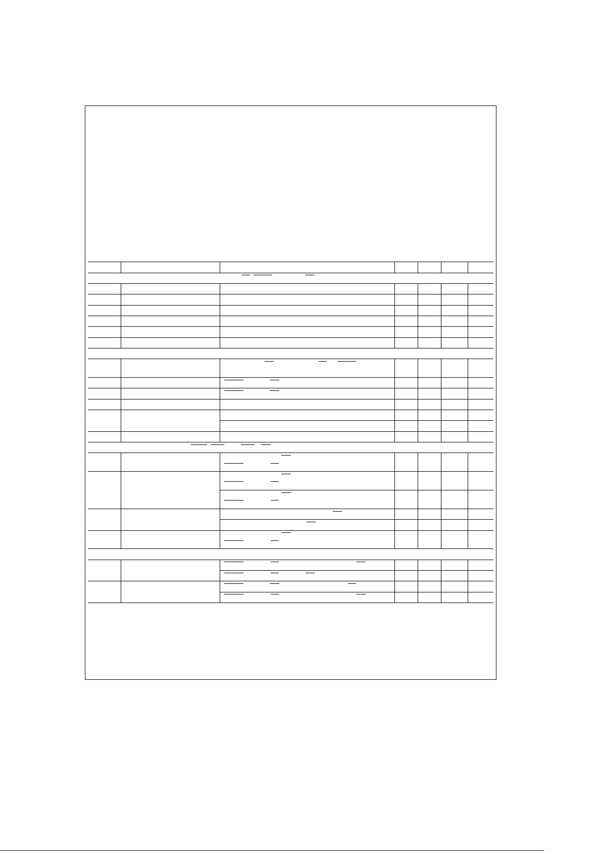
Absolute Maximum Ratings (Notes 1 and 2)
If Military/Aerospace specified devices are required,
please contact the National Semiconductor Sales
Office/Distributors for availability and specifications.
Supply Voltage 6.5V
Control Input Voltage 6.5V
Driver Input and Receiver Output 5.5V
Receiver Input Current
g
15 mA
Bus Termination Voltage 2.4V
Power Dissipation at 25§C PLCC 2.5W
PQFP 1.3W
Derate PLCC Package 20 mW/
§
C
Derate PQFP Package 11.1 mW/
§
C
Storage Temperature Range
b
65§Ctoa150§C
Lead Temperature (Soldering, 4 sec.) 260§C
Recommended
Operating Conditions
Min Max Units
Supply Voltage, V
CC
4.5 5.5 V
Bus Termination Voltage (VT) 2.06 2.14 V
Operating Free Air Temperature 0 70
§
C
DC Electrical Characteristics (Notes 2 and 3) T
A
e
0§Ctoa70§C, V
CC
e
5Vg10%
Symbol Parameter Conditions Min Typ Max Units
DRIVER AND CONTROL INPUT (CNn CNP, CNÐLE, CMPT, and ABÐRE)
V
IH
Minimum Input High Voltage 2.0 V
V
IL
Maximum Input Low Voltage 0.8 V
I
I
Input Leakage Current V
IN
e
V
CC
e
5.5V 100 mA
I
IH
Input High Current V
IN
e
2.4V 40 mA
I
IL
Input Low Current V
IN
e
0.5V
b
100 mA
V
CL
Input Diode Clamp Voltage I
CLAMP
eb
12 mA
b
1.2 V
DRIVER OUTPUT/RECEIVER INPUT (ABn and ABP)
V
OLB
Output Low Bus Voltage CNneABÐREe2.4V, CNÐLEeCMPTe0.5V
0.75 1.0 1.1 V
(Note 5) I
OL
e
80 mA
I
OLBZ
Output Low Bus Current CMPTeABÐREe2.4V, ABne0.75V
b
100 mA
I
OHBZ
Output High Bus Current CMPTeABÐREe2.4V, ABne2.1V 100 mA
V
TH
Receiver Input Threshold 1.47 1.55 1.62 V
V
CLP
Positive Clamp Voltage V
CC
e
Max or 0V, I
ABn
e
1 mA 2.4 3.4 4.5 V
V
CC
e
Max or 0V, I
ABn
e
10 mA 2.9 3.9 5.0 V
V
CLN
Negative Clamp Voltage I
CLAMP
eb
12 mA
b
1.2 V
RECEIVER OUTPUT (CNn, CNP, ALL1, PER, and WIN
Ð
GT
)
V
OH
Voltage Output High ABne1.1V, ABÐREe0.5V,
2.4 3.2 V
CMPT
e
CNÐLEe2.4V, I
OH
eb
2mA
V
OL
Voltage Output Low ABne2.1V, ABÐREe0.5V,
0.35 0.5 V
CMPT
e
CNÐLEe2.4V, I
OL
e
24 mA
ABne2.1V, ABÐREe0.5V,
0.30 0.4 V
CMPT
e
CNÐLEe2.4V, I
OL
e
8mA
I
OZ
TRI-STATE Leakge Current CNneCNPe2.4V,e2.4V, ABÐREe2.4V 40 mA
CNneCNPe0.5V, ABÐREe2.4V
b
100 mA
I
OS
Output Short Circuit Current ABne1.1V, ABÐREe0.5V
b40b70b
100 mA
CMPT
e
CNÐLEe2.4V (Note 4)
SUPPLY CURRENT
I
CC
Supply Current: Includes VCC, CMPTeCNÐLEe0.5V, All CNneABÐREe2.4V 75 100 mA
QVCCand LI
CMPT
e
CNÐLEeABÐREe2.4V 26 40 mA
I
LI
Live Insertion Current CMPTeABÐREeCNne2.4V, CNÐLEe0.5V 1.5 3 mA
CMPTeCNÐLEe0.5V, All CNneABÐREe2.4 3 5 mA
3
DC Electrical Characteristics (Notes 2 and 3) T
A
e
0§Ctoa70§C, V
CC
e
5Vg10% (Continued)
Note 1: Absolute Maximum Ratings are those beyond which the safety of the device cannot be guaranteed. They are not meant to imply that the device should be
operated at these limits. The tables of ‘‘Electrical Characteristics’’ provide conditions for actual device operation.
Note 2: All input and/or output pins shall not exceed V
CC
a
0.5V and shall not exceed the absolute maximum rating at any time, including power-up and power-
down. This prevents the ESD structure from being damaged due to excessive currents flowing from the input and/or output pins to QV
CC
and VCC. There is a diode
between each input and/or output to V
CC
which is forward biased when incorrect sequencing is applied. LI and Bn pins do not have power sequencing
requirements with respect to V
CC
and QVCC.
Note 3: All currents into device pins are positive; all currents out of device pins are negative. All voltages are referenced to device ground unless otherwise
specified. All typical values are specified under these conditions: V
CC
e
5V and T
A
e
25§C, unless otherwise stated.
Note 4: Only one output should be shorted at a time, and duration of the short not to exceed one second.
Note 5: Referenced to appropriate signal ground. Do not exceed maximum power dissipation of package.
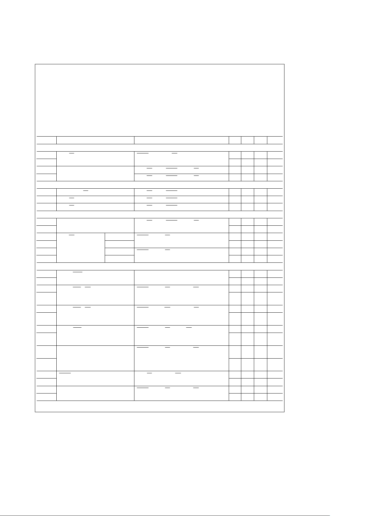
AC Electrical Characteristics T
A
e
0§Ctoa70§C, V
CC
e
5Vg10% (Note 6)
Symbol Parameter Conditions Min Typ Max Units
DRIVER (
Figures 1
and2)
t
PHL
CNÐLE to AB7 Propagation Delay CMPTe0V, ABÐREe3V 7 13 18 ns
t
PLH
61017 ns
trTransition TimeÐRise/Fall ABÐREe3V, CMPTeCNÐLEe03ns
t
f
20% to 80%
ABÐREe3V, CMPTeCNÐLEe01ns
DRIVER TIMING REQUIREMENTS (
Figures 1
and2)
t
S
CNn to CNÐLE Set-Up Time ABÐREe3V, CMPTe0V 9 ns
t
H
CNÐLE to CNn Hold Time ABÐREe3V, CMPTe0V 0 ns
t
PW
CNÐLE Pulse Width ABÐREe3V, CMPTe0V 15 ns
RECEIVER
t
PHL
ABn to CNn Propagation Delay ABÐREe0V, CMPTeCNÐLEe3V 5 13 22 ns
t
PLH
(
Figures 4
and5)
31523 ns
t
PLZ
ABÐRE to CNn Disable Time CMPTeCNÐLEe3V, ABne2.1V 3 6 11 ns
t
PZL
Enable Time
(
Figures 6
and7)
5 9 13 ns
t
PHZ
Disable Time CMPTeCNÐLEe3V, ABne1.1V 4 7 12 ns
t
PZH
Enable Time
(
Figures 6
and7)
3 6 11 ns
OTHERS
t
PHL
AB0 to ALL1 Propagation Delay ABk7:1
l
e
1.1V 7 16 28 ns
t
PLH
All Asserted Condition (
Figures 4
and8)
71626 ns
t
PHL
AB0 to WIN
Ð
GT
Propagation Delay CMPTeCNÐLEe0V, ABÐREe3V, 6 14 23 ns
t
PLH
Win Condition CNk7:0
l
e
0V
61423 ns
AB
k
7:0
l
e
2.1V (
Figures 4
and9)
t
PHL
AB0 to WIN
Ð
GT
Propagation Delay CMPTeABÐREe3V, CNÐLEe0V, 6 16 27 ns
t
PLH
Greater Than Condition CNk7:1
l
e
0V, CN0e3V
61626 ns
AB
k
7:0
l
e
2.1V (
Figures 4
and9)
t
PHL
ABP to PER Propagation Delay CMPTeCNÐLEeABÐREe3V, 6 13 23 ns
t
PLH
Parity Error Condition ABk7:1
l
e
1.1V, AB0e2.1V
41323 ns
(
Figures 4
and8)
t
PHL
ABn to ABknb1lPropagation Delay CMPTeCNÐLEe0V, ABÐREe3V,
51222 ns
CNne0V, CNknb1
l
e
3V,
t
PLH
CNk7:na1
l
e
0V, ABk7:na1
l
e
2.1V
51323 ns
(
Figures 1
and10)
t
PHL
CMPT to AB7 Propagation Delay CNÐLEe0V, ABÐREeCN7e3V 4 8 14 ns
t
PLH
(
Figures 1
and3)
5 9 16 ns
t
PHL
AB7 to ABP Propagation Delay CMPTeCNÐLEe0V, ABÐREeCNPe3V, 36 60 ns
t
PLH
CNk7:0
l
e
0V (
Figures 1
and10)
36 60 ns
4
 Loading...