

NSC DS3884AW-883, DS3884AVX, DS3884AVF, DS3884AV Datasheet
DS3884A
BTL Handshake Transceiver
General Description
The DS3884A is one in a series of transceivers designed
specifically for the implementation of high performance Futurebus+ and proprietary bus interfaces. The DS3884A is a
BTL 6-bit Handshake Transceiver designed to conform to
IEEE 1194.1 (Backplane Transceiver Logic—BTL) as specified in the IEEE 896.2 Futurebus+ specification.
Features
n Fast propagation delay (3 ns typ)
n 6-bit BTL transceiver
n Selective receiver glitch filtering (FR1–FR3)
n Meets 1194.1 Standard on Backplane Transceiver Logic
(BTL)
n Supports live insertion
n Glitch free power-up/down protection
n Typically less than 5 pF bus-port capacitance
n Low Bus-port voltage swing (typically 1V) at 80 mA
n TTL compatible driver and control inputs
n Separate TTL I/O
n Open collector bus-port outputs allow Wired-OR
connection
n Controlled rise and fall time to reduce noise coupling to
adjacent lines
n Built in Bandgap reference with separate QV
CC
and
QGND pins for precise receiver thresholds
n Exceeds 2 kV ESD testing (Human Body Model)
n Individual Bus-port ground pins
n Product offered in PQFP package styles
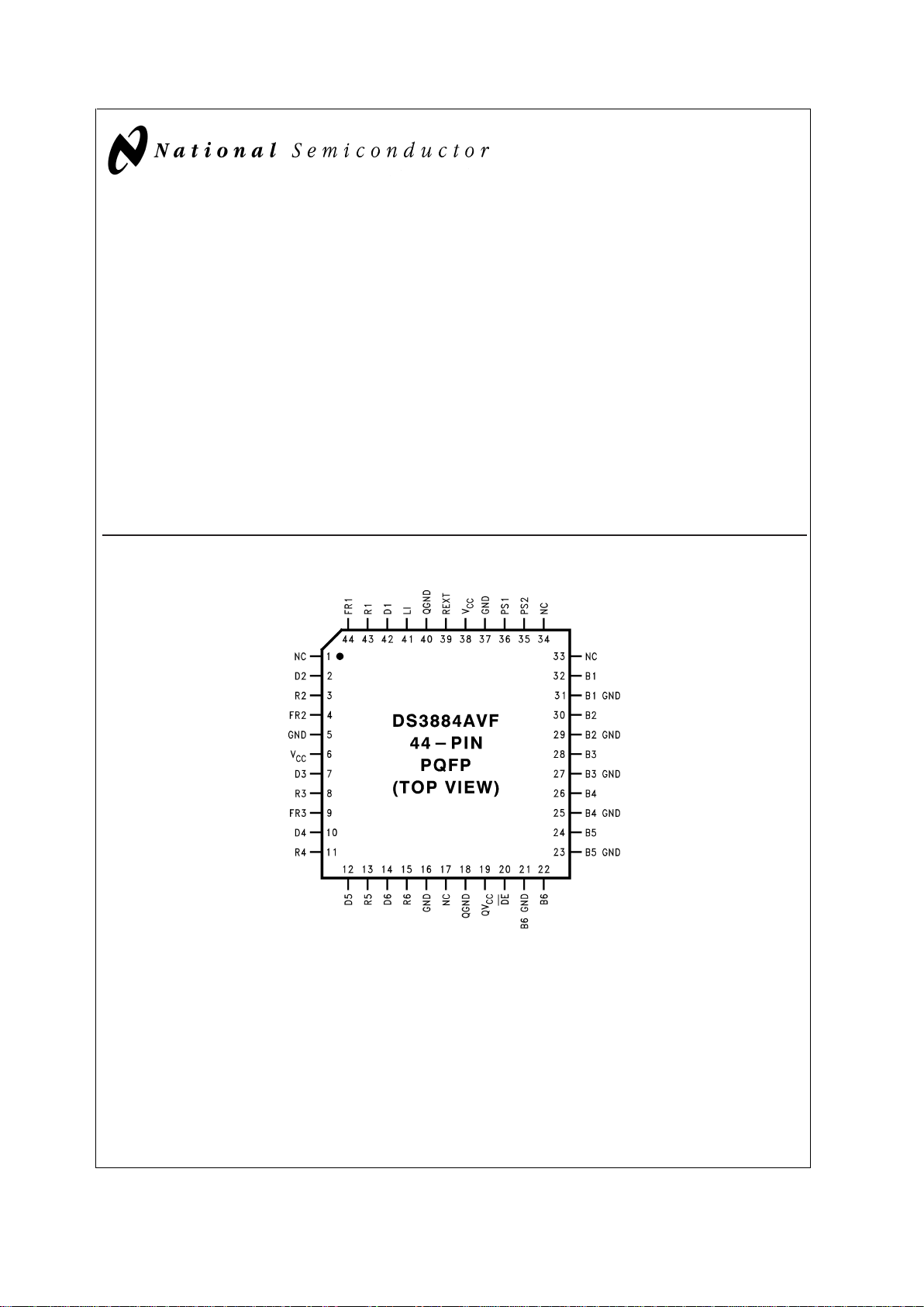
Connection Diagram
TRI-STATE®is a registered trademark of National Semiconductor Corporation.
DS011460-1
Order Number DS3884AVF
See NS Package VF44B
August 2000
DS3884A BTL Handshake Transceiver
© 2000 National Semiconductor Corporation DS011460 www.national.com

Logic Diagram
DS011460-3
DS3884A
www.national.com 2
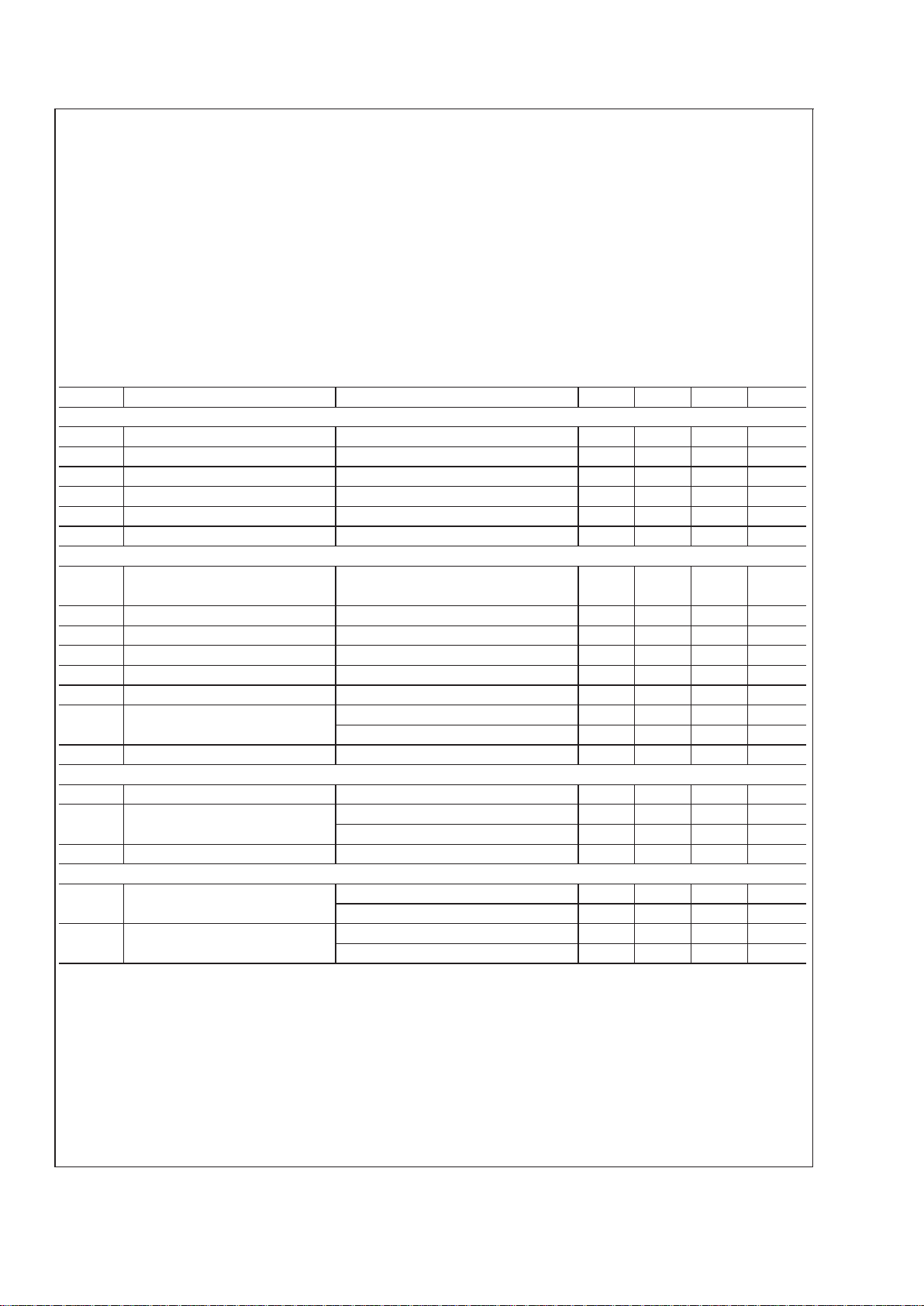
Absolute Maximum Ratings (Note 1)
If Military/Aerospace specified devices are required,
please contact the National Semiconductor Sales Office/
Distributors for availability and specifications.
Supply Voltage 6.5V
Control Input Voltage 6.5V
Driver Input and Receiver Output 5.5V
Receiver Input Current
±
15 mA
Bus Termination Voltage 2.4V
Power Dissipation at 25˚C
PQFP 1.3W
Derate PQFP Package 11.1 mW/˚C
Storage Temperature Range −65˚C to +150˚C
Lead Temperature
(Soldering, 4 seconds): 260˚C
Recommended Operating
Conditions
Supply Voltage, V
CC
4.5V–5.5V
Bus Termination Voltage (V
T
) 2.06V–2.14V
Operating Free Air Temperature 0˚C to 70˚C
DC Electrical Characteristics (Notes 2, 3)
TA= 0 to +70˚C, VCC=5V±10%
Symbol Parameter Conditions Min Typ Max Units
DRIVER AND CONTROL INPUT: (Dn, DE
*
, PS1 and PS2)
V
IH
Minimum Input High Voltage 2.0 V
V
IL
Maximum Input Low Voltage 0.8 V
I
I
Input Leakage Current VIN=VCC= 5.5V 100 µA
I
IH
Input High Current VIN= 2.4V 40 µA
I
IL
Input Low Current VIN= 0.5V −100 µA
V
CL
Input Diode Clamp Voltage I
CLAMP
= −12 mA −1.2 V
DRIVER OUTPUT/RECEIVER INPUT: (Bn)
V
OLB
Output Low Bus Voltage Dn = 2.4V, DE*= 0V, 0.75 1.0 1.1 V
(Note 5) I
OL
=80mA
I
OLBZ
Output Low Bus Current Dn = 0.5V, DE*= 2.4V, Bn = 0.75V 100 µA
I
OHBZ
Output High Bus Current Dn = 0.5V, DE*= 2.4V, Bn = 2.1V 100 µA
I
OLB
Output Low Bus Current Dn = 0.5V, DE*= 0V, Bn = 0.75V 220 µA
I
OHB
Output High Bus Current Dn = 0.5V, DE*= 0V, Bn = 2.1V 350 µA
V
TH
Receiver Input Threshold DE*= 2.4V 1.47 1.55 1.62 V
V
CLP
Positive Clamp Voltage VCC= Max or 0V, IBn= 1 mA 2.4 3.4 4.5 V
V
CC
= Max or 0V, IBn= 10 mA 2.9 3.9 5.0 V
V
CLN
Negative Clamp Voltage I
CLAMP
= −12 mA −1.2 V
RECEIVER OUTPUT: (FRn and Rn)
V
OH
Voltage Output High Bn = 1.1V, DE*= 2.4V, IOH= −2 mA 2.4 3.2 V
V
OL
Voltage Output Low Bn = 2.1V, DE*= 2.4V, IOL= 24 mA 0.35 0.5 V
Bn = 2.1V, DE
*
= 2.4V, IOL= 8 mA 0.35 0.4 V
I
OS
Output Short Circuit Current Bn = 1.1V, DE*= 2.4V (Note 4) −40 −70 −100 mA
SUPPLY CURRENT
I
CC
Supply Current: Includes VCC,DE
*
= 0.5V, All Dn = 2.4V 50 70 mA
QV
CC
and LI DE*= 2.4V, All Bn = 2.1V 50 70 mA
I
LI
Live Insertion Current DE*= 2.4V, All Dn = 0.5V 1 3 mA
DE
*
= 0.5V, All Dn = 2.4V 2 5 mA
Note 1: “Absolute Maximum Ratings” are those beyond which the safety of the device cannot be guaranteed. They are not meant to imply that the device should
be operated at these limits. The table of “Electrical Characteristics” provide conditions for actual device operation.
Note 2: All input and/or output pins shall not exceed V
CC
plus 0.5V and shall not exceed the absolute maximum rating at anytime, including power-up and
power-down. This prevents the ESD structure from being damaged due to excessive currents flowing from the input and/or output pins to QV
CC
and VCC. There is
a diode between each input and/or output to V
CC
which is forward biased when incorrect sequencing is applied. Alternatively, a current limiting resistor can be used
when pulling-up the inputs to prevent damage. The current into any input/output pin shall be no greater than 50 mA. Exception, LI and Bn pins do not have power
sequencing requirementswith respect to V
CC
and QVCC. Furthermore,the difference between VCCand QVCCshould neverbe greater than 0.5V atany time including
power-up.
Note 3: All currents intodevice pins are positive; all currents outof device pins are negative.All voltages are referenced to device groundunless otherwise specified.
All typical values are specified under these conditions.: V
CC
= 5V and TA= 25˚C unless otherwise stated.
Note 4: Only one output should be shorted at a time, and duration of the short should not exceed one second.
Note 5: Referenced to appropriate signal ground. Do not exceed maximum power dissipation of package.
DS3884A
www.national.com3
 Loading...