

TL/H/10747
DS3875 Futurebus
a
Arbitration Controller
November 1995
DS3875 FuturebusaArbitration Controller
General Description
The DS3875 FuturebusaArbitration Controller is a member
of National Semiconductor’s Futurebus
a
chip set designed
specifically for the IEEE 896.1 Futurebus
a
standard. The
DS3875 implements Distributed Arbitration and Distributed
Arbitration messages in a single chip.
The DS3875 interfaces with Futurebus
a
through the
DS3885 BTL Arbitration Transceiver and the DS3884A BTL
Handshake Transceiver. The DS3885 BTL Arbitration
Transceiver incorporates the competition logic needed for
the Arbitration Number signal lines. The DS3884A BTL
Handshake Transceiver has selectable Wired-OR receiver
glitch filtering. The DS3884A is used for the Arbitration Sequencing and Arbitration Condition signal lines.
Additional transceivers included in the Futurebus
a
chip set
are the DS3883A BTL 9-bit Data Transceiver and the
DS3886A BTL 9-bit Latching Data Transceiver. The
DS3886A transceiver features edge-triggered latches in the
driver which may be bypassed during a fall-through mode
and a transparent latch in the receiver. The DS3883A transceiver has no latches in either direction.
The Logical Interface Futurebus
a
Engine (LIFE) I/O Protocol Controller with 64-bit Data Path incorporates the Compelled Mode Futurebus
a
Parallel Protocol. The Protocol
Controller handles all the handshaking signals between the
Futurebus
a
and the local bus interfaces, and incorporates
a DMA Controller with built-in FIFOs for fast queueing.
Features
Y
The controller implements the complete requirements
of the IEEE 896.1 specification as a subset of its features
Y
Supports Arbitration message sending and receiving
Y
Supports the two modes of operation (RESTRICTED/
UNRESTRICTED)
Y
Software configurable double/single pass operation,
slow/fast, IBA/Parking and restricted/unrestricted
modes of arbitration
Y
Built-in 1 ms timer for use in the arbitration cycle
Y
User programmable 16 arbitration delays (8 slow and
8 fast)
Y
Built-in PLL for accurate delays. The PLL accepts
clocks from 2 MHz to 40 MHz in steps of 1 MHz
Y
Signal to unlock slave modules on transfer of tenure.
Auto unlock through a dummy cycle if the current master locked resources
Y
Programmable delay for releasing ar* after issuing
COMPETE/IBAÐCMPT. This is to ensure the assertion
of the arbitration number during competition, before the
release of ar*. Also this delay ensures there is sufficient time to assert the AD/DATA lines during Idle Bus
Arbitration before the release of ar*
Y
Read/Write facility with data acknowledge for the host
to load arbitration numbers, an arbitration message,
and control registers
Y
On chip parity generator unloads the host of the additional parity generation function
Y
Separate interrupts to indicate error occurrence and arbitration message received. Interrupts cleared on a register write. Error status is available in a separate status
register
Y
A special output pin to indicate that a POWERFAIL
message was received
Y
Hardwired register to hold the first word of the arbitration message
Y
FIFO strobe provided to store more than one arbitration
message externally to prevent overrun
Y
Idle Bus Arbitration (IBA) supported
Y
Parking implemented
Y
Bus initialization, system reset and Live-insertion supported. (The logic to detect these conditions must be
implemented externally.)
Y
Testability in the form of reading from key registers
which include the STATE, MCW, 1 ms timer and programmable input clock divider
TL/H/10747– 1
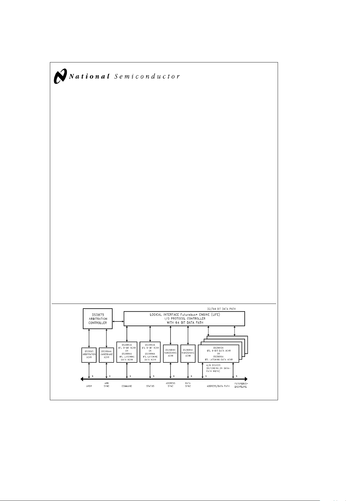
National’s FuturebusaChip Set Diagram
C
1995 National Semiconductor Corporation RRD-B30M115/Printed in U. S. A.

Table of Contents
1.0 INTRODUCTION TO FUTUREBUSaААААААААААААААААААААААААААААААААААААААААААААААААААААААААААААААААААААААААААА6
2.0 INTRODUCTION TO FUTUREBUS
a
ARBITRATION АААААААААААААААААААААААААААААААААААААААААААААААААААААААААААА6
2.1 The Arbitration States ААААААААААААААААААААААААААААААААААААААААААААААААААААААААААААААААААААААААААААААААААААААА7
3.0 INTRODUCTION TO DS3875 ARBITRATION CONTROLLER ААААААААААААААААААААААААААААААААААААААААААААААААААААА7
3.1 Using the DS3875 in 896.1 Compliant Mode ААААААААААААААААААААААААААААААААААААААААААААААААААААААААААААААААААА7
4.0 DS3875 INTERFACES ААААААААААААААААААААААААААААААААААААААААААААААААААААААААААААААААААААААААААААААААААААААА10
5.0 ARBITRATING FOR FUTUREBUS
a
АААААААААААААААААААААААААААААААААААААААААААААААААААААААААААААААААААААААААА12
5.1 Unrestricted/Restricted Modes of Operation АААААААААААААААААААААААААААААААААААААААААААААААААААААААААААААААААА12
5.2 The Arbitration Number and Arbitration Circuit ААААААААААААААААААААААААААААААААААААААААААААААААААААААААААААААААА12
5.2.1 Priority Field (PR)ААААААААААААААААААААААААААААААААААААААААААААААААААААААААААААААААААААААААААААААААААААА14
5.2.2 Round Robin Field (RR) ААААААААААААААААААААААААААААААААААААААААААААААААААААААААААААААААААААААААААААААА14
5.2.3 Unique Field (U) АААААААААААААААААААААААААААААААААААААААААААААААААААААААААААААААААААААААААААААААААААААА14
5.3 Arbitration Categories АААААААААААААААААААААААААААААААААААААААААААААААААААААААААААААААААААААААААААААААААААААА14
5.3.1 Competitor for the Parallel Bus ААААААААААААААААААААААААААААААААААААААААААААААААААААААААААААААААААААААААА14
5.3.2 Competitor to Send a MessageААААААААААААААААААААААААААААААААААААААААААААААААААААААААААААААААААААААААА15
5.3.2.1 Using an External FIFO to Store MessagesАААААААААААААААААААААААААААААААААААААААААААААААААААААААА15
5.3.3 By-Stander АААААААААААААААААААААААААААААААААААААААААААААААААААААААААААААААААААААААААААААААААААААААААА15
5.3.4 By-Stander who decides to invoke Preemption ААААААААААААААААААААААААААААААААААААААААААААААААААААААААААА15
5.3.5 Master АААААААААААААААААААААААААААААААААААААААААААААААААААААААААААААААААААААААААААААААААААААААААААААА15
5.3.6 Master Elect ААААААААААААААААААААААААААААААААААААААААААААААААААААААААААААААААААААААААААААААААААААААААА15
5.4 Futurebus
a
Optional Means of ArbitrationАААААААААААААААААААААААААААААААААААААААААААААААААААААААААААААААААААА17
5.4.1 Idle Bus Arbitration (IBA) АААААААААААААААААААААААААААААААААААААААААААААААААААААААААААААААААААААААААААААА17
5.4.1.1 Masters Support Circuitry to Enable IBA АААААААААААААААААААААААААААААААААААААААААААААААААААААААААА17
5.4.1.2 Modules Support Circuitry to Participate in IBA ААААААААААААААААААААААААААААААААААААААААААААААААААААА17
5.4.2 Parking ААААААААААААААААААААААААААААААААААААААААААААААААААААААААААААААААААААААААААААААААААААААААААААА18
5.5 The Arbitration Phases ААААААААААААААААААААААААААААААААААААААААААААААААААААААААААААААААААААААААААААААААААААА18
5.5.1 Phase 0, Idle PhaseААААААААААААААААААААААААААААААААААААААААААААААААААААААААААААААААААААААААААААААААААА20
5.5.1.1 Phase 0, Normal Arbitration Events That Cause a Transition to Phase 1 ААААААААААААААААААААААААААААААА20
5.5.1.2 Phase 0, Idle Bus Arbitration Events That Cause a Transition to Phase 1 АААААААААААААААААААААААААААААА21
5.5.1.3 Phase 0, ParkingААААААААААААААААААААААААААААААААААААААААААААААААААААААААААААААААААААААААААААААА21
5.5.2 Phase 1, Decision Phase АААААААААААААААААААААААААААААААААААААААААААААААААААААААААААААААААААААААААААААА21
5.5.2.1 Phase 1, Idle Bus Arbitration Events That Cause a Transition to Phase 2 АААААААААААААААААААААААААААААА21
5.5.3 Phase 2, Competition Phase ААААААААААААААААААААААААААААААААААААААААААААААААААААААААААААААААААААААААААА21
5.5.3.1 Phase 2, Idle Bus Arbitration Events That Cause a Transition to Phase 3 АААААААААААААААААААААААААААААА21
5.5.4 Phase 3, Error Check Phase ААААААААААААААААААААААААААААААААААААААААААААААААААААААААААААААААААААААААААА21
5.5.4.1 Phase 3, Idle Bus Arbitration Events That Cause a Transition to Phase 4 АААААААААААААААААААААААААААААА22
5.5.5 Phase 4, Master Release Phase АААААААААААААААААААААААААААААААААААААААААААААААААААААААААААААААААААААААА22
5.5.6 Phase 5, Tenure Transfer Phase ААААААААААААААААААААААААААААААААААААААААААААААААААААААААААААААААААААААА22
6.0 THE DS3875 ARBITRATION CONTROLLER SUPPORT OF LOCKING AND UNLOCKING АААААААААААААААААААААААААА31
7.0 REGISTER DESCRIPTION ААААААААААААААААААААААААААААААААААААААААААААААААААААААААААААААААААААААААААААААААААА33
7.1 ALL1S ААААААААААААААААААААААААААААААААААААААААААААААААААААААААААААААААААААААААААААААААААААААААААААААААААА34
7.2 TCXN0ААААААААААААААААААААААААААААААААААААААААААААААААААААААААААААААААААААААААААААААААААААААААААААААААААА34
7.3 TCXN1ААААААААААААААААААААААААААААААААААААААААААААААААААААААААААААААААААААААААААААААААААААААААААААААААААА34
7.4 TXMSG АААААААААААААААААААААААААААААААААААААААААААААААААААААААААААААААААААААААААААААААААААААААААААААААААА35
7.5 CTRL1 ААААААААААААААААААААААААААААААААААААААААААААААААААААААААААААААААААААААААААААААААААААААААААААААААААА35
2
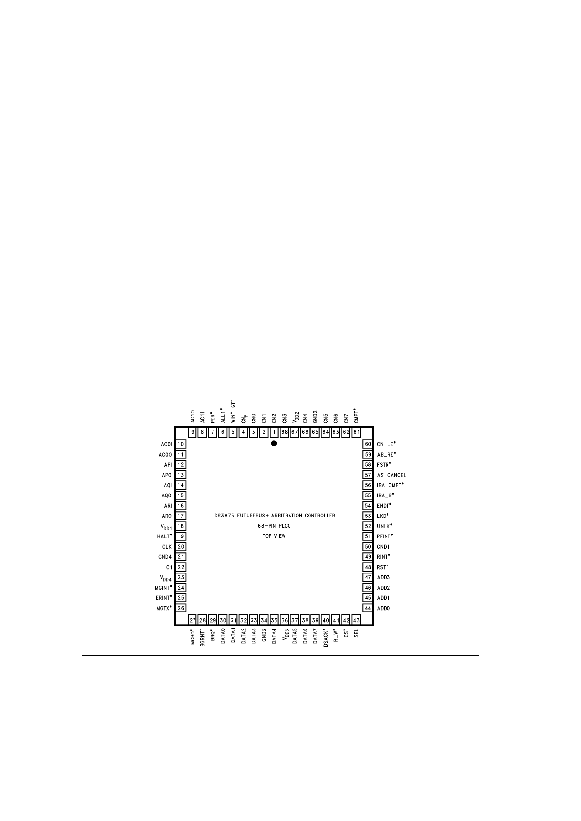
Table of Contents (Continued)
7.0 REGISTER DESCRIPTION (Continued)
7.6 CTRL2 ААААААААААААААААААААААААААААААААААААААААААААААААААААААААААААААААААААААААААААААААААААААААААААААААААА36
7.7 CTRL3 ААААААААААААААААААААААААААААААААААААААААААААААААААААААААААААААААААААААААААААААААААААААААААААААААААА36
7.8 STATE ААААААААААААААААААААААААААААААААААААААААААААААААААААААААААААААААААААААААААААААААААААААААААААААААААА37
7.9 STATUS ААААААААААААААААААААААААААААААААААААААААААААААААААААААААААААААААААААААААААААААААААААААААААААААААА37
7.10 RXCN0 ААААААААААААААААААААААААААААААААААААААААААААААААААААААААААААААААААААААААААААААААААААААААААААААААА37
7.11 RXCN1 ААААААААААААААААААААААААААААААААААААААААААААААААААААААААААААААААААААААААААААААААААААААААААААААААА38
7.12 RXMSG ААААААААААААААААААААААААААААААААААААААААААААААААААААААААААААААААААААААААААААААААААААААААААААААААА38
7.13 CLRERI ААААААААААААААААААААААААААААААААААААААААААААААААААААААААААААААААААААААААААААААААААААААААААААААААА38
7.14 CLRMGI АААААААААААААААААААААААААААААААААААААААААААААААААААААААААААААААААААААААААААААААААААААААААААААААА38
7.15 CLRPFI ААААААААААААААААААААААААААААААААААААААААААААААААААААААААААААААААААААААААААААААААААААААААААААААААА38
7.16 REV NO АААААААААААААААААААААААААААААААААААААААААААААААААААААААААААААААААААААААААААААААААААААААААААААААА39
8.0 PROGRAMMING REGISTERSАААААААААААААААААААААААААААААААААААААААААААААААААААААААААААААААААААААААААААААААА39
8.1 Host Write Cycle Using Falling Edge of DSACK*
(Figure T2a)
ААААААААААААААААААААААААААААААААААААААААААААААААААА39
8.2 Host Write Cycle Using Rising Edge of CS*
(Figure T2b)
АААААААААААААААААААААААААААААААААААААААААААААААААААААААА39
8.3 Host Read Cycle
(Figure T2c)
ААААААААААААААААААААААААААААААААААААААААААААААААААААААААААААААААААААААААААААААА39
9.0 CLOCK/TIMER/DELAY LINESААААААААААААААААААААААААААААААААААААААААААААААААААААААААААААААААААААААААААААААА39
10.0 RESET/INITIALIZATION/POWER UP ААААААААААААААААААААААААААААААААААААААААААААААААААААААААААААААААААААААА40
11.0 LIVE INSERTION АААААААААААААААААААААААААААААААААААААААААААААААААААААААААААААААААААААААААААААААААААААААААА41
12.0 LIVE WITHDRAWAL ААААААААААААААААААААААААААААААААААААААААААААААААААААААААААААААААААААААААААААААААААААААА42
13.0 TESTING THE DS3875 ААААААААААААААААААААААААААААААААААААААААААААААААААААААААААААААААААААААААААААААААААААА42
14.0 ELECTRICAL CHARACTERISTICS АААААААААААААААААААААААААААААААААААААААААААААААААААААААААААААААААААААААААА43
15.0 AC PARAMETERS ААААААААААААААААААААААААААААААААААААААААААААААААААААААААААААААААААААААААААААААААААААААААА43
TL/H/10747– 2
3

Pin Definition
Pin
Ý
of Pins Type Description
SIGNAL TO/FROM THE HANDSHAKE TRANSCEIVER
APO 1 O Arbitration handshake signal from the controller.
AQO 1 O Arbitration handshake signal from the controller.
ARO 1 O Arbitration handshake signal from the controller.
AC0O 1 O Arbitration condition signal from the controller.
AC1O 1 O Arbitration condition signal from the controller.
API 1 I Arbitration handshake signal from Futurebusa. This signal is the filtered and inverted version
of the Futurebus
a
backplane signal AP*.
AQI 1 I Arbitration handshake signal from Futurebusa. This signal is the filtered and inverted version
of the Futurebus
a
backplane signal AQ*.
ARI 1 I Arbitration handshake signal from Futurebusa. This signal is the filtered and inverted version
of the Futurebus
a
backplane signal AR*.
AC0I 1 I Arbitration condition signal from Futurebusa.
AC1I 1 I Arbitration condition signal from Futurebusa.
SIGNAL TO/FROM THE ARBITRATION TRANSCEIVER (Note: These pins are mapped to/from the DS3885 Futurebus
a
Arbitration Transceiver.)
CN(7:0) 8 I/O The bus to carry competition number to/from the arbitration transceiver.
CNp 1 O Parity bit of the competition number.
CMPT* 1 O Enables the Arbitration number onto Futurebusa.
ABÐRE* 1 O Direction control for the competition number bus to/from the transceiver.
CNÐLE* 1 O Latch enable for latching the Arbitration number from the controller into the transceiver.
PER* 1IPARITY ERROR: Indicates that a parity error was detected on the winner’s arbitration number.
WIN*ÐGT* 1 I Win signal when competing/greater than signal when not competing (used to preempt).
ALL1* 1 I Indicates that all the arbitration number lines on the bus are asserted (used for messages).
SIGNALS TO/FROM THE PARALLEL PROTOCOL CONTROLLER
BRQ* 1IBUS REQUEST: Indicates to the controller to acquire the bus for the module’s use.
BGRNT* 1OBUS GRANT: Signal asserted by the controller after the detection of a bus request. The
module can start using the bus.
RINT* 1 I Will put the arbitration controller in phase 0 and release all the bus lines except AR*.A
selective reset is performed. The rising edge will release controller from phase 0. This reset is
to be used for bus initialization.
RST* 1 I Reset signal from the host. An internal reset is performed. All bus signals are released. The
rising edge will put the controller in phase 0 (same as power-up reset).
HALT* 1 I Will halt the arbitration controller in phase 0. This signal is for use during live insertion.
ENDT* 1IEND OF TENURE: Indicates the true end of bus tenure of the current master. This line may be
asserted only after all the parallel protocol lines are released. (Generated via external logic
from BRQ* released.)
4
Pin Definition (Continued)
Pin
Ý
of Pins Type Description
SIGNALS TO/FROM THE HOST (CPU Plus External Interface Logic)
DATA(7:0) 8 I/O Data bus for the host to access the register bank of the controller.
ADD(3:0) 4 I Address bits for the register bank of the controller.
CS* 1ICHIP SELECT: The host can read or write to/from the controller.
RÐW* 1 I Read/write signal from the host.
DSACK* 1 O Data acknowledge pin for host read/write.
SEL 1 I SELECT: Determines how the controller latches in data. A ‘‘1’’ on the pin uses the rising
edge of CS*. A ‘‘0’’ on the pin uses the falling edge of DSACK*.
MGRQ* 1IMESSAGE REQUEST: Indicates to the controller to send an arbitration message.
MGTX* 1OMESSAGE TRANSMIT: Indicates the successful transmission of an arbitration message.
ERINT* 1OERROR INTERRUPT: Indicates that an error occurred during the arbitration cycle.
MGINT* 1OMESSAGE INTERRUPT: Indicates the reception of an arbitration message.
PFINT* 1OPOWER FAIL INTERRUPT: Indicates that a powerfail message was received.
EXTERNAL LOGIC
IBAÐCMPT* 1 O Signal to indicate that the Parallel Protocol controller may assert its bit on the ADDRESS/
DATA bus if it is participating in an Idle Bus Arbitration.
IBAÐS* 1 I This signal indicates that IBA was successful. If this module was a competitor in the IBA
competition (!BRQ*), then this module is the winner and now the bus master. If this module
was the master, but did not compete in the IBA competition and IBA was successful, then the
M bit (Status register) is negated.
ASÐCANCEL 1 I Indicates the start of the disconnection phase of the current master or cancel the current
arbitration cycle.
LKD* 1ILOCKED: Signal to indicate that resources have been locked in the current tenure and
hence generate either a dummy cycle if current master or UNLK* otherwise. (Decoded from
Futurebus
a
Command port output from Data Path Unit.)
UNLK* 1OUNLOCK: Transfer of tenure indication to the parallel protocol controller for unlocking its
resources. Generated only if the LKD* signal is asserted. (To external logic.)
FSTR* 1OFIFO STROBE: Signal generated to load an external FIFO for received arbitration messages.
CLK 1 I Clock input to the internal PLL.
C1 1 I External capacitor input for PLLÐ0.1 mF.
5

1.0 Introduction to Futurebus
a
Futurebusais a high-performance asynchronous multiplexed address/data backplane bus designed by the IEEE
896.1 committee for use in a wide variety of multiprocessor
architectures. The Futurebus
a
standard is a next generation backplane bus standard developed to a set of requirements including openness, performance, and system facilities and flexibilities so as not to hinder systems using this
bus for many generations of computer systems. Futurebus
a
is a single cache coherent backplane architecture
featuring scalability, technology independent protocols, and
explicit provisions to extend to future applications. Requirements set for the Futurebus
a
architecture by the IEEE
896.1 Futurebus
a
Working Group include:
1. Architecture, processor, and technology independent
2. A basic asynchronous (compelled) transfer protocol
3. An optional extended source-synchronized protocol
4. No technology-based upper limit to bus performance
5. Fully distributed parallel and arbitration protocols
6. Support for fault-tolerant and high-availability systems
7. Support for cache-based shared memory
8. Compatible message transport definition.
Compatibility of varying speed and technology boards connected to the same Futurebus
a
backplane is dependent
upon broadcast capability, or a snooping cache coherence
scheme. The performance of a Futurebus
a
backplane is
scalable over time to allow a low-end 32-bit system operating at 100 Mbytes/sec to be expanded to a 256-bit system
operating at 3.2 Gbytes/sec in the future. This performance
is attainable by the use of source-synchronized protocols
which eliminate spatial skews and receivers which are triggered by the incident wave from the driver. The synchronization protocol of the Futurebus
a
backplane allows the
synchronization domain of the sender to extend along the
backplane, presenting only one synchronization interface
between the bus and the receiver.
The Futurebus
a
backplane uses ‘‘Backplane Transceiver
Logic’’ (BTL). BTL is a signaling standard that has been
developed to enhance the performance of backplane buses. This standard eliminates the settling time delays, that
severely limit the TTL bus performance, to provide significantly higher bus transfer rates. BTL compatible transceivers feature low output capacitance drivers to minimize bus
loading, a 1V nominal signal swing for reduced power consumption, and receivers with precision thresholds for maximum noise immunity. For example, all Futurebus
a
signals
are open collector with termination resistors (selected to
match the bus impedance) connected to 2V at both ends.
The low voltage is typically 1V. All Futurebus
a
signals are
active low, indicated by an * after the signal name. (Refer to
Table I.) Further, signals can be driven simultaneously by
several modules. This requires that glitch filtering will be
needed for those times to filter out the transmission line
effect called the wire-or glitch. Refer to the Futurebus
a
specifications for details.
TABLE I. Signal Definitions
Signal Type,
Terminology
Logic
TTL BTL
Example Signal Level
Active High Asserted Logic 1 5V Ð
SignalÐName
Negated Logic 0 0V Ð
Active Low Asserted Logic 1 0V 1V
SignalÐName*
Negated Logic 0 5V Ð
Released
Logic 0 Ð 2V
(Open Collector)
2.0 Introduction to Futurebus
a
Arbitration
Futurebusauses an evolved version of the Parallel Contention Arbiter (see
Figure 4
). Through the application of a
unique arbitration vector to this logic, only one contender
will be uniquely selected as the winner. This implementation
requires no central logic on the backplane and gains the
following advantages:
1. The current master can see any requests and their priori-
ty to determine whether it should give up the bus.
2. Multiple priority levels can be implemented to allow sys-
tems to allocate bus bandwidth to modules running the
most critical tasks.
3. A Round Robin (fairness) protocol is implemented within
each priority level to ensure fair and equitable allocation
of bus tenure to all modules.
4. A master elect can be preempted by a higher-priority con-
tender. This allows the higher priority contender to access the bus with minimum latency (with some sacrifice
to the system performance).
5. Arbitration Messages or events can be broadcast on the
arbitration bus without disturbing the current transaction
on the parallel bus. Important system control functions
and interrupts can be sent using this mechanism without
the need of dedicated bus lines.
6. A Module may support either Idle Bus Arbitration or Park-
ing. Idle Bus Arbitration can be enabled by the current
master to decrease the arbitration latency when ony one
competitor is requesting the bus. If Idle Bus Arbitration is
not selected then Parking may be enabled by the master.
Parking allows the current master to regain bus tenure
(during Phase 0) to perform new bus transactions.
6
2.0 Introduction to Futurebus
a
Arbitration (Continued)
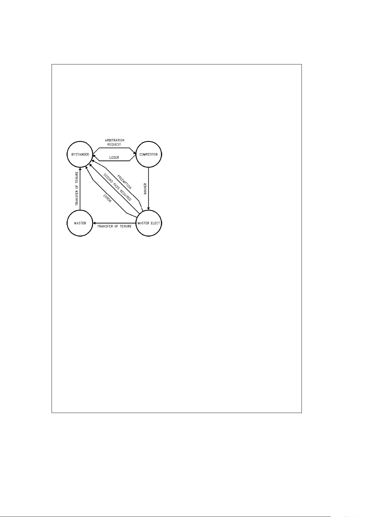
2.1 THE ARBITRATION STATES
Figure 1
is an Arbitration State Diagram showing four states
that a module may enter as well as the events that cause
the module to change states during the arbitration process.
Transitions from one state to another occur only when certain conditions are met, based on the arbitration phase and
the arbitration bus lines. Once a control acquisition cycle
has started, all modules must participate in the arbitration to
remain synchronized within the system.
TL/H/10747– 3
FIGURE 1
3.0 Introduction to DS3875
Arbitration Controller
The DS3875 Arbitration Controller implements the complete
requirements fo the IEEE 896.1 specifications. For example,
both arbitration modes of operation (Unrestricted and Restricted) are supported. Also, either Idle Bus Arbitration or
Parking may be selected for cases when only one request
or no request for bus competition exist. The controller is
software configurable to operate as a slow/fast module.
This selects the minimum time the arbitration controller
must wait during the arbitration competition before it can
read the resulting competition status. This delay allows arbitration competition lines (AB[7... 0]*, ABP*) to settle due
to several arbitration numbers being applied to them (Wireored bus lines). Further, a built-in PLL, which accepts a
clock signal from 2 MHz to 40 MHz, in steps of 1 MHz,
controls several programmable delay lines used for releasing ar* after issuing CMPT*/IBAÐCMPT* (PS(1:0)). This
delay compensates for the chip to chip skew to ensure sufficient time to drive the arbitration competition number onto
the arbitration competition lines during normal arbitration; or
to assert the AD/DATA lines during Idle Bus Arbitration before releasing ar*. Internally, the PLL also generates the 1
ms timer used during arbitration phase 2 and phase 4.
The Arbitration Controller supports Arbitration message
sending. A FIFO strobe, FSTR*, is provided to store more
than one arbitration message externally to prevent overrun.
Also a hardwired register contains the first word of the arbitration message (h
Ê
1ff). Additional registers which hold arbitration numbers, status information, controller configuration
information, and an arbitration message can be accessed
by the host through Read/Write operations. For outgoing
arbitration numbers, the on chip parity generator unloads
the host of the parity generation function. For incoming arbitration numbers, the DS3885 Arbitration Transceiver performs the parity check function and drives the PER* input
signal to the Controller. Separate interrupt pins for error occurrence, reception of an arbitration message, and reception of Powerfail message are available. These interrupts
are cleared by performing a dummy write cycle to these
registers.
3.1 DS3875 Futurebus
a
Arbitration Controller (Distrib-
uted) Configuration for IEEE 896.1 Compliance
The DS3875 Futurebus
a
Arbitration Controller implements
the complete requirements of the IEEE 896.1 specification.
On chip reset (RST*), the arbiter defaults to the 896.1 compliance configuration features.
The D53875 Distributed Arbiter was designed before the
896.1 specification was finalized. Thus, it contains additional
options that can he selected in proprietary bus applications
or 896.1 compatible bus applications. There are three features in total that can be chosen through register programming.
First an explanation of each feature will be given, so that if
an application can take advantage of the option, it can be
programmed. Then, the 896.1 compliance configuration is
given so the arbiter will operate in complete accordance
with the specification.
Arbitration Number: Unrestricted/Restricted Mode
In Distributed Arbitration, both priority and fairness protocols
are implemented. Applications requiring quick access to the
Futurebus
a
backplane can be assigned high priority to reduce bus latency times. Applications with the same (equal)
need of the backplane bus, a fairness protocol is guaranteed. Thus, distributed arbitration implements a fairness protocol for modules assigned the same priority classification.
The arbitration competition number encodes this information onto eight lines: AB[7:0]and arbitration number line:
ABP. The Arbitration competition number consists of three
fields: priority, round robin, and geographical address. Distributed Arbitration protocol allows from 1 to 256 priority levels. Systems not requiring more then two priority levels, a
single pass competition number will suffice, one bit for priority. Systems with greater then two priority levels implemented will need a two pass competition number, where eight
bits are allocated for priority representation. Now, the competition number exactly contains: 5 bits for geographical address (this guarantees uniqueness), 1 bit for round robin,
either 1 bit for priority (single pass), or 8 bits for priority (two
pass), and 1 bit to designate if the number is single pass or
two pass. (Refer to Table II on page 14.)
When the DS3875 was designed, two modes of operation
were defined: Unrestricted and Restricted. The Unrestricted
mode allowed one and two pass competition numbers to
coexist in a system. The Restricted mode allowed only one
pass competition numbers. Now, the 896.1 specification
7

3.0 Introduction to DS3875
Arbitration Controller
(Continued)
only describes one method of operation. This method completely corresponds to the Unrestricted mode. In the
DS3875, the R-U* bit in the CTRL2 register, configures the
operation mode of the arbiter. On reset, the arbiter is placed
in the unrestricted mode, in accordance to the 896.1 specification.
Arbitration Competition Settling Time
Distributed Arbitration uses contention logic to select the
winner of the competition cycle. The Arbitration competition
begins with all competing modules asserting the most significant bit AB[7], of the competition number onto the backplane lines. A bit wise comparison is performed where modules are allowed to assert the subsequent bits only as long
as that module’s competition number bits thus far asserted
are greater than or equal to the bits seen on the backplane
lines. Thus, all competing modules begin asserting their
competition numbers onto the backplane lines, but at the
end, only the winning module will be allowed to assert it’s
competition number onto the backplane lines.
When the DS3875 was designed, two speeds where allowed in the FBUS
a
backplane system for the arbitration
competition settling time: Slow or fast. During the arbitration
cycle, modules would indicate if they had a fast or slow
competition settling time. If any module indicated that it had
a slow competition settling time, then all modules would
compete using the slow competition settling time, else, the
fast settling time would be used during the competition cycle. The DS3875 allows the user to program a fast or a slow
competition settling time. One of eight settling times can be
selected for each mode with 16 total possible delay times.
The IEEE 896.1 specification now allows each module to
use it’s worst case arbitration settling time, t
A
, as the module’s delay time to determine it’s win/lose status for the
arbitration competition. The ones and zeros combination in
the competition number plays a significant role in determining the numbers settling time. Several factors are incorporated into the t
A
calculation:
tpd: Maximum end to end signal propagation delay along
the transmission line (backplane). This is a function
of the maximum length of the transmission line.
tint: Delay between a change on any arbitration line,
ABx*, on the
input to a module
and the correspond-
ing
change on that module’s adjacent
arbitration
output, ab[x-1]*,orabp*, as its competition number
is applied to or withdrawn from those bits.
text: Delay between a change on any arbitration line,
ABx*,onthe
input of any other competing module
and the corresponding
changes on that module’s
arbitration outputs, ab[x-1]*,orabp*, as its competi-
tion number is applied to or withdrawn from those
bits.
twin: Maximum delay between the time when the arbitra-
tion bus, AB[7..0]*, becomes stable and equivalent
to cn[7..0]on the input to a module and the indication within that module that it is the winner.
(Refer to 896.1 for more details).
Thus, now each module can evaluate it’s win/lose condition
when it’s t
A
time has elapsed. During a particular competition, the winning module’s competition number will have the
longest worst case settling time since this is the module that
has placed all of it’s competition number bits onto the
FBUS
a
.
To use the DS3875 in the 896.1 compliant mode, the user
programs two delay values in the CTRL2 register that are
closest to the calculated worst case settling time for the
particular competition number. The FÐS* bit should correspond to the table (fast or slow) that the most desired delay
resides. The CTRL2 register bits PD3 to PD5 program the
delay number that corresponds to the fast mode operation,
and PD0 to PD2 program the delay number that corresponds to the slow mode operation. Thus, a delay that is
closest to the desired delay time should be selected both
from the fast (PD3 to PD5) table and the slow (PD0 to PD2)
table. The FÐS* bit will configure this arbiter in the fast or
slow mode of operation.
8

3.0 Introduction to DS3875
Arbitration Controller
(Continued)
CTRL2
7 6 543210
F
Ð
S*R
Ð
U*PD5 PD4 PD3 PD2 PDl PD0
During the competition cycle, if any module has selected the
slow mode of operation, AC0* is asserted during phase 1
for indication to all modules to operate in the slow mode.
Thus, each arbitration cycle will determine whether the programmed fast delay value or the programmed slow delay
value is used for the arbitration number settling time delay.
The range of values in the fast and slow delay tables are
very close to each other and in some cases are exactly the
same that the desired delay value can be easily chosen.
The DS3875 is in complete accordance with 896.1 since
AC0* signal now only is evaluated in phase 3, 4, and 5, and
the t
A
number is individually determined for each number.
Idle Bus Arbitration
Previously, the Futurebus
a
specification allowed idle bus
arbitration. Idle Bus Arbitration (IBA) gives a module quick
access to Futurebus
a
when the current master has completed it’s transfers. IBA occurs on the parallel highway,
AD[31:0]lines. When the arbitration cycle is in phase 0 and
the master module is not carrying out transactions, another
module initiates normal arbitration and IBA simultaneously.
In IBA, each module is assigned a particular AD[31:0]bit to
assert if a module wishes to get tenure of the bus. If more
then one module asserts a bit onto the address/data lines
then normal arbitration on the arbitration bus lines will determine the new master. If only one module asserted a bit on
the address/data line, then during phase 2 of the normal
arbitration cycle that module will be given a bus grant signal.
Thus, IBA was specified to speed up the arbitration process
when there are not multiple contenders for the bus.
IEEE 896.1 no longer allows IBA. Now, only Parking is allowed. It lets the current Futurebus
a
master quickly access
the bus to perform other transfers when no other modules
want to use it. Parking issues the BGRNT* signal to the
current bus master during Phase 0.
For IEEE 896.1 compliance in the DS3875, the IBAÐPK* bit
of the CTRL3 register should disable IBA and enable Parking. On chip reset, Parking is selected. The IBAÐCMPT*
output signal of the DS3875 should not be connected and
IBAÐS* input signal should be connected to V
CC
.
Concluding Remarks
In retrospect, features which are no longer part of IEEE
896.1 specification were discussed. All of these features are
user selectable. The DS3875 can be easily configured to
operate in the 896.1 compliance mode. As a matter of fact,
on power up reset, the DS3875 is configured in the compliance mode. Briefly:
1. Arbitration Number:
CTRL2 register: RÐU* bit
Unrestricted mode now corresponds with
the 896.1 arbitration number representation scheme.
2. Arbitration Settling Time Delay:
CTRL2 register: Program as desired.
Select a delay from the fast table and
slow table that closely matches the worst
case arbitration settling time number, t
A
.
3. IBA:
CTRL3 register: IBAÐPK* bit
Enable Parking for 896.1 compliance
which simutanously disables IBA.
9
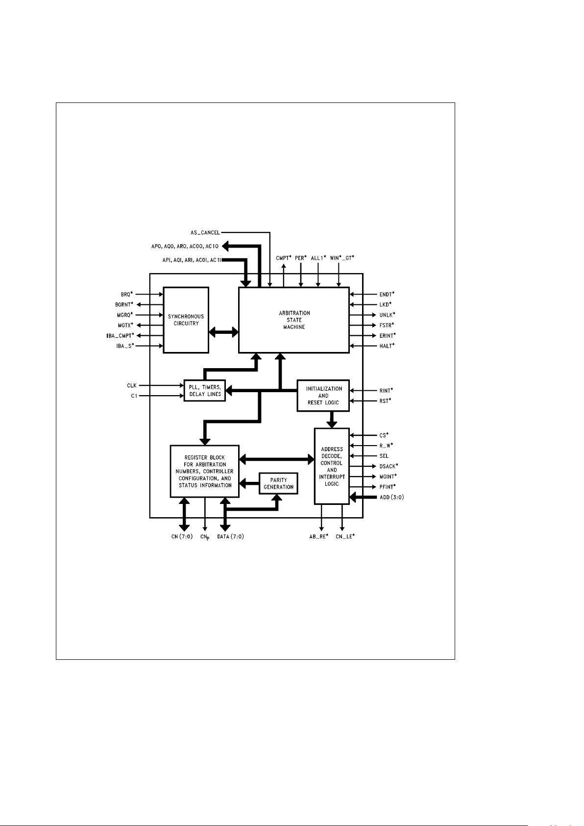
4.0 DS3875 Interfaces
The Arbitration Controller interfaces with the DS3884A
Handshake Transceiver, DS3885 Arbitration Transceiver,
host with other support chips, Protocol Controller, and Reset and Initialization logic.
Figure 2
depicts an internal block diagram of the DS3875
Arbitration Controller.
Figure 3
shows the interface between
the DS3875 Arbitration Controller and the other logic on the
module.
The DS3884A Handshake Transceiver drives the arbitration
handshake and condition signals to the arbitration controller
(API, AQI, ARI, AC0I, AC1I). The Arbitration Controller continuously monitors the Futurebus
a
backplane through
these signals. Whether the Arbitration Controller is competing in the current control acquisition cycle or not, it drives
the arbitration handshake and condition signals (APO, AQO,
ARO, AC0O, AC1O) which the handshake transceiver
drives onto the Futurebus
a
backplane.
TL/H/10747– 4
FIGURE 2
10
4.0 DS3875 Interfaces (Continued)
TL/H/10747– 5
FIGURE 3
When competing the DS3885 Arbitration Transceiver is enabled to place the competition numbers CN(7 . . . 0) and its
associated parity bit, CNp, onto the Futurebus
a
backplane.
During every cycle, whether or not competing, the winning
module’s arbitration number is read, the value of
WIN*ÐGT* signal and PER* signal is determined and updated in the appropriate internal registers.
The host can read or write (R/W) into the Arbitration Controller registers to change the controller configuration,
check status, or R/W a new arbitration number/message.
The host can select to latch data either on the falling edge
of DSACK* or on the rising edge of CS* by releasing or
asserting the SEL pin.
The Module may become bus master during Phase 5 if the
normal arbitration cycle was successful, Phase 0 if Parking
was successful, or Phase 2 if IBA was successful. Upon
becoming bus master, the Arbitration Controller will issue
BGRNT*. This signal indicates to the Protocol Controller
that it can now perform the desired transactions on the Parallel address/data bus.
The Protocol Controller will let the Arbitration Controller
know if it has locked resources by asserting the LKD* signal. If resources were locked, then at transfer of tenure, the
Arbitration Controller will issue UNLK* to the Protocol Controller to unlock resources.
A dummy cycle will be initiated by the Arbitration Controller
to perform the unlocking function if lock (LKD*) is still asserted after end of tenure (ENDT*) is asserted and no other
modules are competing. Unlock will be asserted at the
transfer of bus tenure (even if this module wins the competition). If another module initiates arbitration competition this
module will participate in the competition and will issue the
unlock (UNLK*) signal upon transfer of bus tenure. When
the bus transaction is complete and no resources are
locked, the Protocol Controller has the option of enabling
either Idle Bus Arbitration or parking (IBAÐPK* in CTRL3).
11

4.0 DS3875 Interfaces (Continued)
The input signal ALL1* (AB[7...0]*and ABp* all asserted)
is used to determine if any module is sending an arbitration
message during pass 1. For convenience, the Arbitration
Controller outputs FSTR* (to an external FIFO) during message reception so more than one arbitration message may
be stored by the module.
The Arbitration Controller has dedicated interrupt pins
(ERINT*, MGINT*, PFINT*) that interface with the Protocol
Controller so that important messages and error indications
can be quickly detected.
The Protocol Controller will issue the message request or
bus request signals to the DS3875. When a message has
been transmitted (Second Pass of arbitration, Phase 5), the
Arbitration Controller will assert MGTX*.
On board reset, initialization, power-up, and live insertion
logic will inform the Arbitration Controller which type of reset
operation to perform: Power-Up Reset (RST*), Initialization
(RINT*), or live insertion (HALT*). See Sections 10.0 and
11.0 for more information.
5.0 Arbitrating for Futurebus
a
The arbitration process allows a module to seek and gain
tenure of Futurebus
a
to transfer data to or from another
module. The arbitration process is independent of the data
transfer process and may take place concurrently with data
transactions on Futurebus
a
. If a module (or several modules) want to use the bus, an arbitration competition takes
place. The module with the highest arbitration number gets
tenure of the bus.
The National Semiconductor solution to Futurebus
a
arbitration includes the DS3875 Arbitration Controller, the
DS3885 Arbitration Transceiver and the DS3884 Handshake Transceiver (see front page system block diagram).
More information on Arbitration as it applies to the Futurebus
a
IEEE standard is available in Section 5 of the ‘‘Futu-
rebus
a
P896.1 Logical Layer Specification’’.
5.1 UNRESTRICTED/RESTRICTED MODES OF
OPERATION
The Arbitration Controller supports either the Unrestricted
or the Restricted mode of arbitration. In the system environment, all modules must be configured to operate in the
same mode at any given time.
During initialization, the Unrestricted mode is set since it
must be supported by all modules. The Unrestricted mode
allows a single pass of an 8-bit arbitration number or a two
pass of a 16-bit arbitration number to be used.
Futurebus
a
allows arbitration numbers requiring a single
pass control acquisition cycle to be mixed with those requir-
ing a two pass control acquisition cycle. During the first pass
of a two pass cycle, more than one module may have the
same number; however, during the second pass only one
winner results where the competition numbers must be
unique. A logic zero in the RUÐbit of the CTRL2 register
selects the unrestricted mode.
The Restricted mode of operation is optional and is selected
by setting the RUÐbit to a logic one in the CTRL2 register.
This mode limits arbitration numbers to 8 bits. Thus, only a
single control acquisition cycle occurs where all numbers
are unique. The arbitration numbers are assigned by the
module and can be dynamically changed.
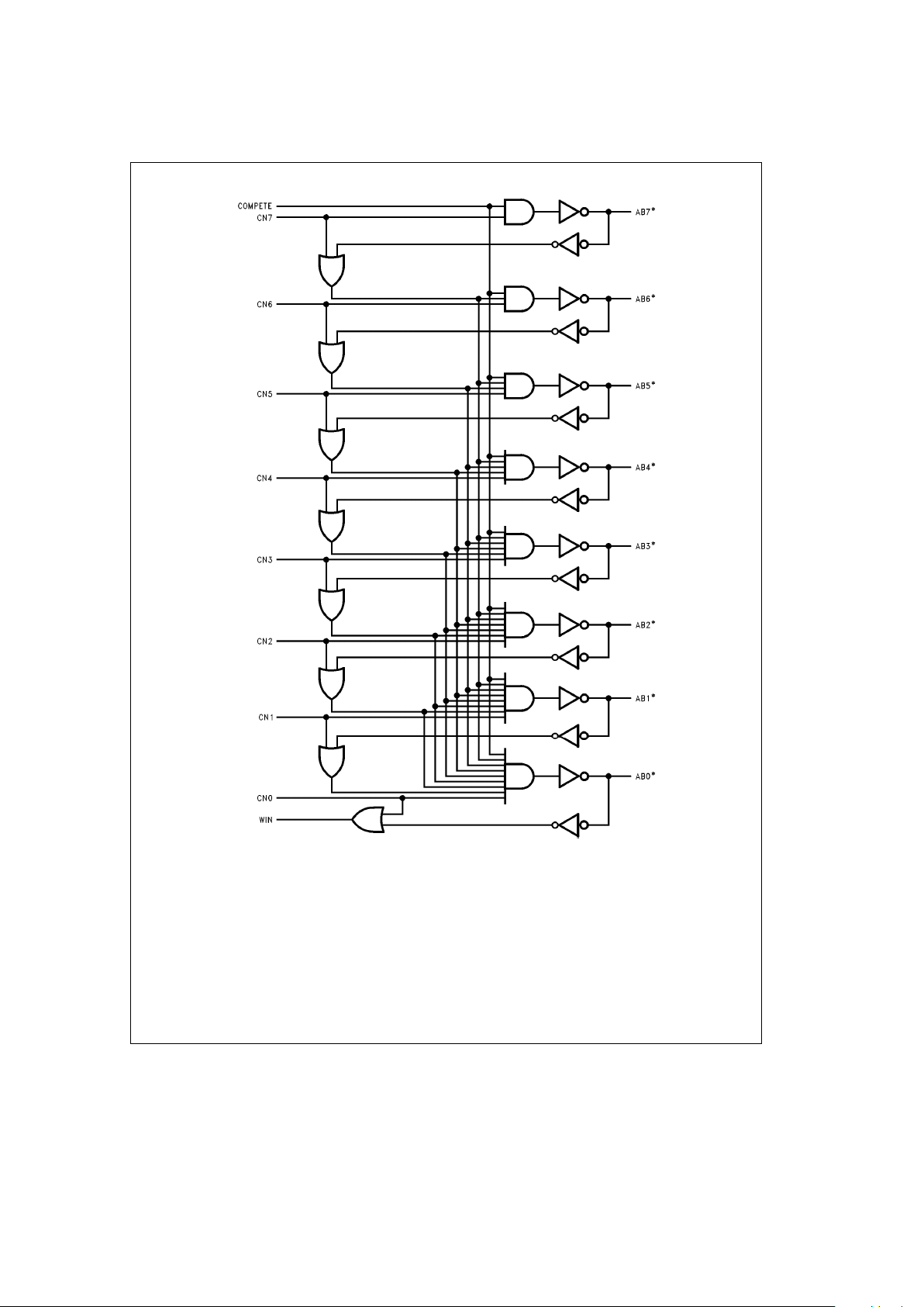
5.2 THE ARBITRATION NUMBER AND ARBITRATION
CIRCUIT
Each module has a unique arbitration number. When two or
more modules compete for the bus, the module with the
highest arbitration number will win the competition.
The DS3885 Arbitration Transceiver contains the arbitration
circuit. See
Figure 4
for a functional model of the arbitration
circuit. A Parallel Contention Arbitration Protocol controls
how modules assert and release the AB[7 ... 0]* and
ABp*. After a period of time (ta) the protocol ensures that
only the winners arbitration number will remain on the
AB[7... 0]*and ABp*.
The arbitration number consists of one or two competition
numbers, CN(7 . . . 0). The Arbitration Controller Transmits/
Receives the competition number to/from the Arbitration
Transceiver. The CNÐLE* signal latches the competition
number into the transceiver while the ABÐRE* signal allows the controller to read in the winner’s competition number. Along with the competition number, the Arbitration Controller transmits the CNp bit, the generated parity bit of the
competition number, to the Arbitration Transceiver. Odd
parity, as specified in the Futurebus
a
specifications, is implemented. Thus, CNp is set when even number of ones are
present in the competition number. When CN(7 . . . 0) is
received from the Arbitration Transceiver, the PER* bit is
checked for error detection.
Referring to Table II, in the Unrestricted mode, the CN7 bit
indicates if the module requires another arbitration pass.
When a one pass and a two pass arbitration number occur
in the same control acquisition cycle, the one pass arbitration number will win.
The DS3875 allows the module to dynamically change the
arbitration number by writing into the TXCN0 and/or the
TXCN1 registers (see Section 7). If the arbitration number is
changed during an arbitration cycle it will be used in the next
arbitration competition.
The arbitration number is composed of three fields: Priority
Field, Round Robin Field, and a Unique Field.
12
5.0 Arbitrating for Futurebus
a
(Continued)
TL/H/10747– 6
FIGURE 4. FuturebusaFunctional Model of the Arbitration Circuit
13
5.0 Arbitrating for Futurebus
a
(Continued)
5.2.1 Priority Field (PR)
The priority field represents a module’s priority class which
is determined by the system designer. In the unrestricted
mode, the length of this field is a maximum of eight bits
while in the restricted mode it is two bits.
5.2.2 Round Robin Field (RR)
This field is represented by a single bit, CN5, in both modes
of operation. The round robin protocol ensures that all modules in the same priority class have fair and equal access of
the bus. A module is allowed to get tenure of the bus in a
sequence defined by its value in the unique field.
The round robin bit is adjusted by the Arbitration Controller
each time a transfer of tenure occurs in the module’s same
priority class whether or not the module is competing in the
control acquisition cycle. In the module’s same priority
class, the round robin bit is set when tenure of the bus is
transferred to a module with a larger unique field value or
the round robin bit is cleared when tenure of the bus is
transferred to a module with a lesser unique field value.
In the event, where the module’s arbitration number is
changed, after the next control acquisition cycle, the round
robin bit is adjusted accordingly.
5.2.3 Unique Field (U)
The five bit unique field, CN(4 . . . 0), guarantees the uniqueness of the module’s arbitration number. The unique number may correspond to the module’s geographical address
or may be allocated by the system designer as he chooses
while also in such a way that minimizes the arbitration settling time. The value ‘‘11111’’ is not allowed in systems using arbitration messages.
5.3 ARBITRATION CATEGORIES
A module can be in one of six categories when a control
acquisition cycle is in progress;
#
Competitor for the Parallel bus
#
Competitor to send a message
#
By-Stander
#
By-Stander who decides to invoke Pre-emption
#
Master
#
Master Elect
5.3.1 Competitor for the Parallel Bus
A Module may become a competitor for the parallel bus if it
issues a Bus Request (! BRQ*) to the arbitration controller
before the arbitration cycle Phase 1 starts, see
Figure 5a
.
If the module issues a bus request and the arbitration cycle
is in phase 0, the controller will assert APO to start an arbitration competition. If an arbitration competition has already
started, and the module’s bus request comes prior to API
being asserted on the arbitration bus, the module may enter
this arbitration cycle. If an arbitration competition has already started, and the module’s bus request comes after
AP* being asserted on the arbitration bus, the module will
have to wait until the next arbitration cycle to compete (or
pre-empt the current arbitration cycle in Phase 3).
TABLE II. Arbitration Number
Bit CN7 CN6 CN5 CN4 CN3 CN2 CN1 CN0
Unrestricted ModeÐSingle Pass
Pass 1 1 PR0 RR U4 U3 U2 U1 U0
Unrestricted ModeÐTwo Pass
Pass 1 0 PR7 PR6 PR5 PR4 PR3 PR2 PR1
Pass 2 1 PR0 RR U4 U3 U2 U1 U0
Restricted Mode
Pass 1 PR1 PR0 RR U4 U3 U2 U1 U0
Arbitration Message
Pass 1 11111111
Pass 2 a7 a6 a5 a4 a3 a2 a1 a0
14

5.0 Arbitrating for Futurebus
a
(Continued)
5.3.2 Competitor to Send a Message
The Arbitration Controller supports message sending. Message sending is implemented in the unrestricted mode in a
two pass arbitration cycle. The first pass of all ones (1FF H)
in the competition number identifies the transaction as a
message. The ALL1* input signal is asserted by the Arbitration Transceiver when it detects 1FF H on the AB[7...0]*
and ABp* lines. The arbitration controller has a hardwired
register that holds the first pass word. Further, a dedicated
pin MGRQ* (message request) places the Arbitration Controller in the message sending mode.
The message that is to be transmitted is loaded into the
TXMSG register. The message of 1FF H is reserved as the
powerfail message. Other messages are to be coded by the
system designer with the greater priority messages having a
higher arbitration number. Obviously, if more than one module simultaneously desires to send a message, the message
with the highest arbitration number will be transmitted.
When a message is sent, no transfer of tenure takes place.
Thus, the master (M) or the round robin (RR) bits are not
updated. Upon successfully transmitting the message,
MGTX** signal is asserted.
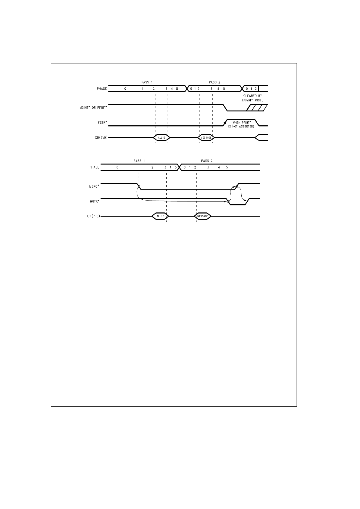
When a message is received by the Arbitration Controller
(Phase 5), message interrupt (MGINT*) is asserted and
FIFO Strobe (FSTR*) is negated. In the case of a Powerfail
message being received; the PFINT* signal is asserted.
When the PFINT* signal is asserted, the MGINT* and
FSTR* signals are not generated. See
Figure 5d
.
When sending a message, once the MGRQ* signal is asserted, until the message has been transmitted, all other
requests are blocked. Upon the MGTX* signal being released, the message request signal will be reevaluated to
see if another message needs to be sent.
If this module is the module sending the arbitration message, then the message interrupt (MGINT*) or the Powerfail
interrupt (PFINT*) will not be generated on this module.
These interrupts are generated only upon the reception of a
message from another module. Refer to
Figure 5e
.
5.3.2.1 Using an External FIFO to Store Messages
The Arbitration Controller provides a FIFO strobe (FSTR*)
signal to store more than one arbitration message in an
external FIFO. A rising edge on FSTR* is generated upon
the reception of an arbitration message.
See
Figure 3
and Timing Diagrams: T6, Phase 2 and Phase
5.
1. FSTR* is always asserted (! FSTR*) during phase 2.
2. FSTR* is negated (FSTR*) during phase 5 given the following conditions.
1. The message is not being sent by this module.
2. This is the second pass of an arbitration message.
3. No errors occurred during this arbitration cycle.
4. This is not a powerfail interrupt message (! PFINT*).
The external latch shown in
Figure 3
is enabled by ABÐRE*
to temporarily hold the message. While ABÐRE* is low
(see timing diagrams phase 2 and 5), the latch is fall
through. Then, during phase 5 on the rising edge of FSTR*,
the message held in the latch will be strobed into the FIFO.
5.3.3 By-Stander
A Module is considered a by-stander in the arbitration competition if it does not issue a Bus Request (! BRQ*)tothe
arbitration controller before arbitration cycle Phase 1 starts.
5.3.4 By-Stander Who Decides to Invoke Pre-emption
A module with a higher arbitration number than the master
elect may initiate a new arbitration cycle to establish a new
master. This process, referred to as pre-emption, allows a
high priority to acquire tenure of the bus with minimum latency.
Pre-emption is allowed in phase 3 when all of the following
conditions are met:
1. the arbitration number is greater than the arbitration
number on the bus
2. a bus request signal was recently received
3. did not participate in the arbitration competition phase 2.
The master elect may be preempted by asserting AC1O.
Pre-emption is not allowed during:
#
the first pass of a two pass cycle
#
message sending
These two events are given higher precedence.
If a module decides to preempt and changes its competition
number during phase 2 or phase 3 in the Arbitration Controller, the Arbitration Transceiver will still use the current
latched competition number to make the greater than comparison. When the next arbitration cycle occurs, the new
competition number will be used.
5.3.5 Master
The Master is the module that currently has tenure of the
parallel bus.
5.3.6 Master Elect
The Master Elect is the module that won the current arbitration cycle. The Master Elect will become master upon transfer of tenure.
15
5.0 Arbitrating for Futurebus
a
(Continued)
TL/H/10747– 7
a. Normal Bus Request Timing
TL/H/10747– 8
b. Idle Bus Arbitration Timing
TL/H/10747– 9
c. Parking
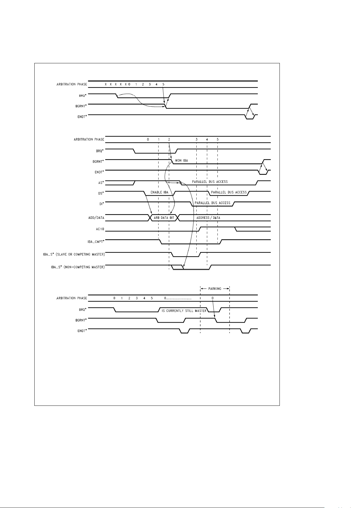
FIGURE 5. Bus Request Timing (Normal Arbitration, Idle Bus Arbitration and Parking)
16
5.0 Arbitrating for Futurebus
a
(Continued)
TL/H/10747– 10
d. Message Receiving
TL/H/10747– 11
e. Message Sending
FIGURE 5. Bus Request Timing (Normal Arbitration, Idle Bus Arbitration and Parking) (Continued)
5.4 FUTUREBUS
a
OPTIONAL MEANS OF
ARBITRATION
Besides the normal Futurebus
a
Parallel Contention Arbitra-
tion, the Futurebus
a
Specification allows two other option-
al arbitration methods to acquire the parallel bus quickly:
#
Idle Bus Arbitration
#
Parking
Both of these arbitration methods are supported by the National Semiconductor DS3875 Arbitration Controller.
5.4.1 Idle Bus Arbitration (IBA)
Idle Bus Arbitration (IBA) is selected by setting the IBAPK*
bit in CTRL3 register. The aim of IBA is to give a module
quick access to Futurebus
a
when the current master has
completed its transfers.
IBA is invoked the same as a normal arbitration bus request
(! BRQ*) but uses the parallel bus (AS* negated, DS* asserted, and the parallel address/data bus) to determine the
winner of the arbitration cycle, see
Figure 5a, b
.
During normal arbitration the transfer of Futurebusatenure
occurs during phase 5. During IBA the transfer of Futurebus
a
tenure occurs during phase 2. During IBA the AC1O
arbitration condition signal will be asserted by the new master. This will cancel the transfer of tenure during the normal
arbitration cycle. Note that Futurebus
a
tenure was transferred but only the two modules involved in the IBA (the
master and the master elect) know that the transfer of ten-
ure has taken place. All the other modules involved in the
normal arbitration cycle see that the transfer of tenure during the normal arbitration cycle was canceled.
If two or more modules have a request, then normal arbitration will determine which module will gain access. IBA takes
place on the parallel highway, AD/DATA (31 . . . 0). Each
module is assigned a bit which is to be asserted during IBA.
If only one bit is asserted during the IBA competition, then
IBA issues the bus grant signal to that module. Concurrently
with IBA, normal arbitration takes place. If a module does
not want IBA to issue a bus grant, IBA may be inhibited by
asserting DI*. During phase 5, normal arbitration will determine appropriate actions.
5.4.1.1 Masters Support Circuitry to Enable IBA
If IBA is allowed, it is invoked during phase 0. In order to
support IBA external logic is needed in addition to the arbitration controller. The Masters external logic must monitor
the arbitration control acquisition synchronization signals
(AP*,AQ*,AR*) and the parallel bus address handshake
signals (AS*,AK*,AI*). If the master supports IBA it should
wait until it is ready to end its bus tenure (ENDT* asserted).
Then when it releases AS* it should assert ds* to enable
modules to participate in IBA competition.
5.4.1.2 Modules Support Circuitry to Participate in IBA
If a module wants to use IBA to gain tenure of Futurebus
a
it must use external logic to monitor the arbitration control
17

5.0 Arbitrating for Futurebus
a
(Continued)
acquisition synchronization signals (AP*,AQ*,AR*), the
parallel bus address handshake signals (AS*,AK*,AI*), the
parallel bus data sync signal (DS*) and data acknowledge
inverse (DI*), and the IBAÐCPT* output from the arbitration
controller.
5.4.2 Parking
During Power Up, the Arbitration Controller is programmed
to perform either Idle Bus Arbitration or Parking by setting or
clearing the IBAPK* bit in the CTLR3 register. Parking is
selected by clearing the IBAPK* bit. The aim of Parking is to
give the Futurebus
a
bus Master quick access to the bus to
perform other transfers when no one else desires to use it.
Thus, it is not necessary for the master to go through the
entire arbitration cycle to get the BGNT* signal. Parking issues BGNT* in Phase 0, see
Figure 5c
. If another module
gets a message request or bus request, the arbitration competition cycle begins like it normally does to handle the request.
All of the following conditions should be met to take advantage of Parking:
1. Parking in selected
2. module must be the current Master
3. ENDT* signal is high
4. BGRNT* signal is high
5. BRQ* signal is asserted low while in phase 0
6. LKD* signal is high (Resources are not locked)
When these conditions are true, the Arbitration Controller
issues the BGRNT* signal (asserted low) in phase 0. Upon
end of tenure, BGRNT* signal will be released. The Master
may continue to use Parking to perform transactions until
after the arbitration competition cycle selects a new master
(see
Figures 5c
and7).
Parking is allowed only when the Master has all resources
unlocked (indicated by LKD* signal being high). During
phase 0, if the master still has resources locked (ENDT*
and BGRNT* signals are high), the Arbitration Controller will
immediately initiate a dummy cycle to unlock resources. The
UNLK* signal is generated during phase 5 upon the successful transfer of tenure. The transfer of tenure may be
with itself or another module.
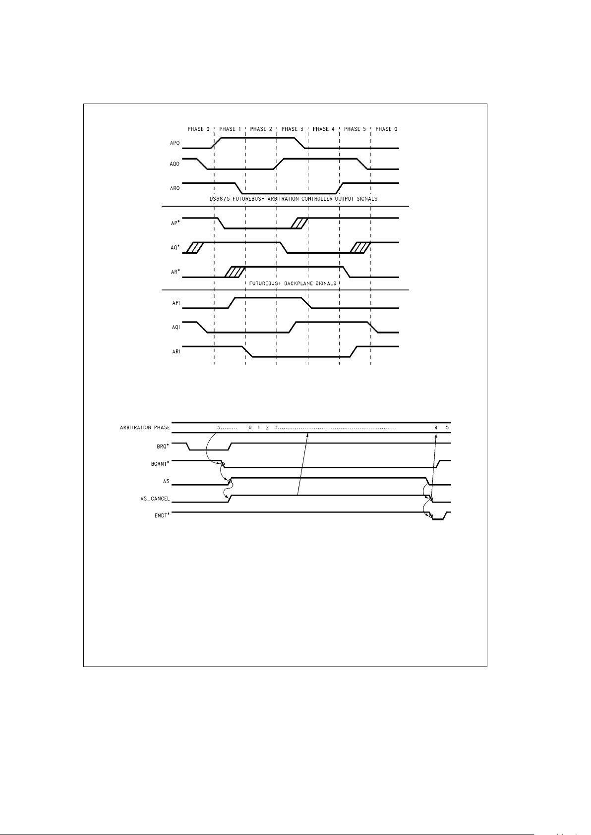
5.5 THE ARBITRATION PHASES
The arbitration process consists of transitioning through six
phases (Phase 0 thru Phase 5) of the three arbitration synchronization signals (AP*,AQ*,AR*). To transition between
control acquisition phases only one of the three arbitration
synchronization signals will transition.
The Arbitration process is asynchronous and occurs as fast
as all the modules that contain arbitration logic can transition through the arbitration phases. If a two-pass arbitration competition has been selected the entire control acquisition cycle is repeated twice.
Each arbitration synchronization signal (AP*,AQ*,AR*)
represents the wire-OR of each of the individual synchronization signals from each of the modules. For any of the
synchronization signals on the bus to be released, all the
modules must release their individual synchronization signals (ap*,aq*,ar*). Therefore, the release of a synchroniza-
tion signal forms a global synchronization point for all the
modules. Likewise, during the assertion of a synchronization
signal all modules must remain synchronized by asserting
their own signals in response.
Each module must participate in the control acquisition cycle, whether or not the module is competing, to remain synchronized with the other modules.
Figure 6
is a timing dia-
gram of the Control Acquisition Sequence.
Figures 7a –f
are
state transition diagrams of the DS3875 Arbitration Controller. Tables III and IV represent the internal register bits that
are affected by the arbitration states and their transitions.
The DS3875 Arbitration Controller transitions to the next
arbitration phase upon (see
Figure 6
):
1. APO output signal being asserted to phase 1
2. ARI input signal being negated to phase 2. (This input is
filtered and indicates all modules have released the AR*
synchronization signal on the Futurebus
a
backplane.)
3. AQO output signal being asserted to phase 3
4. API input signal being negated to phase 4. (This input is
filtered and indicates all modules have released the AP*
synchronization signal on the Futurebus
a
backplane.)
5. ARO output signal being asserted to phase 5
6. AQI input signal being negated to phase 0. (This input is
filtered and indicates all modules have released the AQ*
synchronization signal on the Futurebus
a
backplane.)
18
5.0 Arbitrating for Futurebus
a
(Continued)
TL/H/10747– 12
DS3875 FUTUREBUSaArbitration Controller Input Signals
FIGURE 6a. Arbitration Phases
B. Single Access, ASÐCANCEL Timing Diagram (AS is tied directly to the
ASÐCANCEL Input of the Arbitration Controller)
TL/H/10747– 13
FIGURE 6b. Timing of the ASÐCANCEL Signal
19

5.0 Arbitrating for Futurebus
a
(Continued)
C. Multiple Accesses, ASÐCANCEL Timing Diagram (AS is latched before being input to the ASÐCANCEL
input of the Arbitration Controller. At the end of the last transfer the latch is reset)
TL/H/10747– 14
D. Multiple Accesses, ASÐCANCEL Timig Diagram (AS is tied directly to the ASÐCANCEL input
of the Arbitration Controller. The Master must guarantee that the second transfer, or ENDT*, will come within
1 ms of the falling edge of the initial transfer AS signal).
TL/H/10747– 15
FIGURES 6c, 6d. Timing of the ASÐCANCEL Signal
5.5.1 Phase 0, Idle Phase
This Phase is characterized by AP* released and AR* asserted on Futurebus
a
and AQf negated on the module
board. See
Figure 7a
for the DS3875 Arbitration Controller
Phase 0 state diagram.
The arbitration controller will be negating APO, asserting
ARO and be receiving AQI negated. This is the state of the
arbitration synchronization lines when no control acquisition
cycle is in progress or between the two control acquisition
cycles of a two-pass arbitration sequence.
While in Phase 0 the following actions are performed:
1. If ! HALT* is asserted the arbitration controller will not
transition to Phase 1 until HALT* is negated.
2. If any of the ‘‘New Bits’’ are set (NCN, NGO, NDS) the
corresponding internal arbitration controller registers will
be updated and then the ‘‘New Bits’’ will be reset.
3. The arbitration condition lines (AC1*, AC0*) will be negated.
One of the following three types of arbitration may occur
during Phase 0:
1. Normal arbitration
2. Idle Bus Arbitration (IBA)
3. Parking
5.5.1.1 Phase 0, Normal Arbitration Events That Cause a
Transition to Phase 1
There are five conditions during normal arbitration where
APO will be asserted causing a transition to Phase 1:
1. If Two-Pass Arbitration is selected, a bus request has
been received (! BRQ*
a
! MGRQ*aDummy Cycle)
and this module was a winner during the first pass of
arbitration, then APO will be asserted.
2. Though this module may not be requesting Futurebus
a
another module may want to arbitrate for Futurebus
a
and assert AP*. This action will cause the AP input (API)
on this module to be asserted. API asserted will cause
this modules arbitration controller to assert APO.
3. If this module is currently the master and ! LK* is asserted, BGRNT* is negated, ! ENDT* has been received, no
other requests have been received and API is negated,
the module will initiate a dummy cycle to unlock its resources by asserting APO (if it is doing Single Pass or the
First Pass of Two-Pass Arbitration).
4. A message request (! MGRQ*) will cause APO to be asserted (if it is doing Single Pass or the First Pass of TwoPass Arbitration). Note that if both a bus request
( ! BRQ*) and ! MGRQ* are received during phase 0,
20

5.0 Arbitrating for Futurebus
a
(Continued)
! MGRQ* will be given a higher priority and will be acted
upon during this arbitration cycle. ! BRQ* will wait to arbitrate during the next arbitration cycle.
5. A Bus Request (! BRQ*) will cause APO to be asserted
(if it is doing Single Pass or the First Pass of Two-Pass
Arbitration). This will cause the Futurebus
a
AP* to be
asserted and will indicate to the other modules that an
arbitration competition is beginning.
Note that the user will violate the Futurebus
a
specification
if he leaves the local modules resources locked (! LKD*)
and has IBA enabled in the arbitration controller. This incident is dangerous because it could lead to another module
winning IBA with the local modules resources being locked.
If the other module tried to access the local modules resources it would result in deadlock.
5.5.1.2 Phase 0, Idle Bus Arbitration Events That Cause
a Transition to Phase 1
If IBA is desired and the arbitration cycle is in Phase 0
(! APO, ! AQI, ARO), the parallel bus is idle (AS*,AK*,!AI*),
and DS* has been released for a minimum period of time
(Futurebus
a
spec.) the Masters external logic may assert !
DS*. This will alert any module capable of doing IBA that
IBA has been enabled.
5.5.1.3 Phase 0, Parking
The aim of Parking is to give the Futurebus
a
bus master
quick access to the bus to perform other transfers when no
one else desires to use it. If Parking is enabled (! IBAÐPK*)
and is successful the arbitration controller will issue BGNT*
in Phase 0. If another module gets a message request or
bus request, the arbitration competition cycle begins like it
normally does to handle the request (see Section 5.5.4 for
more information).
5.5.2 Phase 1, Decision Phase
This Phase is characterized by AP* and AR* asserted and
AQ* released on Futurebus
a
. See
Figure 7b
for the
DS3875 Arbitration Controller Phase 1 state diagram.
The arbitration controller will be asserting APO and ARO
and negating AQO. This is the state of the arbitration synchronization lines when the decision phase (1) is in progress.
During Phase 1 the individual modules must make the decision whether they want to compete. This decision will be
based upon the state of the modules bus request, message
request or locked status (! BRQ* or ! MSGRQ* or ! LKD*)at
the time APO is asserted. Since this condition is subject to
mestastability a metastable hardened latch is used internal
to the DS3875 to resolve this potential condition.
If the module is going to compete the arbitration competition
number (CN(7:0)) and its parity bit (CNp) will be asserted to
the arbitration transceiver, Latch enable of the arbitration
transceiver will be asserted and negated (! CNÐLE* asserted for 20 ns) to latch in the arbitration number, and compete
will be asserted (! CMPT*) to enable the arbitration competition number onto Futurebus
a
.
If the module is a slow module (! FS*, see Section 7.6) the
arbitration handshake signal AC0O will be asserted.
Once the decision to compete has been made, the arbitration handshake signal (! AC1O) that cancels the arbitration
cycle will be negated. The Programmable Skew (PS(1:0))
gives time for the arbitration number to become valid on
Futurebus
a
before ARO is negated. Once the Programma-
ble Skew has timed out ARO will be negated. Once all modules have negated AR* the arbitration cycle will transition to
Phase 2.
Once all modules have negated AR* a1ms timer is started.
This timer is used to guarantee that the competition cycle
does not get stuck in phase 2. During Phase 2, the winner of
the competition cycle, after waiting its t
A
(arbitration settling
time) time, transitions the cycle to Phase 3. The timer is
used to prevent livelock where the winning module may not
transition the cycle to Phase 3.
5.5.2.1 Phase 1, Idle Bus Arbitration Events That Cause
a Transition to Phase 2
During phase 1 the arbitration controller will output ! IBA
Ð
CPT*. When the external logic sees ! IBAÐCTP* and the
parallel bus is inactive (AS*,AK*,!AI*) it should drive one
of the data bits of the parallel address/data bus.
5.5.3 Phase 2, Competition Phase
This Phase is characterized by AP* asserted and AQ* and
AR* released on Futurebus
a
. See
Figure 7c
for the
DS3875 Arbitration Controller Phase 2 state diagram.
The arbitration controller will be asserting APO, negating
AQO and receiving ARI negated. This is the state of the
arbitration synchronization lines when the competition
phase (2) is in progress.
While in Phase 2 the following actions are performed:
1. ABÐRE* is asserted after 30 ns. This allows the arbitra-
tion controller to monitor the winning competition number.
2. The FIFO STRobe is now asserted (! FSTR*).
There are two conditions that can cause AQO to be asserted causing a transition to Phase 3:
1. The AQI input being asserted.
2. Competing, arbitration competition settling time (t
a
) expired, one ms Phase 2 arbitration error timer not expired,
and the WIN*ÐGT* input being asserted.
5.5.3.1 Phase 2, Idle Bus Arbitration Events That Cause
a Transition to Phase 3
The external logic should drive the IBA Success signal
(! IBAÐS*) during phase 2 if DI* is released, only this modules data bit is driven on the data bus, and the arbitration
settling Time (t
s
) has not expired.
When the arbitration controller sees ! IBAÐS* asserted it
will issue bus grant (! BGRNT*) to give access of the bus to
the module that won the IBA. If two or more modules have a
request, then normal arbitration will determine which module will gain access.
5.5.4 Phase 3, Error Check Phase
This Phase is characterized by AP* and AQ* asserted AR*
released on Futurebus
a
. See
Figure 7d
for the DS3875
Arbitration Controller Phase 3 state diagram. Also see
Fig-
ures 6b, c, d
for how ASÐCANCEL relates to Phase 3.
The arbitration controller will be asserting APO and AQO,
and negating ARO. This is the state of the arbitration synchronization lines when the error check phase (3) is in progress.
While in Phase 3 the following actions are performed:
1. If the module is a competitor and winner of the arbitration, the W(winner) bit in the STATUS register is set.
2. Upon entering phase 3, after 20 ns, ABÐRE* is negated.
21

5.0 Arbitrating for Futurebus
a
(Continued)
There are seven conditions that will cause the arbitration
controller to negate APO:
1. This module has had a Bus ReQuest (! BRQ*), won IBA,
and asserted AC1O and AS.
2. The current master releases AS (! ASÐCANCEL). The
master has completed its transactions on the parallel
bus, see
Figures 6b, c, d
.
3. This module detected the 1 ms timeout or a parity error
occurred during the arbitration cycle. This error condition
will cause the assertion of AC0O and AC1O and ERINT*
signals which will inhibit the transfer of tenure during this
arbitration cycle.
4. Another module has detected that transfer of tenure is to
be inhibited (AC1I).
5. This module was competing and won the competition
where this is the first pass of a two pass arbitration cycle.
6. This module did not compete (CMPT*) but now has a
bus request (! BRQ*) and its competition number is
greater than (! WIN*ÐGT*) the modules competition
number that won the current arbitration competition. This
module preempts the current arbitration competition by
asserting AC1O. This inhibits the transfer of tenure during this arbitration cycle and allows a new arbitration cycle to be initiated in which this module can compete.
7. This module was competing (! CMPT*) and won the competition (W bit of Status register set) but the bus request
or message request has been negated (BRQ* or
MGRQ*). This error condition will cause the assertion of
AC0O, AC1O and ERINT* signals which will inhibit the
transfer of tenure during this arbitration cycle.
After all the modules have negated AP*, upon receiving
!API, the arbitration cycle will transition to Phase 4.
5.5.4.1 Phase 3, Idle Bus Arbitration Events That Cause
a Transition to Phase 4
During phase 3 of the arbitration cycle, when the current
master has not yet released the bus (AS), the new master (a
module that was competing (!IBAÐCMPT*) and won
(!IBAÐS*)) will drive AC1O to inhibit the transfer of tenure
during the normal bus arbitration cycle (tenure was transferred during the IBA cycle).
Note: The new master will now continue the normal arbitration process to
completion but may begin conducting transactions on the bus.
5.5.5 Phase 4, Master Release Phase
This Phase is characterized by AP* released, AQ* asserted,
and AR* released on Futurebus
a
. See
Figure 7e
for the
DS3875 Arbitration Controller Phase 4 state diagram and
Figures 6b, c, d
for how ASÐCANCEL relates to phase 4.
The arbitration controller will be receiving API negated, asserting AQO and negating ARO. This is the state of the
arbitration synchronization lines when the master release
phase (4) is in progress.
While in Phase 4 the following actions are performed:
1. All modules, other then the bus master, start a 1 ms timer. This is referred to as the Master release timer. The
master has 1 ms to complete its transactions or to inhibit
the transfer of tenure and proceed to phase 5. This timer
is specified in the Futurebus
a
specification so in the
event where the current master does not respond, the
master elect may assume mastership during phase 5.
2. The CMPT* signal is negated (CMPT*).
There are six conditions that can cause ARO to be asserted
causing a transition to Phase 5:
1. Transfer of tenure is inhibited indicated by the assertion
of AC1I.
2. Was not Master and the ARI input was asserted.
3. Was Master and did not cancel (! ASÐCANCEL) the arbitration competition, see
Figures 6b, c, d
.
4. There is no current master (immediately following power
up) so the master elect may assert ARO.
5. Was Master and did cancel (! ASÐCANCEL) the arbitration competition, see
Figure 6d
. In this case the current
master will assert AC1O to inhibit the transfer of tenure
during this arbitration cycle.
6. All modules other then the current master detect the
Master Release Timeout.
5.5.6 Phase 5, Tenure Transfer Phase
This Phase is characterized by AP* released, AQ* asserted,
and AR* asserted on Futurebus
a
. See
Figure 7f
for the
DS3875 Arbitration Controller Phase 5 state diagram.
The arbitration controller will be negating API and asserting
AQO and ARO. This is the state of the arbitration synchronization lines when the tenure transfer phase (5) is in progress.
While in Phase 5 the following actions are performed:
1. If IBAÐCMPT* signal was asserted, it is now negated
(IBAÐCMPT*).
2. The unlock signal (! UNLK*) will be asserted if locked
(! LKD*) is asserted and the arbitration condition signals
(AC0I, AC1I) are negated.
3. This phase will update the following status bits:
1. The Master status bit (bit 5) in the status register.
2. The Competitor status bit (bit 4) in the status register.
3. The WIN status bit (bit 3) in the status register.
4. The Uniqueness, round robin and priority fields of the
RXCN1 register.
5. The Priority field of the RXCN0 register.
There are four conditions that can cause AQO to be negated:
1. Had a message request (! MGRQ*) and won the competition (! WIN*ÐGT*). In this case the message transmitted output will also be asserted (! MSGTX*).
2. Competed for the bus (! CMPT*), there were no errors
(! AC0I, ! AC1I), and won the competition (! WIN*ÐGT*).
In this case the bus grant output will be asserted
(! BGRNT*) and the internal master bit will be set (M, bit
5 in the status register).
3. There were no errors (! AC0I, ! AC1I) and the module is
not the winner. Resets the M bit in the status register.
4. A Message was received. In this case either message
interrupt will be asserted (! MGINT*) or the powerfail interrupt (! PFINT*) will be asserted.
22

5.0 Arbitrating for Futurebus
a
(Continued)
When a message is received the FIFO strobe (FSTR*) will
be negated, strobing a new message into the external FIFO,
given the following conditions:
1. The message is not being sent by this module.
2. This is the second pass of an arbitration message.
3. No errors occurred during this arbitration cycle.
4. This is not a powerfail interrupt message (! PFINT*).
Once all the modules have negated AQ*, upon receiving
!AQI, the arbitration cycle will transition to Phase 0.
TL/H/10747– 16
FIGURE 7a. DS3875 Phase 0 Arbitration State Diagram
Note: **HALT* is assumed to be negated in this state diagram. Also, the arbitration Controller GO bit in CTRL3 register must be asserted for the controller to
accept requests. Otherwise this module may not compete but will be a by-stander.
Note 1: Idle Bus Arbritation during Phase 0 is not an internal state of the Arbitration Controller. It is shown in this state diagram only to give a better understanding
of Phase 0 arbitration.
Note 2: The Arbitration Controller does not check for LKD*, but it should not be asserted during IBA to be in compliance with the Futurebus
a
specification. If lock
was asserted during IBA another module could win IBA and try to access this modules locked resources, this would result in deadlock. Also, the Arbitration
controller does not check AS* &!DS*&DI*, this is left up to external logic and this must be the first pass if two pass arbitration has been selected.
Note 3: The output ! di* from this module is driven from external control logic, it is only shown in this diagram to allow a clearer understanding of how IBA relates to
normal arbitration.
Note 4: Note that message request (MGRQ*) has a higher priority inside the arbitration controller then does bus request (BRQ*).
Note 5: This is a dummy arbitration cycle initiated to unlock (UNLK*) the modules resources. The dummy cycle is initiated, by the current master, if the modules
resources are still locked (! LKD*) after end of tenure (ENDT*) has been issued (*BGRNT* & Master&!LKD*& ENDT*) and the arbitration bus is idle.
Note 6: If this is the second pass of a two-pass arbitration cycle and a new request (! BRQ* or ! MGRQ*) is generated, that request will not be allowed to compete
until the next arbitration cycle. Note that pre-emption is allowed.
Note 7: If Two-Pass arbitration has been selected, Parking is only possible during Phase 0 of the first pass.
23

5.0 Arbitrating for Futurebus
a
(Continued)
TL/H/10747– 17
FIGURE 7b. Phase 1 Arbitration State Diagram
Note 1: Idle Bus Arbitration during Phase 1 is not an internal state of the Arbitration Controller. It is shown in this state diagram only to give a better understanding
of Phase 1 arbitration.
Note 2: One bit on the parallel data bus is driven by external logic (the arbitration controller only drives the ! IBAÐCMPT output) only if IBA is supported by the
module. Note that the arbitration controller does not require AS* &!DS*&DI*, external logic will require these conditions (from the Futurebus
a
specification).
Note 3: If a module does not want IBA to select a new master external logic around the arbitration controller will drive ! di*. This transition is shown in this diagram
to allow a clearer understanding of how IBA relates to normal arbitration.
Note 4: Competing
e
‘‘! BRQ*a! MGRQ*aDummy Cycle’’, WeW bit of STATUS register.
Note 5: These Requests must have occurred before APO was asserted or they will not compete until the next arbitration cycle.
Note 6: The possible metastable condition of ‘‘(! BRQ*
a
! MGRQ*aDummy Cycle) occurring at the same time as API’’ must be resolved before driving ! ARO.
Note 7: All conditions shown above the Phase 1 state must be completed before driving ! ARO.
24

5.0 Arbitrating for Futurebus
a
(Continued)
TL/H/10747– 18
FIGURE 7c. Phase 2 Arbitration State Diagram
Note 1: Idle Bus Arbitration during Phase 2 is not an internal state of the Arbitration Controller. It is shown in this state diagram only to give a better understanding
of Phase 2 arbitration.
Note 2: Bus Grant (! BGRNT*) is driven by the arbitration controller during Phase 2 only if IBA was successful for this module and the Arbitration settling time (ta)
has not expired. Also, DI* is shown here to indicate that IBA is allowed to select a new Master. DI* is not an Arbitration Controller signal. DI* is represented here for
completeness shake only to give a better understanding. Also, external logic will release the bit on the Parallel data bus.
Note 3: This transition to Phase 3 occurs when this module was competing, its arbitration settling time expired, and the one micro-second Phase 2 error timer has
not expired.
25

5.0 Arbitrating for Futurebus
a
(Continued)
TL/H/10747– 19
FIGURE 7d. Phase 3 Arbitration State Diagram
Note 1: Idle Bus Arbitration during Phase 3 is not an internal state of the Arbitration Controller. It is shown in this state diagram only to give a better understanding
of Phase 3 arbitration.
Note 2: AC1O is asserted to cancel the transfer of bus tenure if IBA was successful.
Note 3: AS is asserted if IBA was successful for this module.
Note 4: A Module will pre-empt another module if it did not compete in the present competition yet its arbitration number is higher than the current winner. In this
instance the pre-emption module will assert AC1O to cancel the transfer of tenure and allow a new competition to take place. Preemption is not allowed in the 1st
pass when the arbitration cycle consists of two pass.
Note 5: If a module that competed and won no longer is issuing a bus or message request, AC1O will be driven to cancel the transfer of tenure and ! ERINT* will be
driven to indicate an error has occurred.
Note 6: AC1O (if IBA was successful) and the W STATUS bit (if competing and won) must be asserted before driving ! APO.
Note 7: Competing
e
! BRQ*a! MGRQ*aDummy Cycle.
Note 8: All actions in this phase are performed after the arbitration number is latched.
26

5.0 Arbitrating for Futurebus
a
(Continued)
TL/H/10747– 20
FIGURE 7e. Phase 4 Arbitration State Diagram
Note 1: The Arbitration controller releases its arbitration number on Futurebusaby negating CMPT* to the arbitration transceiver.
Note 2: If no master or master error occurred, on timeout, assert ARO so the master elect may take over the bus.
Note 3: NoÐMaster
e
No Current Master of Futurebusaduring Powerup or Initialization.
27
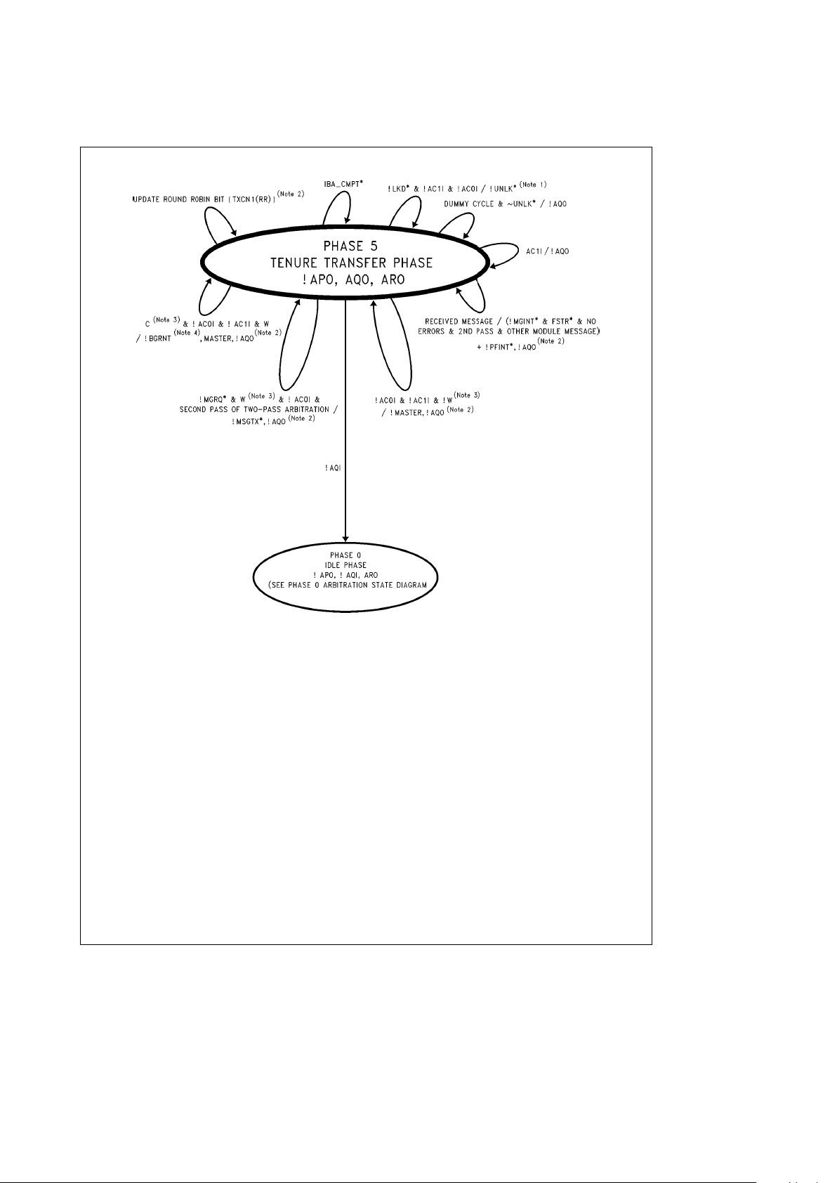
5.0 Arbitrating for Futurebus
a
(Continued)
TL/H/10747– 21
FIGURE 7f. Phase 5 Arbitration State Diagram
Note 1: Unlock this modules resources if its resources were locked and this is restricted mode, one pass arbitration, or the second pass of a two-pass arbitration
cycle.
Note 2: Only update Master status bit, TXCN1 (RR), ! MGINT*, FSTR*, ! PFINT*, ! BGRNT*, or ! MSGTX* given that this is restricted mode, one pass arbitration, or
the second pass of a two-pass arbitration cycle.
Note 3: W
e
W bit in the STATUS register, CeC bit in the STATUS register.
Note 4: ! BRGNT* is not issued if this is a dummy arbitration cycle, initiated by the arbitration controller to unlock resources.
28

Arbitration Controller Internal Register Bit Changes
TABLE III. Restricted Mode Arbitration or Unrestricted Mode Arbitration
(One Pass, or Second Pass of Two Pass)
Modules Category
during Arbitration
TXCN1
RR
(Note 1)
All Bits
STATE
STATUS
RXCN0
All Bits
RXCN1
RXMSG
A(0:7) Reset, Set
CLRERI
Reset, Set
CLRMGI
CLRPFI
(Note 2)
W C M U(0:4) RR PO P1
Competitor 5 X 1, 2 0, 1 5 3 3 3 3 3 X, 4 X, 5
By-Stander 5 X 1 0 5 3 3 3 3 3 X, 4 X, 5
Sending Message X 1, 2 0, 1 3 X, 4 X, 5
Receiving Message X 1 0, 1 3 X, 4 X, 5
Pre-Emption X 3 3 3 3
IBA 5
X
5
3 3 3 3 3 X, 4 X, 5
(Note 4) (Note 5)
Parking
(Note 3)
Note: The number shown within the box defines the arbitration phase where the particular bit may change state.
Note 1: Note that the STATE Register is updated in each Phase of Arbitration.
Note 2: This is the new Masters Competition Number.
Note 3: Parking is only a Phase 0 event.
Note 4: The RR bit is only updated on the New Master.
Note 5: The M bit is updated if IBA succeeded during Restricted Mode, or Unrestricted Mode (One Pass or the First Pass of Two Pass Arbitration).
‘‘X’’ means that any Phase can update this bit (or bits).
‘‘,’’ is used in the table to depict the condition where a particular Status bit is Reset and where it is Set (Ex. 0, 1 means that this Status bit is Reset in Phase 0 and
Set in Phase 1).
‘‘– ’’ is used in the table to depict the condition where a particular Status bit may change within several sequential phases (Ex. 2– 4 means that this Status bit can
change in Phases 2, 3, or 4).
TABLE IV. Unrestricted Mode, First Pass of Two Pass Arbitration
Modules Category
during Arbitration
TXCN1
RR
(Note 1)
All Bits
State
Status
(Note 2)
RXCN0
All Bits
RXCN1
RXMSG
A(0:7) Reset, Set
CLRERI
Reset, Set
CLRMGI
CLRPFI
W C M U(0:4) RR PO P1
Competitor X 1, 2 0, 1 3 X, 4 X, 5
By-Stander X 1 0 3 X, 4 X, 5
Sending Message X 1, 2 0, 1 X, 4 X, 5
Receiving Message X 1 0, 1 X, 4 X, 5
Pre-emption X 3
IBA X 5 3 X, 4 X, 5
Parking (Note 3)
Note: The Number shown within the box defines the arbitration phase where the particular bit may change state.
Note 1: Note that the STATE Register is updated in each Phase of Arbitration.
Note 2: This is the new Masters Competition Number.
Note 3: Parking is only a Phase 0 event.
Note: ‘‘X’’ means that any Phase can update this bit (or bits).
Note: ‘‘,’’ is used in the table to depict the condition where a particular Status bit is Reset and where it is Set (Ex. 0, 1 means that this Status bit is Reset in Phase 0
and Set in Phase 1).
Note: ‘‘-‘‘ is used in the table to depict the condition where a particular Status bit may change within several sequential phases (Ex. 2-4 means that this Status bit
can change in Phases 2, 3, or 4).
29

TABLE V. Pre-emption
Category Pre-emption Case Result
Messages message vs message no pre-emption
message vs anything else pre-empt: no number
comparison
anything vs message no pre-emption
Restricted Mode restricted vs restricted pre-empt if:
TXCN1lRXCN1
restricted vs message no pre-emption
Unrestricted Mode 1 pass vs 2 pass pre-empt: no number
comparison
1 pass vs 1 pass pre-empt if:
TXCN1
l
RXCN1
2 pass vs 2 pass pre-empt if:
TXCN0
l
RXCN0
and
TXCN1
l
RXCN1
Note: All pre-emptions take place in the second pass of arbitration or the only pass of arbitration.
TL/H/10747– 29
FIGURE 12a. IBAÐRestricted or Unrestricted Single Pass
30

TL/H/10747– 30
FIGURE 12b. IBAÐUnrestricted Two Pass
6.0 The DS3875 Arbitration Controller Support
of Locking and Unlocking
The DS3875 Arbitration Controller supports locking and unlocking of the modules resources whether it is a master or a
slave (see
Figure 8
).
If the Module becomes master and wishes to lock the
slave’s resources, it should assert LKD* (! LKD*) after receiving bus grant (! BGRNT* from the arbitration controller),
and drive the appropriate lock command during the parallel
bus connection phase. This lock command (during the connection phase of the parallel bus) will cause the selected
slave module(s) to assert lock (! LKD*) to their arbitration
controller. Once the module has finished its parallel bus
transactions it will assert end of tenure (! ENDT*).
If the Master is in, or enters, Phase 0:
1. with end of tenure issued,
2. no other module has started an arbitration competition,
3. LKD* is still asserted,
4. a new bus request (! BRQ*) has not been issued
it will start a dummy arbitration competition cycle to unlock
all resources on the bus that were locked. The dummy cycle
will proceed through the normal arbitration competition except that no bus grant will be asserted if the module wins
the arbitration competition.
If another module has initiated an arbitration competition the
master will participate in the competition and no dummy cycle will be initiated.
During Phase 5, upon successful completion of the arbitration cycle unlock will be asserted (! UNLK*) until the lock
input is negated.
31

A. Master Module Lock and Unlock Timing Diagram
TL/H/10747– 22
B. Slave Module Lock and Unlock Timing Diagram
TL/H/10747– 23
FIGURE 8. Master and Slave Lock and Unlock Timing Diagrams
32

7.0 Register Description
TOTAL MEMORY MAP
ADDRESSABLE REGISTERS
0000 TXCN0 (R/W)
70
0001 TXCN1 (R/W)
70
0010 TXMSG (R/W)
70
0011 CTRL1 (R/W)
70
0100 CTRL2 (R/W)
70
0101 CTRL3 (R/W)
70
0110 STATE (R)
70
0111 STATUS (R)
70
1000 RXCN0 (R/W)
70
1001 RXCN1 (R/W)
70
1010 RXMSG (R/W)
70
1011 CLRERI (R/W)
70
1100 CLRMGI (R/W)
70
1101 CLRPFI (R/W)
70
1110
Reserved
1111 REV NO. (R)
70
HARDWIRED REGISTER
ALL 1s
80
Legend:
Register Type
Register RegisterÐName (Read/Write)
Address
ADD(3:0) MSB LSB
33

7.0 Register Description (Continued)
This section describes the addressable registers and the ALL1s hardwired register.
7.1 ALL1S
This register carries the first word of an arbitration message (h
Ê
1ff).
7.2 TXCN0 (ADD(3:0)
e
0000)
For the Unrestricted Mode, this register stores the pass 1 arbitration number of a two pass arbitration. (CN7e0). Defaults to
h
Ê
00.
76543210
0P7P6P5P4P3P2P1
Bit Symbol Description
0–6 P(1:7) Priority field of the arbitration number.
7 0 This bit is fixed at zero as specified in the Futurebus
a
specification for the pass 1 number of a
two pass arbitration.
Note: The Parity bit CNp for the arbitration number is internally generated during the time the host writes the numbers into the controller. The odd parity as
specified in the Futurebus
a
specifications is generated. CNp is set to one when even number of ones are present in the arbitration number.
7.3 TXCN1 (ADD(3:0)e0001)
For the Unrestricted Mode, this register stores the pass 2 arbitration number of a two pass arbitration, or stores the single pass
arbitration number (CN7
e
1). This register also stores the arbitration number used in the Restricted Mode. Defaults to hÊ80.
7 6 543210
1/P1 P0 RR U4 U3 U2 U1 U0
Bit Symbol Description
0–4 U(0:4) Uniqueness field of the arbitration number.
5 RR Round Robin bit of the arbitration number. Note: This bit is updated during phase 5, upon the
successful transfer of tenure. See Table III.
6 P0 Priority field of the arbitration number. If configured as a two pass arbitor, P0 is part of P(0:7). If
configured as a single pass arbitor, P0 is the priority field. If configured to arbitrate in restricted
mode then P0 is part of P(0:1).
7 1/P1 This bit is fixed at one as specified in the spec for the pass 2 number of a two pass arbitration,
and for the single pass arbitration number. This bit is P1 for the restricted mode arbitration
number.
Note: The Parity bit CNp for the arbitration number is internally generated during the time the host writes the numbers into the controller. The odd parity as
specified in the Futurebus
a
specifications is generated. CNp is set to one when even number of ones are present in the arbitration number.
34

7.0 Register Description (Continued)
7.4 TXMSG (ADD(3:0)
e
0010)
This register holds the arbitration message to be transmitted. Defaults to hÊff (Powerfail).
76543210
A7 A6 A5 A4 A3 A2 A1 A0
Bit Symbol Description
0–7 A(0:7) Arbitration message to be sent.
Note: The Parity bit CNp for the arbitration number is internally generated during the time the host writes the numbers into the controller. The odd parity as
specified in the Futurebus
a
specifications is generated. CNp is set to one when even number of ones are present in the arbitration number.
7.5 CTRL1 (ADD(3:0)e0011)
Control register 1. PS(1:0) programs the delay needed to ensure the assertion of the most significant 1 in CN(7:0) after compete
is issued before the release of ar*, or, during IBA, this delay ensures there is sufficient time to assert the AD/DATA lines before
the release of ar*. PC(5:0) programs the internal divider to receive a clock input from 2 MHz to 40 MHz in steps of 1 Mz. During
chip reset, (RST*) the divider is set to receive a clock of 20 MHz. This input clock divider should be programmed during
initialization for the desired frequency. Defaults to h
Ê
14.
76543210
PS1 PS0 PC5 PC4 PC3 PC2 PC1 PC0
Bit Symbol Description
0–5 PC0 –PC5 Programs the internal input clock divider to receive a clock from 2 MHz to 40 MHz, in steps of
1 MHz.
The binary value of the clock frequency is coded with PC5 being the MSB. For example, to
program the divider to receive a 25 MHz signal PC5:PC0 bits are: 011001. To program the
divider to receive a 10 MHz signal PC5:PC0 bits are: 001010.
6–7 PS0 –PS1 Programs the chip to chip skew when releasing AR* in phase 1.
PS0 PS1 DELAY
00 0ns
01 5ns
1 0 15 ns
1 1 25 ns
This delay ensures that after compete is issued to the transceiver sufficient time is allowed for
the number to be put on the bus before releasing AR*. It also provides a means to provide
sufficient time for asserting AD/DATA lines during IBA before the release of ar*.
35

7.0 Register Description (Continued)
7.6 CTRL2 (ADD(3:0)
e
0100)
Control register 2. This register stores two parameters FSÐ(Fast/Slow) and DSÐ(Restricted/Unrestricted) that configure the
controller to operate in the chosen mode. PD(5:3) selects one of eight delays for the fast module and PD(2:0) selects one of
eight delays for the slow module. Defaults to h
Ê
00.
7 6 543210
F
Ð
S*R
Ð
U*PD5 PD4 PD3 PD2 PD1 PD0
Bit Symbol Description
0–5 PD0 –PD5 Programs the arbitration delay that is timed in a competition. These bits give a total of
16 selectable delays, 8 fast and 8 slow. PD0–PD2 select the slow module’s delay and
PD3–PD5 select the fast module’s delay.
(PD5 PD4 PD3) Fast (PD2 PD1 PD0) Slow
000 100 000 125
001 120 001 165
010 145 010 210
011 165 011 255
100 190 100 300
101 210 101 345
110 235 110 385
111 255 111 430
6R
Ð
U*R
Ð
U*Restricted/Unrestricted:
0 Configures the controller to arbitrate in unrestricted mode.
1 Configures the controller to arbitrate in restricted mode.
7F
Ð
S*F
Ð
S*Fast/Slow:
0 Configures the controller as a slow module.
1 Configures the controller as a fast module.
7.7 CTRL3 (ADD(3:0)e0101)
Defaults to hÊ00.
76 5 43210
TCSEL IBAÐPK* NCN NDÐS* NGO DÐS* G0
Bit Symbol Description
0 GO GO Bit:
1 indicates that all the required initialization is complete and the controller may accept
requests.
0 the controller will follow the normal flow of arbitration along with other modules
(bystander).
1D
Ð
S* D
Ð
S*Double/Single
0 Configures the controller to arbitrate in a single pass arbitration mode.
1 Configures the controller to arbitrate in a two pass arbitration mode.
2 NGO A ‘‘one’’ indicates that a new GO bit has been loaded. This bit is reset automatically when the new
GO bit takes effect. To be set by the user when the GO bit is changed.
3ND
Ð
S*A ‘‘one’’ indicates that a new DÐS* bit has been loaded. This bit is reset automatically when the new
DÐS* bit takes effect. To be set by the user when the DÐS* bit is changed.
4 NCN A ‘‘one’’ indicates that a new CN has been loaded. This bit is reset automatically when the new CN
takes effect. This bit is set internally when TXCN1 is accessed while the GO bit is set.
5 IBAÐPK* Idle Bus Arbitration/Parking:
1 Configures the controller to do Idle Bus Arbitration.
0 Configures the controller to do Parking.
6 TCSEL A ‘‘one’’ indicates that a test clock is being fed through the CLK pin to test the timers and counters in
the controller.
36

7.0 Register Description (Continued)
7.8 STATE (ADD(3:0)
e
0110)
This register contains the present state of the arbitration controller. This information may be used for testing and debugging
purposes. Defaults to h
Ê
01.
76543210
ST5 ST4 ST3 ST2 ST1 ST0
Bit Symbol Description
0–5 ST(0:5) These bits indicate the current phase of the arbitration controller.
7.9 STATUS (ADD(3:0)e0111)
This register contains status information and internal counter/divider test bits. The M, C, W bits default to zero. The counter test
bits may be evaluated when feeding in a test clock.
76543210
M C W CT2 CT1 CT0
Bit Symbol Description
2–4 CT(0:2) Counter test bits:
CT2Ðset to one when 1 ms timeout occurs.
CT1Ðset to one when divide by 40 divider has divided 40 times.
CT0Ðset to one when divide by n divider has divided n times.
5 W Win attribute of the module. A ‘‘one’’ indicates that the module is the winner of the current
arbitration cycle/pass.
6 C Competitor attribute of the module. A ‘‘one’’ indicates that the module is competing for the bus.
7 M Master attribute of the module. A ‘‘one’’ indicates that the module is the current master of the
bus.
7.10 RXCN0 (ADD(3:0)e1000)
This register stores the received pass 1 arbitration number of a two pass number (CNe0). Defaults to hÊ00.
76543210
0P7P6P5P4P3P2P1
Bit Symbol Description
0–6 P(1:7) Priority field of the current master/master elect arbitration number. This register is used only if
the controller is configured to arbitrate in Unrestricted two pass mode.
7 0 This field is fixed at zero as specified in the Futurebus
a
spec for the pass 1 number of a two
pass arbitration.
37

7.0 Register Description (Continued)
7.11 RXCN1 (ADD(3:0)
e
1001)
This register stores the received pass 2 arbitration number of a two pass arbitration number, or the single pass arbitration
number, (CN7
e
1) in the Unrestricted mode. Also this register stores the Restricted Mode arbitration number. Defaults to hÊ80.
7 6 543210
1/P1 P0 RR U4 U3 U2 U1 U0
Bit Symbol Description
0–4 U(0:4) Uniqueness field of the current master/master elect.
5 RR Round Robin bit of the current master/master elect.
6 P0 Priority field of the current master/master elect. If configured as a two pass arbitor, P0 is part of
P(0:7). If configured as a single pass arbitor, P0 is the priority field. If configured to arbitrate in
restricted mode then P0 is part of P(0:1).
7 1/P1 This field is fixed at one as specified in the spec for the pass 2 number of a two pass arbitration,
and for the single pass arbitration number. This bit is P1 for the restricted mode arbitration
number of the current master/master elect.
7.12 RXMSG (ADD(3:0)e1010)
This register stores the received non-powerfail arbitration message. Defaults to hÊ00.
76543210
A7 A6 A5 A4 A3 A2 A1 A0
Bit Symbol Description
0–7 A(0:7) Non-powerfail arbitration message received from another module.
7.13 CLRERI (ADD(3:0)e1011)
Error bits to indicate Parity, no BRQ/MGRQ or a timeout error. A dummy write into this register clears the error interrupt and all
the error bits. Defaults to h
Ê
00.
76543210
ER3 ER2 ER1
Bit Symbol Description
7 ER3 Error bit 3: indicates to the winner of the arbitration cycle that BRQ/MGRQ signal is no longer
present.
6 ER2 Error bit 2: indicates a timeout error.
5 ER1 Error bit 1: indicates a Parity error.
7.14 CLRMGI (ADD(3:0)e1100)
7.15 CLRPFI (ADD(3:0)
e
1101)
A dummy write into these registers clears the respective interrupt.
76543210
Bit Symbol Description
0–7
38

7.0 Register Description (Continued)
7.16 REV NO. (ADD(3:0)
e
1111)
Revision number of the controller.
76543210
R7 R6 R5 R4 R3 R2 R1 R0
Bit Symbol Description
0–7 R(0:7) REV NO.
8.0 Programming Registers
During power up, the registers should be initially programmed. The host may read/write to/from the register
block at any time. The host may select to write data into the
register either on the falling edge of DSACK* or on the rising edge of CS*. A zero on the SEL input pin configures the
controller to latch in data on the falling edge of DSACK*
while a one sets the controller to latch in data on the rising
edge of CS*. Refer to the timing diagrams (see
Figures T2a,
b, c
).
8.1 HOST WRITE CYCLE USING FALLING EDGE OF
DSACK*
(Figure T2A)
1. RÐW* signal is negated.
ADD(3:0) contains the address of the register to be accessed. (Note: The setup time with respect to CS* must
be satisfied.)
2. CS* is asserted (! CS*).
3. When the proper setup time of CS* to the rising edge of
clock is met and CS* is low for at least 3 clock cycles,
then DATA(7:0) will be latched into the register, by the
falling edge of DSACK*, on the 3rd rising clock edge
after the assertion of CS*. If the CS* setup time is not
met and CS* is low for at least 3 clock cycles, then
DSACK* is asserted and the data (DATA(7:0)) is latched
into the arbitration register on the following 3rd or 4th
rising clock edge after the assertion of CS*.IfCS*is
negated (CS*) before 3 clock cycles, then DSACK* is
not generated and as a default, DATA (7:0) is latched
into the arbitration controller register on the rising edge
of CS*.
4. Host negates CS*.
5. Arbitration Controller negates DSACK* (DSACK*)ifit
was asserted.
8.2 HOST WRITE CYCLE USING RISING EDGE OF CS*
(Figure T2b)
1. RÐW* signal is negated.
ADD(3:0) contains the address of the register to be accessed. (Note: The setup time with respect to CS* must
be satisfied.)
2. CS* is asserted (! CS*).
3. DSACK* is asserted (! DSACK*) by the Arbitration Controller when CS* is asserted for at least three clock cycles. If CS* is negated (CS*) before three clock cycles,
DSACK* is not asserted. The DSACK* signal may be
used or ignored by the system designer, in this case.
4. Host negates CS*. DATA (7:0) which satisfied the setup
time to the rising edge of CS* is latched into the arbitration controller register.
5. Arbitration Controller negates DSACK* (DSACK*)ifit
was asserted.
8.3 HOST READ CYCLE
(Figure T2c)
1. RÐW* signal is set high.
ADD (3:0) contains the address of the register to be accessed. (Note: The setup time with respect to CS* must
be satisfied.)
2. CS* is asserted (! CS*).
3. The data will be available on the DATA (7:0) bus within
the access time specified in the AC timing section.
4. The Data Strobe ACKnowledge (DSACK*) signal is generated as an acknowledge to the host signifying the validity of the accessed data. DSACK* may be used to insert WAIT states to the host during a host read cycle.
When the proper setup time of CS* to the rising edge of
clock is met and CS* is low for at least three clock cycles, DSACK* is asserted (! DSACK*) on the 3rd rising
clock edge after the assertion of CS*. If the CS* setup
time was not met and CS* is low for at least three clock
cycles, then DSACK* is asserted on the following 3rd or
4th rising clock edge after the assertion of CS*.IfCS*is
not low for at least 3 clock cycles, DSACK* is not generated.
5. Host reads data and negates CS* (CS*).
6. Arbitration Controller negates DSACK* (DSACK*)ifit
was asserted.
9.0 Clock/Timer/Delay Lines
(See
Figure 9
.) The input clock signal (CLK) to the arbitration controller is assumed to be a clock from 2 MHz to 40
MHz, in steps of 1 MHz.
The clock signal is also used for synchronization purposes
during read or write transfers. This is accomplished by synchronizing the DSACK* (Data Strobe Acknowledge) output
from the Arbitration Controller to the clock during arbitration
controller register reads or writes.
The binary value of the input clock (CLK) frequency is loaded into the CTRL1[5:0]register. This value is used to program the divide by n counter to scale the input clock down
to a 1 MHz clock internally. The PLL ring oscillator also has
a clock divider (divide by 40) to scale it down toa1MHz
clock. These two clocks are compared and the difference
between the two clocks is fed back to the ring oscillator to
cause it to lock onto the appropriate frequency.
The PLL is used to generate several programmable delay
lines and the 1 ms Timer used during phase 2 and phase 4.
The 1 ms timer, divide by 40 divider and divide by n divider
can be tested to determine proper functionality. Refer to
Testing the Arbitration Controller and Register Description
sections for details.
39

9.0 Clock/Timer/Delay Lines (Continued)
TL/H/10747– 24
FIGURE 9. PLL, Timer and Test Circuitry
10.0 Reset/Initialization/Power Up
Two distinct input reset pins are available on the Arbitration
Controller, RINT* (Bus Reset and Initialization) and RST*
(Power Up Reset). These signals are activated by the module upon detecting either RE* (in an appropriate condition)
on Futurebus
a
or reset from the host or the Protocol Controller. Both these signals are asynchronous inputs so that
the reset function is performed immediately after the signal
is asserted.
RINT* may be asserted by external logic from RE* being
asserted for at least 2 ms or some other appropriate condition. When RINT* is asserted (! RINT*):
1. the arbitration controller is placed in phase 0
2. all outputs of the arbitration controller are negated, ex-
cept ARO
3. The following registers are cleared: RXCN0, RXCN1,
RXMSG, CLRERI, CLRMGI, CLRPFI, andMCWbits of
the STATUS register
4. ST0 bit is set in the STATE register
5. Contents of other registers remain, except for the round
robin (RR) bit of TXCN1 which is reset.
The rising edge of RINT* will release the arbiter from phase
0. This reset signal should be used during Futurebus
a
ini-
tialization.
When RST* is asserted (! RST*):
1. all outputs of the arbitration controller are negated
2. the registers are set to default values as given in the
register description, Section 7.
The rising edge of RST* will cause ARO to be asserted
causing the arbiter to be in phase 0. This reset signal should
be used during power-up and live withdrawal.
Figure 10
illustrates how the reset and initialization signals
may be used during power up. While powering up, when
RINT* is asserted for 100 ms–200 ms, the registers may be
programmed. BRQ* should not be issued until after 10 ms
after the register CTRL1 is programmed giving the PLL a
sufficient time to lock onto the CLK signal.
40
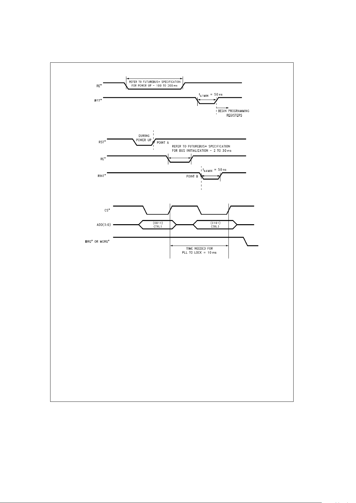
10.0 Reset/Initialization/Power Up (Continued)
TL/H/10747– 25
FIGURE 10a. Programming Registers: After Power-Up
TL/H/10747– 26
FIGURE 10b. Programming Registers: During Bus Initialization
TL/H/10747– 27
FIGURE 10c. PLL Lock Period
11.0 Live Insertion
The arbitration Controller supports live insertion (see
Figure
11
). When a module is being live inserted into an active
Futurebus
a
system it will be powered up and reset. The
live inserted module will reset it’s arbitration controller with
the RST* input and will drive re* on the Futurebus
a
back-
plane.
RE* asserted will cause all active Futurebus
a
modules to
release their bus lines to prepare for live insertion to the
Futurebus
a
backplane.
When all the active Futurebus
a
modules detect RE* asserted, they should assert HALT* to their arbitration controller and limit the current parallel bus transaction to 128 ms.
The active modules will then remain in Phase 0, upon completion of the current control acquisition cycle, until HALT*
is negated.
When the live inserted module detects both:
1. the Parallel bus in the Idle state (AS* and AKf negated),
2. the arbitration bus lines in Phase 0
for 1 ms then it should assert ai* (protocol controller) and
negate the RST* input. The arbitration controller will assert
ARO upon detecting the negation of RST*. These actions
will complete the Futurebus
a
alignment. The live inserted
module will then be in arbitration Phase 0; thus, aligned with
the other live modules. Then the live inserted module will
negate re*.
When the active modules detect the negation of RE* they
negate the HALT* input to their arbitration controllers, thus
allowing arbitration competition to proceed.
At this point, the live inserted module can only participate as
a by-stander during the arbitration competition cycle until it
is programmed and 10 ms has elapsed (PLL lock on time).
Once the 10 ms has elapsed the module can enable arbitration competition by setting the GO bit in CTRL3. At this time
bus requests (BRQ*, MGRQ*) can be accepted to join competition for the parallel bus.
41
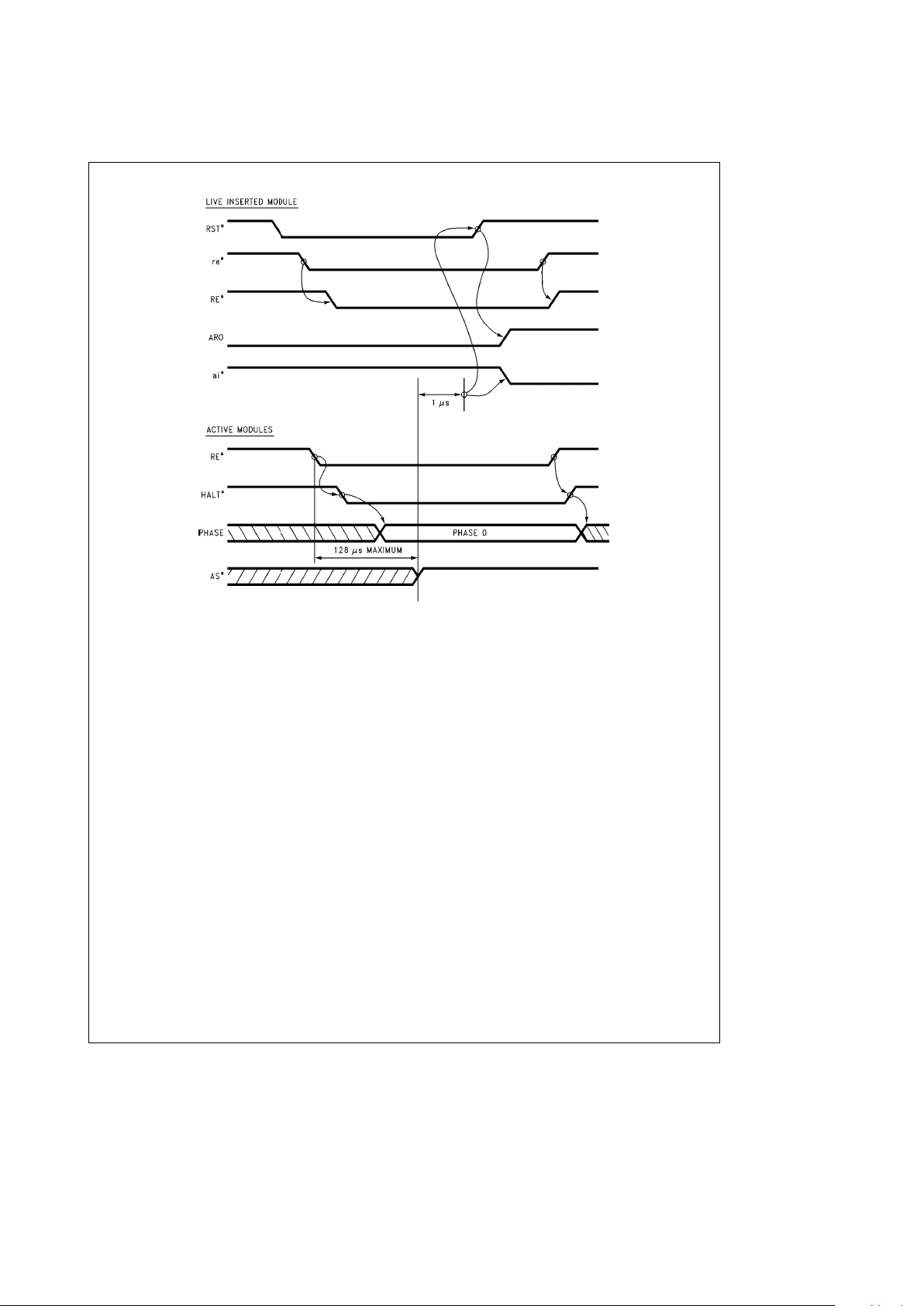
11.0 Live Insertion (Continued)
TL/H/10747– 28
FIGURE 11. Live Insertion
12.0 Live Withdrawal
When a module is notified to be live withdrawn it will:
1. complete any tasks currently in progress
2. inhibit itself from participating in any more bus transactions (becomes a by-stander)
The module can withdraw from the arbitration protocol in
one of three phases:
1. During phase 0 by negating ARO
2. During phase 2 by negating APO
3. During phase 4 by negating AQO
This may be achieved in the DS3875 by issuing the HALT*
signal, then when it is observed that the arbitration controller is in Phase 0, asserting the RST* signal to cause all
outputs of the arbitration bus to be released. The module
may then be withdrawn from the Futurebus
a
system.
13.0 Testing the DS3875
The Arbitration Controller has features designed in which
ease the testing and monitoring tasks for the user. Registers may be read to determine proper functionality of the
chip. For instance, while the Arbitration Controller is operat-
ing, the arbitration phase can be monitored by reading the
state register. Also to check proper operation of the 1 ms
timer, divide by n divider, and divide by 40 divider, the
TCSEL bit in CTRL3 register can be set so that a test clock
may be used. This will allow the clock signal to be applied to
the circuitry, thus disabling the internally generated signals
that are used during normal operation. See
Figure 10
.To
determine the status of the timer and dividers, the status
register CT(0:2) bits can be read.
If the user wants to check the proper operation of the CN
port:
1. An arbitration number can be loaded into the CN port by
performing a write cycle to any of the receive registers
(RXCN0, RXCN1, or RXMSG). The Arbitration Controller
will load the number from the CN port instead of the
DATA port into the register upon detecting a write to any
of the receive registers. The timing is the same as those
given for the register write using the DATA port. Refer to
Timing Section T2.
2. Next, by performing a read cycle to the register just writ-
ten to (RXCN0, RXCN1, or RXMSG), the arbitration number stored will be placed onto the DATA port. Thus, the
proper operation of the CN port is tested.
42

14.0 Electrical Characteristics
Absolute Maximum Ratings
If Military/Aerospace specified devices are required,
please contact the National Semiconductor Sales
Office/Distributors for availability and specifications.
Supply Voltage 6.5V
Control Input Voltage 5.5V
Power Dissipation at 70
§
C 0.6W
Storage Temperature Range
b
65§Ctoa150§C
Lead Temperature 260
§
C
Recommended Operating
Conditions
Min Max Units
Supply Voltage, V
DD
4.5 5.5 V
Operating Free Air Temperature 0 70 C
ESD Tolerance:
C
ZAP
e
120 pF, R
ZAP
e
1500X 2kV
Electrical Characteristics (Notes 2 and 3) T
A
e
0§Ctoa70§C, V
CC
e
5Vg10%
Symbol Parameter Conditions Min Typ Max Units
V
IH
Minimum Input High Voltage 2.8 V
V
IL
Minimum Input Low Voltage 0.8 V
V
OH
Voltage Output High IOH,IOLfor Several Drivers
2.4 3.2 V
i.e., I
OL
4mA
V
OL
Voltage Output Low IOH,IOLfor Several Drivers
0.35 0.5 V
i.e., IOL8mA
I
I
Input Leakage Current Input at VDDor V
SS
b
1.0 1.0 mA
I
IH
Input High Current Input at V
IH
1.0 mA
I
IL
Input Low Current Input at V
IL
b
1.0 mA
I
DD
Supply Current Dynamic Supply Current 100 mA
I
CC
Static Supply Current Input at Standby 30 mA
Note 1: ‘‘Absolute maximum ratings’’ are those beyond which the safety of the device cannot be guaranteed. They are not meant to imply that the device should be
operated at these limits. The table of ‘‘Electrical Characteristics’’ provide conditions for actual device operation.
Note 2: All currents into device pins are positive; all currents out of device pin are negative. All voltages are referenced to device ground unless otherwise
specified.
Note 3: All typicals are given for V
DD
e
5V, and T
A
e
25§C.
15.0 AC Parameters
Legend to AC Parameter Number Assignments
Parameter
Description
Number
t000–t099 Phase 0
t100–t199 Phase 1
t200–t299 Phase 2
t300–t399 Phase 3
t400–t499 Phase 4
t500–t599 Phase 5
tAXX Reset, Initialization
tBXX Register Access Data Port
tCXX Register Access CN Port - Input
tDXX Clearing Interrupts
tEXX FIFO Strobe
tFXX WIN*ÐGT* Valid
tGXX Message Signals
tHXX Busrequest, Busgrant, End of Tenure
tJXX Locked, Unlock Handshake Signals
43

15.0 AC Parameters (Continued)
AC Timing Parameters Unless otherwise stated: T
A
e
0§Ctoa70§C, V
CC
e
5Vg10%
All transitions are specified after the input signals are stable and valid for evaluation. This table will describe the
parameters as given in the following pages. All values are given in nanoseconds (ns), unless otherwise stated.
Number Symbol Parameter Description Min Typ Max
t1t
BQBG
BRQ* Asserted to BGRNT* Asserted 19 33
t2t
AQAC
AQI Negated to AC0O, AC1O Negated 22 30
t3t
APIO
API Asserted to APO Asserted 16 26
t4t
RQAP
MGRQ* or BRQ* Asserted to APO Asserted 19 32
t5t
EDAP
(Dummy Cycle) ENDT* Asserted to APO Asserted 28 40
t6t
BQAP
(Consecutive Bus Requests) BRQ* Asserted to APO Asserted 17 28
t7t
HTAP
HALT* Negated to APO Asserted 16 26
t
100tCNLEAR
CNÐLE* Negated to ARO Negated. Determined by Programmable 2a(0b25) 4a(0b25)
Value
t
101tCNLE
CNÐLE* Width 18 20 26
t
102tCNS
CN Port Setup Time 23 28
t
103tCNZ
ARI Negated to TRI-STATE CN Port 16 20
t
104tIBCAR
(IBA Mode) IBA-CMPT* Asserted to ARO Negated. Determined by 20a(0b25) 30a(0b25)
Programmable Value
t
105tCPTAR
CMPT* Asserted to ARO Negated. Determined by Programmable 20a(0b25) 30a(0b25)
Value
t
106tAC0AR
(Slow Mode) AC0O Asserted to ARO Negated. Determined by 20a(0b25) 30a(0b25)
Programmable Value
t
107tAPCNLE
APO Asserted to CN-LE* Asserted. CTRL3[0], ‘‘G0’’ Bit is Set 22 32
t
108tAPCPTA
APO Asserted to CMPT* Asserted 14 22
t
109tAPIBC
APO Asserted to IBAÐCMPT* Asserted 13 18
t
110tAPAC
APO Asserted to AC0O Asserted (Slow Mode) 18 28
t
200tARABRD
ARI Negated to ABÐRE* Asserted 52 62
t
201tARIBS
(IBA Mode) ARI Negated to IBAÐS*.T
A
e
Arbitration Timer 60–300 T
A
T
A
t
202tIBSBG
(IBA Mode) IBAÐS* Asserted to BGRNT* Asserted 19 33
t
203tWINAQ
WIN*ÐGT* Asserted to AQO Asserted. After TAExpired. 18 29
t
204tAQIO
AQI Asserted to AQO Asserted 13 20
t
205tARAQ
ARI Negated to AQO Asserted 18aT
A
28aT
A
t
207tIBSAQ
(IBA Mode) IBA-S* Asserted to AQO Asserted 20 33
t
300tAC10AP
AC10 Asserted to APO Negated 15 29
t
301tASNAP
ASÐCancel* Negated to APO Negated 15 24
t
310tAPABRD
APO Negated to ABÐRE* Negated 5 8
t
320tAQAC1
AQO Asserted to AC1O Asserted 6 10
t
321tAC1IAPN
AC1I Asserted to APO Negated 7 12 18
t
322tASAAP
ASÐCancel* Asserted to APO Negated 7 12 18
t
330tAC1IAP
AC1I Asserted to APO Negated 13 22
t
340tRQAC
MGRQ* or BRQ* Negated to AC0O, AC1O Asserted 21 32
t
341tAQAC0
AQO Asserted to AC0O Negated 0 3
t
342tAQER
AQO Asserted to ERIT* Asserted 14 22
t
400tAPCPTN
API Negated to CMPT* Negated 18 30
44

15.0 AC Parameters (Continued)
AC Timing Parameters Unless otherwise stated: T
A
e
0§Ctoa70§C, V
CC
e
5Vg10% (Continued)
All transitions are specified after the input signals are stable and valid for evaluation. This table will describe the
parameters as given in the following pages. All values are given in nanoseconds (ns), unless otherwise stated.
Number Symbol Parameter Description Min Typ Max
t
401tAC1IAR
AC1I Asserted to ARO Asserted 12 21
t
403tCANAC1
ASÐCancel* Asserted to AC1O Asserted 7 19
t
405tARIO
ARI Asserted to ARO Asserted 14 19
t
407tEDAR
ENDT* Asserted to ARO Asserted 15 25
t
500tARBG
ARO Asserted to BGRNT* Asserted 7 12
t
501tOAQ
BGRNT*, MGTX*, UNLK* or any Interrupt Asserted to AQO Negated 5 7
t
502tARFTR
ARO Asserted to FSTR* Negated 5 8
t
503tARIBC
ARO Asserted to IBAÐCMPT* Negated 5 8
t
504tARABSA
ARO Asserted to MGTX*, UNLK* or any Interrupt Asserted 5 9
t
A1tRSTPW
RST* Pulse Width 50 50
t
A2tRSTRE
Output Reset Time 30 45
t
A3tRSTAR
RST* Negated to ARO Asserted 15 25
t
A4tRINTPW
RINT* Pulse Width 50 50
t
A5tRINTRE
Output Initialization Reset Time 30 45
t
B1tCSPW
CS* Pulse Width 35
t
B2tCSPWN
CS* Recovery Time 15
t
B3tCSDKA
CS* Asserted to DSACK* Asserted 12 18
t
B4tADDS
ADD (3:0) Setup Time 52
tB5t
ADDH
ADD (3:0) Hold Time 65
tB6t
CSDKN
CS* Negated to DSACK* Negated 7 12
t
B7tRWS
RÐW* Setup Time 0
t
B8tSELS
SEL Setup Time 0
t
B10tDATASDK
Data (7:0) Setup Time with Respect to DSACK* 24 15
t
B11tDATAHDK
Data (7:0) Hold Time with Respect to DSACK* 00
t
B12tSELH
SEL Hold Time 3
t
B24tDATASCS
Data (7:0) Setup Time with Respect to CS* Negated 15 6
t
B25tDATAHCS
Data (7:0) Hold Time with Respect to CS* Negated 5 5
t
B27tDATALZ
Data (7:0) Low Z Time 14 22
t
B28tDATAV
Data (7:0) Valid Time before DSACK*
t
B29tDATAA
Data (7:0) Access Time with Respect to CS* Asserted 22 30
t
B30tDATAHRC
Data (7:0) Hold Time 610
t
B31tDATAHZ
Data (7:0) Hi–Z Time 12 25
t
C2tABRDCNZ
ABÐRE* Negated to CN (7:0) TRI-STATE 0 0
t
D1tCSXINTN
CS* Asserted to any Interrupt Negated 22 36
t
E1tFSTR
FSTR* Recovery Time 80
45
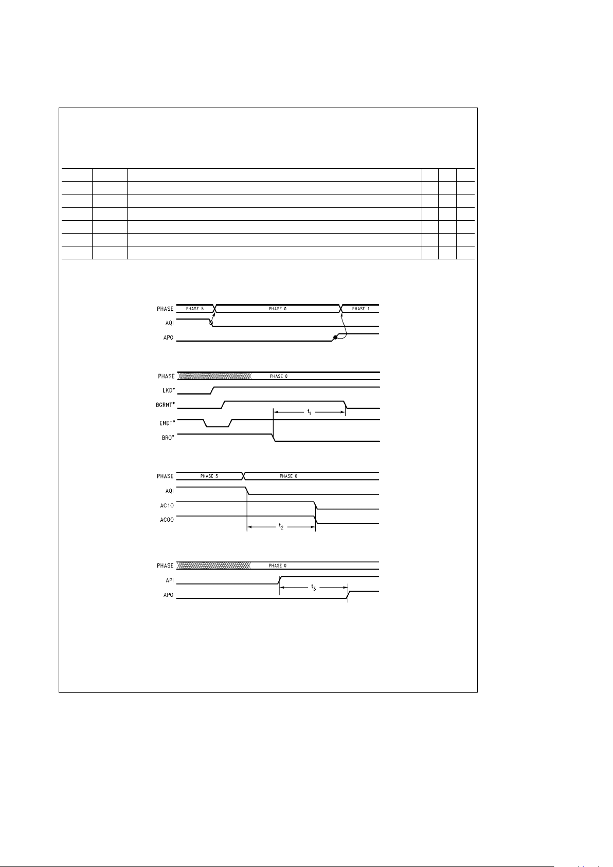
15.0 AC Parameters (Continued)
AC Timing Parameters Unless otherwise stated: T
A
e
0§Ctoa70§C, V
CC
e
5Vg10% (Continued)
All transitions are specified after the input signals are stable and valid for evaluation. This table will describe the
parameters as given in the following pages. All values are given in nanoseconds (ns), unless otherwise stated.
Number Symbol Parameter Description Min Typ Max
tE2t
FSTABRD
ABÐRE* High Time with Respect to FSTR* 60
tF1t
WINALL1
ALL1* Asserted with Respect to WIN*ÐGT* 5
tF2t
WINPER
PER* Asserted with Respect to WIN*ÐGT* 5
t
G1tMGXN
MGRQ* Negated to MGTX* Negated 14 22
t
H2tEDBGN
ENDT* Asserted to BGRNT* Negated 17 25
tJ1t
LKULKN
LKD* Negated to UNLK* Negated 12 18
Phase 0 Timing
A. Transitioning Into and Out of Phase 0
TL/H/10747– 31
B. Parking (Assume ! IBAÐPK*)
TL/H/10747– 32
C. Negating AC10 and AC00 When Entering Phase 0
TL/H/10747– 33
D. Another Module Initiating Competition
TL/H/10747– 34
46
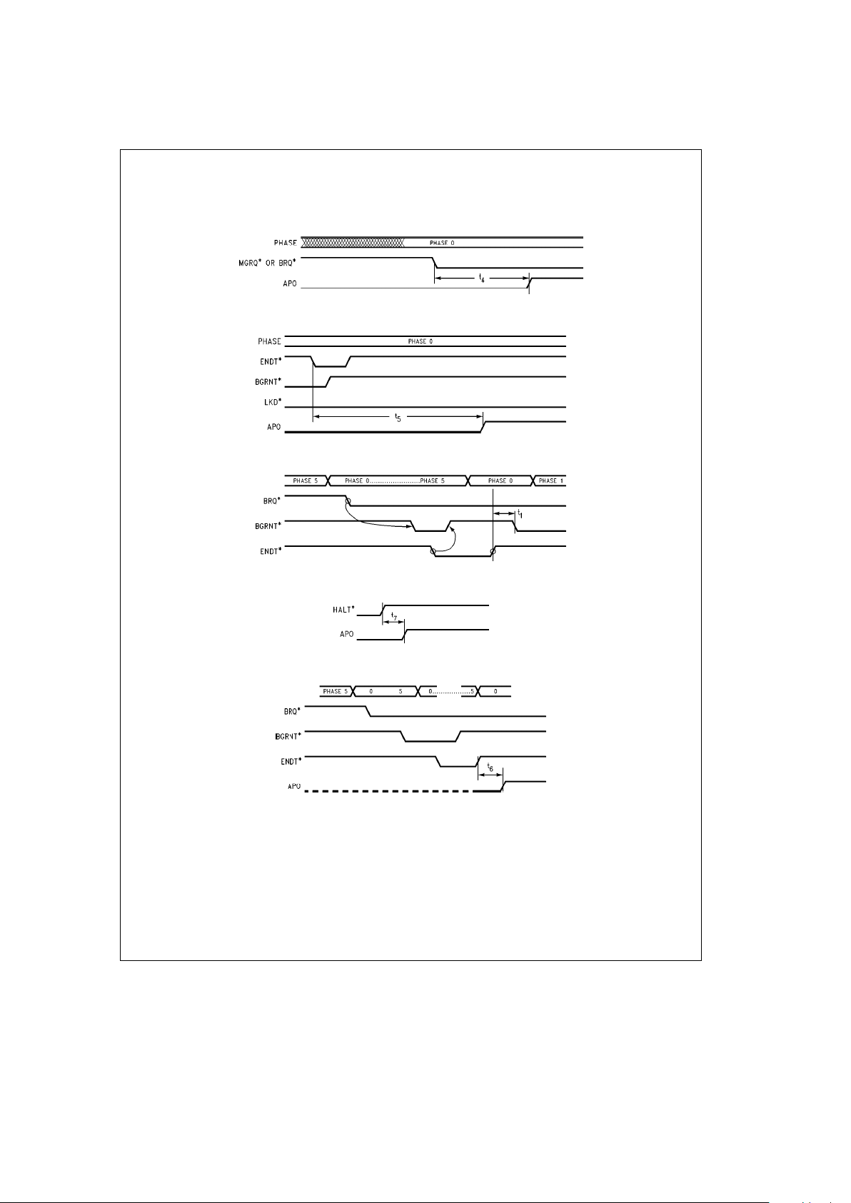
15.0 AC Parameters (Continued)
Phase 0 Timing (Continued)
E. Message Request or Bus Request Initiating Competition
TL/H/10747– 35
F. Dummy Cycle to Generate Unlock (! UNLK*) During Phase 5
TL/H/10747– 36
G. Consecutive Bus Requests: Parking
TL/H/10747– 37
H. HALT* Release
TL/H/10747– 75
I. Consecutive Bus Requests: Non-Parking
TL/H/10747– 78
47

15.0 AC Parameters (Continued)
Phase 1 Timing
TL/H/10747– 38
C. IBA Mode Selected
TL/H/10747– 39
D. Competing
TL/H/10747– 40
E. Asserting AC0O - Slow Mode (FÐS*) is Selected
TL/H/10747– 41
48

15.0 AC Parameters (Continued)
Phase 2 Timing
A. Transitioning Into and Out of Phase 2
TL/H/10747– 42
B. Register Access CN Port–Input
TL/H/10747– 43
C. IBA Mode Selected–Winner of Competition
TL/H/10747– 44
E. Bystander
TL/H/10747– 45
49

15.0 AC Parameters (Continued)
Phase 3 Timing
A. Transitioning Into and Out of Phase 3
TL/H/10747– 46
B. AS Low and No Errors
TL/H/10747– 47
C. Reading the Winning Competition Number (! ABÐRE*)
TL/H/10747– 48
D. Successful IBA Competition Timing
TL/H/10747– 49
E. Transfer of Tenure Inhibited
TL/H/10747– 50
50

15.0 AC Parameters (Continued)
Phase 3 Timing (Continued)
F. Message Request or Bus Request Being Negated During Phase 3 (If This Module was the Winner)
TL/H/10747– 51
G. Second Pass Required
TL/H/10747– 52
H. Slow Case ACO Recovery
TL/H/10747– 76
Phase 4 Timing
A. Transitioning Into and Out of Phase 4
TL/H/10747– 53
B. Complete Signal is Negated
TL/H/10747– 54
C. Inhibit Transfer of Tenure
TL/H/10747– 55
51

15.0 AC Parameters (Continued)
Phase 4 Timing (Continued)
D. Module (Except Master Module) Receives ARI
TL/H/10747– 56
E. End of Tenure
TL/H/10747– 57
Phase 5 Timing
A. Transitioning Into and Out of Phase 5
TL/H/10747– 58
B. Master Elect Gets Bus Grant When No Errors Occurred
TL/H/10747– 59
C. Message was Transmitted (During 2nd Pass–No Errors Occurred),
Generation of Interrupt Signal, PFINT*, or MGINT*,
Generation of Unlock Signal When Locked (! LKD*)
TL/H/10747– 60
D. FIFO Strobe
TL/H/10747– 61
E. Release of IBAÐCMPT*
TL/H/10747– 77
52

15.0 AC Parameters (Continued)
T1a. RST* Signal
TL/H/10747– 62
T1b. RINT* Signal
TL/H/10747– 63
T2a. Register Access DATA Port– WRITE CYCLE USING DSACK*
TL/H/10747– 64
53

15.0 AC Parameters (Continued)
T2b. Register Access DATA Port–Write CYCLE Using CS*
TL/H/10747– 65
T2c. Register Access DATA Port–Read CYCLE
TL/H/10747– 66
54
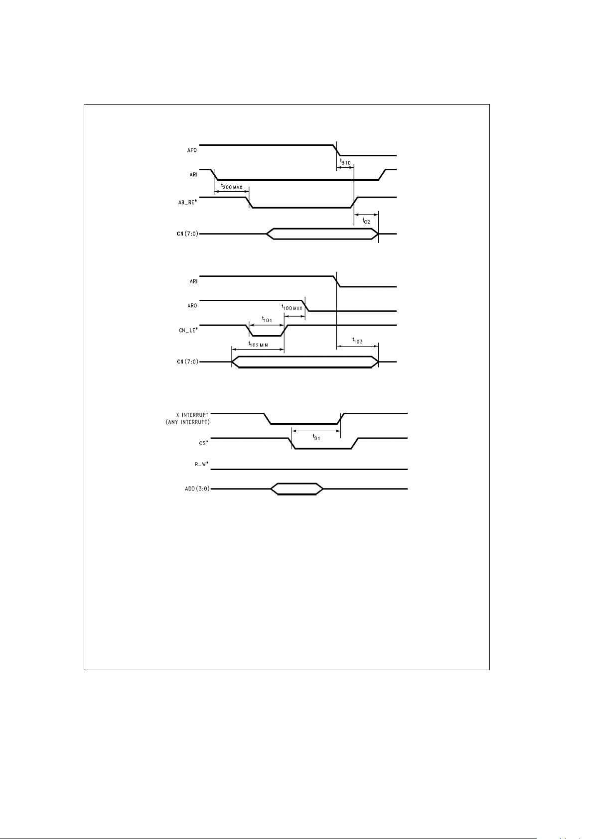
15.0 AC Parameters (Continued)
T3. Register Access CN Port–Input
TL/H/10747– 67
T4. Register Access CN Port–Output
TL/H/10747– 68
These sections are shown to give a better understanding of the CN port timing. Most of the parameters are given under the phase timing diagrams. Also a few
parameters are added here to these diagrams.
T5. Clearing Interrupts
TL/H/10747– 69
55

15.0 AC Parameters (Continued)
T6. FIFO Strobe
TL/H/10747– 70
T7. WIN*ÐGT* Valid
TL/H/10747– 71
T8. Compete Signal
TL/H/10747– 72
These sections give some additional parameters, these are not the complete set of parameters specified for these signals. Also refer to the phase timing
diagrams.
56

15.0 AC Parameters (Continued)
T10. BUSREQUEST, BUSGRANT and END of TENURE HANDSHAKE
TL/H/10747– 73
T11. LKD* and UNLK* Handshake Signals
TL/H/10747– 74
57

DS3875 Futurebus
a
Arbitration Controller
Physical Dimensions inches (millimeters)
Order Number DS3875V
NS Package V68A
LIFE SUPPORT POLICY
NATIONAL’S PRODUCTS ARE NOT AUTHORIZED FOR USE AS CRITICAL COMPONENTS IN LIFE SUPPORT
DEVICES OR SYSTEMS WITHOUT THE EXPRESS WRITTEN APPROVAL OF THE PRESIDENT OF NATIONAL
SEMICONDUCTOR CORPORATION. As used herein:
1. Life support devices or systems are devices or 2. A critical component is any component of a life
systems which, (a) are intended for surgical implant support device or system whose failure to perform can
into the body, or (b) support or sustain life, and whose be reasonably expected to cause the failure of the life
failure to perform, when properly used in accordance support device or system, or to affect its safety or
with instructions for use provided in the labeling, can effectiveness.
be reasonably expected to result in a significant injury
to the user.
National Semiconductor National Semiconductor National Semiconductor National Semiconductor
Corporation Europe Hong Kong Ltd. Japan Ltd.
1111 West Bardin Road Fax: (
a
49) 0-180-530 85 86 13th Floor, Straight Block, Tel: 81-043-299-2309
Arlington, TX 76017 Email: cnjwge@tevm2.nsc.com Ocean Centre, 5 Canton Rd. Fax: 81-043-299-2408
Tel: 1(800) 272-9959 Deutsch Tel: (
a
49) 0-180-530 85 85 Tsimshatsui, Kowloon
Fax: 1(800) 737-7018 English Tel: (
a
49) 0-180-532 78 32 Hong Kong
Fran3ais Tel: (
a
49) 0-180-532 93 58 Tel: (852) 2737-1600
Italiano Tel: (
a
49) 0-180-534 16 80 Fax: (852) 2736-9960
National does not assume any responsibility for use of any circuitry described, no circuit patent licenses are implied and National reserves the right at any time without notice to change said circuitry and specifications.
 Loading...