

NSC DS3862WMX, DS3862WM, DS3862N Datasheet
DS3862
Octal High Speed Trapezoidal Bus Transceiver
General Description
The DS3862 is an octal high speed schottky bus transceiver
intended for use with terminated 120Ω impedance lines. It is
specifically designed to reduce noise in unbalanced transmission systems. The open collector drivers generate precise trapezoidal waveforms with rise and fall times of 9 ns
(typical), which are relatively independentofcapacitiveloading conditions on the outputs. This reduces noise coupling to
the adjacent lines without any appreciable impact on the
maximum data rate obtainable with high speed bus transceivers. In addition, the receivers use a low pass filter in conjunction with a high speed comparator, to further enhance
the noise immunity. Tightly controlled threshold levels on the
receiver provide equal rejection to both negative and positive
going noise pulses on the bus.
The external termination is intended to be a 180Ω resistor
from the bus to 5V logic supply, together with a 390Ω resistor
from the bus to ground. The bus can be terminated at one or
both ends.
Features
n Guaranteed A.C. specifications on noise immunity and
propagation delay over the specified temperature and
supply voltage range
n Temperature insensitive receiver thresholds track bus
logic level and respond symmetrically to positive and
negative going pulses
n Trapezoidal bus waveforms reduce noise coupling to
adjacent lines
n Open collector driver output allows wire-or connection
n Advanced low power schottky technology
n Glitch free power up/down protection on driver and
receiver outputs
n TTL compatible driver and control inputs, and receiver
outputs
n Control logic is the same as the DS3896
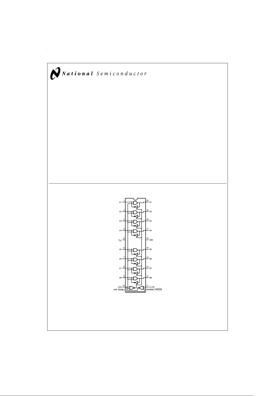
Logic and Connection Diagram
DS008539-1
Order Number DS3862J, DS3862N or DS3862WM
See NS Package Number J20A, N20A or M20B
February 1995
DS3862 Octal High Speed Trapezoidal Bus Transceiver
© 1999 National Semiconductor Corporation DS008539 www.national.com
Absolute Maximum Ratings (Note 1)
If Military/Aerospace specified devices are required,
please contact the National Semiconductor Sales Office/
Distributors for availability and specifications.
Supply Voltage 6V
Control Input Voltage 5.5V
Driver Input and Receiver Output 5.5V
Receiver Input and Driver Output 5.5V
Power Dissipation 1400 mW
Storage Temperature Range −65˚C to +150˚C
Lead Temperature (Soldering, 4 seconds) 260˚C
Recommended Operating
Conditions
Min Max Units
Supply Voltage,V
CC
4.75 5.25 V
Operating Free Air Temperature 0 70 ˚C
Electrical Characteristics (Notes 2, 3)
0˚C ≤ TA≤ 70˚C, 4.75V ≤ VCC≤ 5.25V unless otherwise specified
Symbol Parameter Conditions Min Typ Max Units
Driver and Control Inputs:
V
IH
Logical “1” Input Voltage 2.0 V
V
IL
Logical “0” Input Voltage 0.8 V
I
I
Logical “1” Input Current An=V
CC
1mA
I
IH
Logical “1” Input Current An=2.4V 40 µA
I
IHC
Logical “1” Input Current CD=T/R=2.4V 80 µA
I
IL
Logical “0” Input Current An=0.4V −1 −1.6 mA
I
ILC
CD & T/R Logical “0” Input Current CD=T/R=0.4V −180 −400 µA
V
CL
Input Diode Clamp Voltage Iclamp=−12 mA −0.9 −1.5 V
Driver Output/Receiver Input
V
OLB
Low Level Bus Voltage An=T/R=2V, Ibus=100 mA 0.6 0.9 V
I
IHB
Logical “1” Bus Current An=0.8V, Bn=4V, V
CC
=
5.25V and 0V 10 100 µA
I
ILB
Logical “0” Bus Current An=0.8V, Bn=0V, V
CC
=
5.25V and 0V 100 µA
V
TH
Input Threshold V
CC
=
5V 1.5 1.7 1.9 V
Receiver Output
V
OH
Logical “1” Output Voltage Bn=0.9V, I
oh
=
− 400µA 2.4 3.2 V
V
OL
Logical “0” Output Voltage Bn=4V, I
ol
=
16 mA 0.35 0.5 V
I
OS
Output Short Circuit Current Bn=0.9V −20 −70 −100 mA
I
CC
Supply Current V
CC
=
5.25V 90 135 mA
Note 1: “Absolute Maximum Ratings” are those beyond which the safety of the device cannot be guaranteed. They are not meant to imply that device should be operated at these limits. The table of “Electrical Characteristics” provide conditions for actual device operation.
Note 2: All currents into device pins are positive; all currents out of device pins are negative. All voltages are referenced to device ground unless otherwise specified.
Note 3: All typicals are given for V
CC
=
5V and T
A
=
25˚C.
Switching Characteristics
0˚C ≤ TA≤ 70˚C, 4.75V ≤ VCC≤ 5.25V unless otherwise specified
Symbol Parameter Conditions Min Typ Max Units
Driver:
t
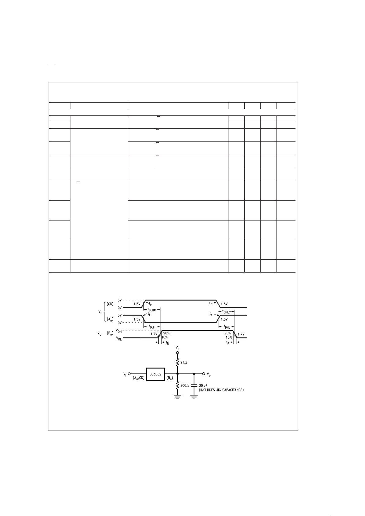
DLH
An to Bn CD=0.8V, T/R=2.0V, VL=5V (
Figure 1
) 12 20 ns
t
DHL
12 20 ns
t
DLHC
CD to Bn An=T/R=2.0V, VL=5V, (
Figure 1
) 12 20 ns
t
DHLC
15 25 ns
t
DLHT
T/R to Bn VCI=An, VC=5V, (
Figure 2
)2030ns
t
DHLT
CD=0.8V, RC=390Ω,CL=30 pF 25 40 ns
RL1=91Ω, RL2=200Ω,VL=5V
t
R
Driver Output Rise Time CD=0.8V, T/R=2V, VL=5V (
Figure 1
) 4 9 20 ns
t
F
Driver Output Fall Time 4 9 20 ns
www.national.com 2
Switching Characteristics (Continued)
0˚C ≤ TA≤ 70˚C, 4.75V ≤ VCC≤ 5.25V unless otherwise specified
Symbol Parameter Conditions Min Typ Max Units
Receiver:
t
RLH
Bn to An CD=0.8V, T/R=0.8V (
Figure 3
) 15 25 ns
t
RHL
15 25 ns
t
RLZC
CD to An Bn=2.0V, T/R=0.8V, CL=5pF 15 25 ns
RL1=390Ω, RL2=NC, VL=5V (
Figure 4
)
t
RZLC
Bn=2.0V, T/R=0.8V, CL=30 pF 10 20 ns
RL1=390Ω, RL2=1.6K, VL=5V (
Figure 4
)
t
RHZC
Bn=0.8V, T/R=0.8V, VL=0V, 510 ns
RL1=390Ω, RL2=NC, CL=5pF (
Figure 4
)
t
RZHC
Bn=0.8V, T/R=0.8V, VL=0V, 815 ns
RL1=NC, RL2=1.6K, CL=30 pF (
Figure 4
)
t
RLZT
T/R to An VCI=Bn, VC=3.4V, RC=39Ω 20 30 ns
CD=0.8V, VL=5V, RL1=390Ω,
RL2=NC, CL=5pF (
Figure 2
)
t
RZLT
VCI=Bn, VC=3.4V, RC=39Ω,3045ns
CD=0.8V, VL=5V, RL1=390Ω,
RL2=1.6K, CL=30 pF (
Figure 2
)
t
RHZT
VCI=Bn, VC=0V, RC=39Ω 510 ns
CD=0.8V, VL=0V, RL1=390Ω,
RL2=NC, CL=5pF (
Figure 2
)
t
RZHT
VCI=Bn, VC=0V, RC=39Ω,1020ns
CD=0.8V, VL=0V, RL1=NC
RL2=1.6K, CL=30 pF (
Figure 2
)
t
NR
Receiver Noise Rejection (
Figure 5
) 9 12 ns
Pulse Width
Note: NC means open
Switching Waveforms
DS008539-2
Note: t
r
=
t
f
≤ 5 ns from 10%to 90
%
FIGURE 1. Driver Propagation Delays
www.national.com3
 Loading...