

DS16F95, DS36F95
EIA-485/EIA-422A Differential Bus Transceiver
General Description
The DS16F95/DS36F95 Differential Bus Transceiver is a
monolithic integrated circuit designed for bidirectional data
communication on balanced multipoint bus transmission
lines. The transceiver meets both EIA-485 and EIA-422A
standards.
The DS16F95/DS36F95 offers improved performance due to
the use of L-FAST bipolar technology. The L-FAST technology allows forhigher speeds and lower currents by minimizing gate delay times. Thus, the DS16F95andDS36F95 consume less power, and feature an extended temperature
range as well as improved specifications.
The DS16F95/DS36F95 combines a TRI-STATE
®
differential line driver and a differential input line receiver, both of
which operate from a single 5.0V power supply. The driver
and receiver have an active Enable that can be externally
connected to function as a direction control. The driver differential outputs and the receiver differential inputs are internally connected to form differential input/output (I/O) bus
ports that are designed to offer minimum loading to the bus
whenever the driver is disabled or when V
CC
= 0V. These
ports feature wide positive andnegative common mode voltage ranges, making the device suitable for multipoint applications in noisy environments.
The driver is designed to accommodate loads of up to 60 mA
of sink or source current and features positive and negative
current limiting in addition to thermalshutdown for protection
from line fault conditions.
The DS16F95/DS36F95 can be used in transmission line
applications employing the DS96F172 and the DS96F174
quad differential line drivers and the DS96F173 and
DS96F175 quad differential line receivers.
Features
n Meets EIA-485 and EIA-422A
n Meets SCSI-1 (5 MHZ) specifications
n Designed for multipoint transmission
n Wide positive and negative input/output bus voltage
ranges
n Thermal shutdown protection
n Driver positive and negative current-limiting
n High impedance receiver input
n Receiver input hysteresis of 50 mV typical
n Operates from single 5.0V supply
n Reduced power consumption
n Pin compatible with DS3695 and SN75176A
n Military temperature range available
n Qualified for MIL-STD 883C
n Standard Military Drawings (SMD) available
n Available in DIP (J), SOIC (M), LCC (E), and Flatpak
(W) packages
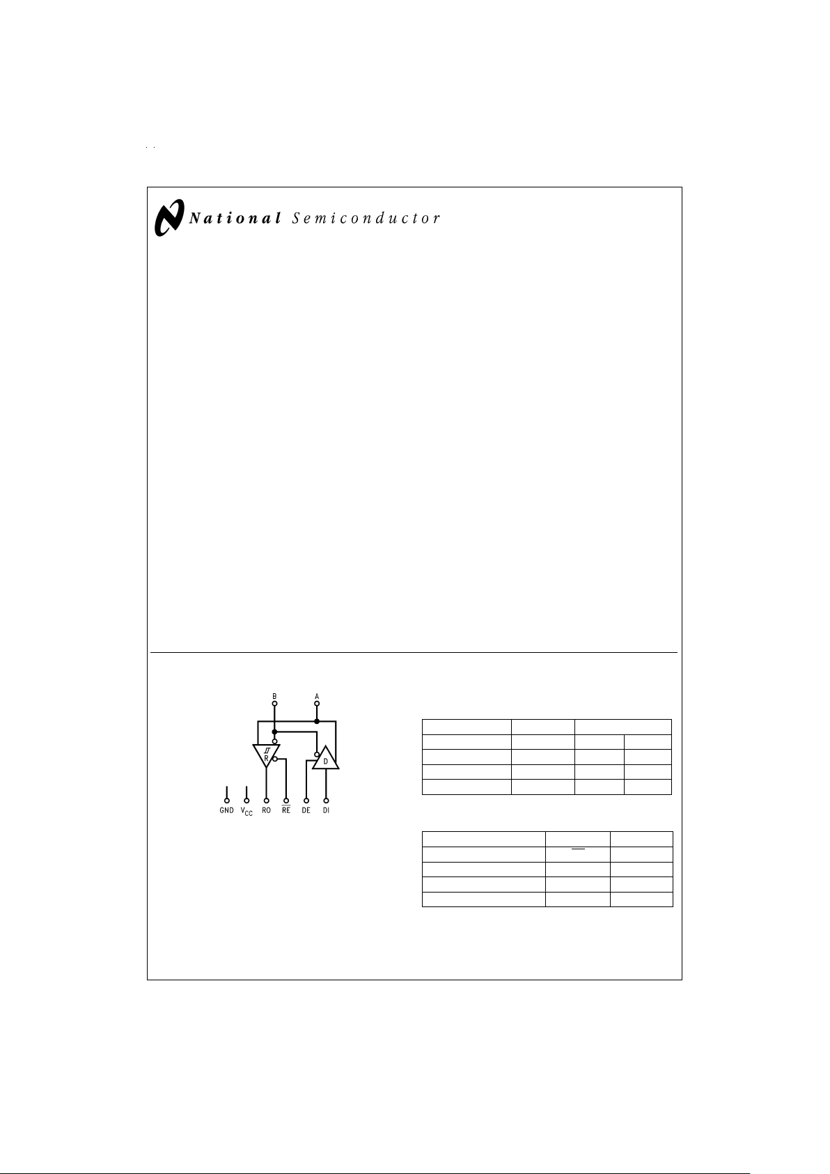
Logic Diagram Function Tables
Driver
Driver Input Enable Outputs
DI DE A B
HHHL
LHLH
XLZZ
Receiver
Differential Inputs Enable Output
A–B RE
RO
V
ID
≥ 0.2V L H
V
ID
≤ −0.2V L L
XHZ
H = High Level
L = Low Level
X = Immaterial
Z = High Impedance (Off)
TRI-STATE®is a registered trademark ofNational Semiconductor Corporation.
DS009629-20
June 1998
DS16F95, DS36F95 EIA-485/EIA-422A Differential Bus Transceiver
© 1998 National Semiconductor Corporation DS009629 www.national.com
COMMERCIAL
Absolute Maximum Ratings
(Note 2)
Specifications for the 883 version of this product are
listed separately on the following pages.
Storage Temperature Range −65˚C to +175˚C
Lead Temperature
(Soldering, 60 sec.) 300˚C
Maximum Package Power Dissipation (Note 1) at 25˚C
’J’ Package 1300 mW
’M’ Package 735 mW
Supply Voltage 7.0V
Input Voltage (Bus Terminal) +15V/−10V
Enable Input Voltage 5.5V
Recommended Operating
Conditions
Min Typ Max Units
Supply Voltage (V
CC
)
DS36F95 4.75 5.0 5.25 V
DS16F95 4.50 5.0 5.50 V
Voltage at Any Bus Terminal
(Separately or Common Mode)
(V
I
or VCM) −7.0 +12 V
Differential Input
±
12 V
Voltage (V
ID
)
Output Current HIGH (I
OH
)
Driver −60 mA
Receiver −400 µA
Output Current LOW (I
OL
)
Driver 60 mA
Receiver 16 mA
Operating Temperature (T
A
)
DS36F95 0 +25 +70 ˚C
DS16F95 −55 +25 +125 ˚C
Note 1: Derate ’J’ package 8.7 mW/˚C above 25˚C.
Derate ’M’ package 5.88 mW/˚C above 25˚C.
Driver Electrical Characteristics (Notes 3, 4)
Over recommended supply voltage and operating temperature ranges, unless otherwise specified
Symbol Parameter Conditions Min Typ Max Units
V
IH
Input Voltage HIGH 2.0 V
V
IL
Input Voltage LOW 0.8 V
V
OH
Output Voltage HIGH IOH= −55 mA 0˚C to +70˚C 3.0 V
V
OL
Output Voltage LOW IOL= 55 mA 0˚C to +70˚C 2.0 V
V
IC
Input Clamp Voltage II= −18 mA −1.3 V
|V
OD1
| Differential Output Voltage IO= 0 mA 6.0 V
|V
OD2
| Differential Output Voltage RL= 100Ω,
Figure 1
2.0 2.25 V
R
L
=54Ω,
Figure 1
1.5 2.0
∆|V
OD
| Change in Magnitude of RL=54Ωor 100Ω, −40˚C to +125˚C
±
0.2 V
Differential Output Voltage
Figure 1
−55˚C to +125˚C
±
0.4
(Note 5)
V
OC
Common Mode Output
Voltage (Note 6)
3.0 V
∆|V
OC
| Change in Magnitude of
Common Mode Output
Voltage (Note 5)
±
0.2 V
I
O
Output Current (Note 9) Output Disabled VO= +12V 1.0 mA
(Includes Receiver I
I
)V
O
= −7.0V −0.8
I
IH
Input Current HIGH VI= 2.4V 20 µA
I
IL
Input Current LOW VI= 0.4V −50 µA
I
OS
Short Circuit Output Current
(Note 10)
VO= −7.0V −250
V
O
= 0V −150 mA
V
O=VCC
150
V
O
= +12V 250
www.national.com 2
Driver Electrical Characteristics (Notes 3, 4) (Continued)
Over recommended supply voltage and operating temperature ranges, unless otherwise specified
Symbol Parameter Conditions Min Typ Max Units
I
CC
Supply Current No Load, DE = 2V, RE = 0.8V 28
mA
(Total Package) All Inputs Open Outputs Enabled
I
CCX
DE = 0.8V, RE = 2V
Outputs Disabled
25
COMMERCIAL
Driver Switching Characteristics
VCC= 5.0V, TA= 25˚C
Symbol Parameter Conditions Min Typ Max Units
t
DD
Differential Output Delay Time RL=60Ω,
Figure 3
8.0 15 20 ns
t
TD
Differential Output Transition Time 8.0 15 22 ns
t
PLH
Propagation Delay Time, RL=27Ω,
Figure 4
6.0 12 16 ns
Low-to-High Level Output
t
PHL
Propagation Delay Time, 6.0 12 16 ns
High-to-Low Level Output
t
ZH
Output Enable Time to High Level RL= 110Ω,
Figure 5
25 32 ns
t
ZL
Output Enable Time to Low Level RL= 110Ω,
Figure 6
25 32 ns
t
HZ
Output Disable Time from High Level RL= 110Ω,
Figure 5
20 25 ns
t
LZ
Output Disable Time from Low Level RL= 110Ω,
Figure 6
20 25 ns
t
LZL
Output Disable Time from Low Level Load per
Figure 5
300 ns
with Load Resistor to GND Timing per
Figure 6
t
SKEW
Skew (Pulse Width Distortion) RL=60Ω,
Figure 3
1.0 4.0 ns
Receiver Electrical Characteristics
Over recommended supply voltage and operating temperature ranges, unless otherwise specified
Symbol Parameter Conditions Min Typ Max Units
V
TH
Differential Input High VO= 2.7V, IO= −0.4 mA 0.2 V
Threshold Voltage
V
TL
Differential Input Low VO= 0.5V, IO= 8.0 mA −0.2 V
Threshold Voltage (Note 7)
V
T+−VT−
Hysteresis (Note 8) VCM=0V 35 50 mV
V
IH
Enable Input Voltage HIGH 2.0 V
V
IL
Enable Input Voltage LOW 0.8 V
V
IC
Enable Input Clamp Voltage II= −18 mA −1.3 V
V
OH
Output Voltage HIGH VID= 200 mV, 0˚C to +70˚C 2.8 V
I
OH
= −400 µA,
Figure 2
−55˚C to +125˚C 2.5
V
OL
Output Voltage LOW VID= −200 mV, IOL= 8.0 mA 0.45 V
Figure 2
IOL= 16 mA 0.50
I
OZ
High Impedance State Output VO= 0.4V to 2.4V
±
20 µA
I
I
Line Input Current (Note 9) Other Input = 0V VI= +12V 1.0 mA
V
I
= −7.0V 0.8
I
IH
Enable Input Current HIGH VIH= 2.7V 20 µA
I
IL
Enable Input Current LOW VIL= 0.4V −50 µA
R
I
Input Resistance 14 18 22 kΩ
I
OS
Short Circuit Output Current (Note 9) −15 −85 mA
www.national.com3

Receiver Electrical Characteristics (Continued)
Over recommended supply voltage and operating temperature ranges, unless otherwise specified
Symbol Parameter Conditions Min Typ Max Units
I
CC
Supply Current No Load, DE = 2V, RE = 0.8V 28
mA
(Total Package) All Inputs Open Outputs Enabled
I
CCX
DE = 0.8V, RE = 2V
Outputs Disabled
25
COMMERCIAL
Receiver Switching Characteristics
VCC= 5.0V, TA= 25˚C
Symbol Parameter Conditions Min Typ Max Units
t
PLH
Propagation Delay Time, VID= 0V to +3.0V 14 19 24 ns
Low-to-High Level Output C
L
=15pF,
Figure 7
t
PHL
Propagation Delay Time, 14 19 24 ns
High-to-Low Level Output
t
ZH
Output Enable Time to High Level CL=15pF,
Figure 8
10 16 ns
t
ZL
Output Enable Time to Low Level 12 18 ns
t
HZ
Output Disable Time from High Level CL= 5.0 pF,
Figure 8
12 20 ns
t
LZ
Output Disable Time from Low Level 12 18 ns
|t
PLH−tPHL
| Pulse Width Distortion (SKEW)
Figure 7
1.0 4.0 ns
Note 2: “Absolute Maximum Ratings” are those values beyond which the safety of thedevice cannot be guaranteed. They are not meant to imply thatthe devices
should be operated at these limits. The tables of “Electrical Characteristics” provide conditions for actual device operation.
Note 3: Unless otherwise specified min/max limits apply across the −55˚C to +125˚C temperature range for the DS16F95 and across the 0˚C to +70˚C range for the
DS36F95. All typicals are given for V
CC
= 5V and TA= 25˚C.
Note 4: All currents into the device pins are positive; all currents out of the device pins are negative. All voltages are referenced to ground unless otherwise specified.
Note 5: ∆|V
OD
| and ∆|VOC| are the changes in magnitude of VODand VOC, respectively, that occur when the input is changed from a high level to a low level.
Note 6: In TIA/EIA-422A and TIA/EIA-485 Standards, V
OC
, which is the average of the two output voltages with respect to ground, is called output offset voltage,
V
OS
.
Note 7: The algebraic convention, where the less positive (morenegative) limit is designated minimum, is used in this data sheet for common mode input voltage
and threshold voltage levels only.
Note 8: Hysteresis is the difference between the positive-going input threshold voltage, V
T
+, and the negative-going input threshold voltage, VT−.
Note 9: Refer to TIA/EIA-485 Standard for exact conditions.
Note 10: Only one output at a time should be shorted.
Order Number:
DS16F95J, NS Package Number J08A
DS36F95J, NS Package Number J08A
DS36F95M, NS Package Number M08A
www.national.com 4
MIL-STD 883C
Absolute Maximum Ratings
(Note 2)
For complete Military Product Specifications, refer to
the appropriate SMD or MDS.
Storage Temperature Range −65˚C to +175˚C
Lead Temperature
(Soldering, 60 sec.) 300˚C
Maximum Power Dissipation (Note 11) at 25˚C
Ceramic ’E’ Package 1800 mW
Ceramic ’J’ Package 1300 mW
Ceramic ’W’ Package TBD
Supply Voltage 7.0V
Input Voltage (Bus Terminal) +15V/−10V
Enable Input Voltage 5.5V
Recommended Operating
Conditions
Min Max Units
Supply Voltage (V
CC
)
DS16F95 4.50 5.50 V
Voltage at Any Bus Terminal
(Separately or Common Mode)
(V
I
or VCM) −7.0 +12 V
Differential Input
±
12 V
Voltage (V
ID
)
Output Current HIGH (I
OH
)
Driver −60 mA
Receiver −400 µA
Output Current LOW (I
OL
)
Driver 60 mA
Receiver 16 mA
Operating Temperature (T
A
)
DS16F95 −55 +125 ˚C
Note 11: Above T
A
=
25˚C, derate E package, J package 8.7 mW/˚C, W
package 125 mW/˚C.
Driver Electrical Characteristics (Notes 3, 4)
Over recommended supply voltage and operating temperature ranges, unless otherwise specified
Symbol Parameter Conditions Min Max Units
V
IH
Input Voltage HIGH VCC= 5.5V 2.0 V
V
IL
Input Voltage LOW VCC= 5.5V 0.8 V
V
OH
Output Voltage HIGH IOH= −20 mA, VCC= 4.5V 3.0 V
V
OL
Output Voltage LOW IOL= +20 mA, VCC= 4.5V 2.0 V
V
IC
Input Clamp Voltage II= −18 mA −1.3 V
|V
OD1
| Differential Output Voltage IO= 0 mA, VIN= 0.8V or 2V, VCC= 5.5V 6.0 V
|V
OD2
| Differential Output Voltage RL= 100Ω,VCC= 4.5V,
Figure 1
2.0 V
R
L
=54Ω,VCC= 4.5V,
Figure 1
1.5
∆|V
OD
| Change in Magnitude of RL=54Ωor 100Ω,
Figure 1
,VCC= 4.5V
±
0.2 V
Differential Output Voltage
(Note 5)
V
OD3
Differential Output Voltage VCM= −7V to +12V 1.0 V
V
OC
Common Mode Output RL=54Ωor 100Ω 3.0 V
Voltage (Note 6)
∆|V
OC
| Change in Magnitude of VCC= 4.5V, RL=54Ωor 100Ω
Common Mode Output
±
0.2 V
Voltage (Note 5)
I
O
Output Current (Note 9) Output Disabled VO= +12V 1.0 mA
(Includes Receiver I
I
)V
CC
= 0V or 5.5V VO= −7.0V −0.8
I
IH
Input Current HIGH VI= 2.4V 20 µA
I
IL
Input Current LOW VI= 0.4V −50 µA
I
OS
Short Circuit Output VO= −7.0V, VIN= 0V or 3V −250
Current (Note 10) V
O
= 0V, VIN= 0V or 3V −150 mA
V
O=VCC,VIN
=0Vor3V 150
V
O
= +12V, VIN=0Vor3V 250
I
CC
Supply Current No Load, DE = 2V, RE = 0.8V, Inputs Open 28 mA
I
CCX
(Total Package) No Load, DE = 0.8V, RE = 2V, Inputs Open 25
www.national.com5
 Loading...