

NSC DS3486N, DS3486MX Datasheet
DS3486
Quad RS-422, RS-423 Line Receiver
General Description
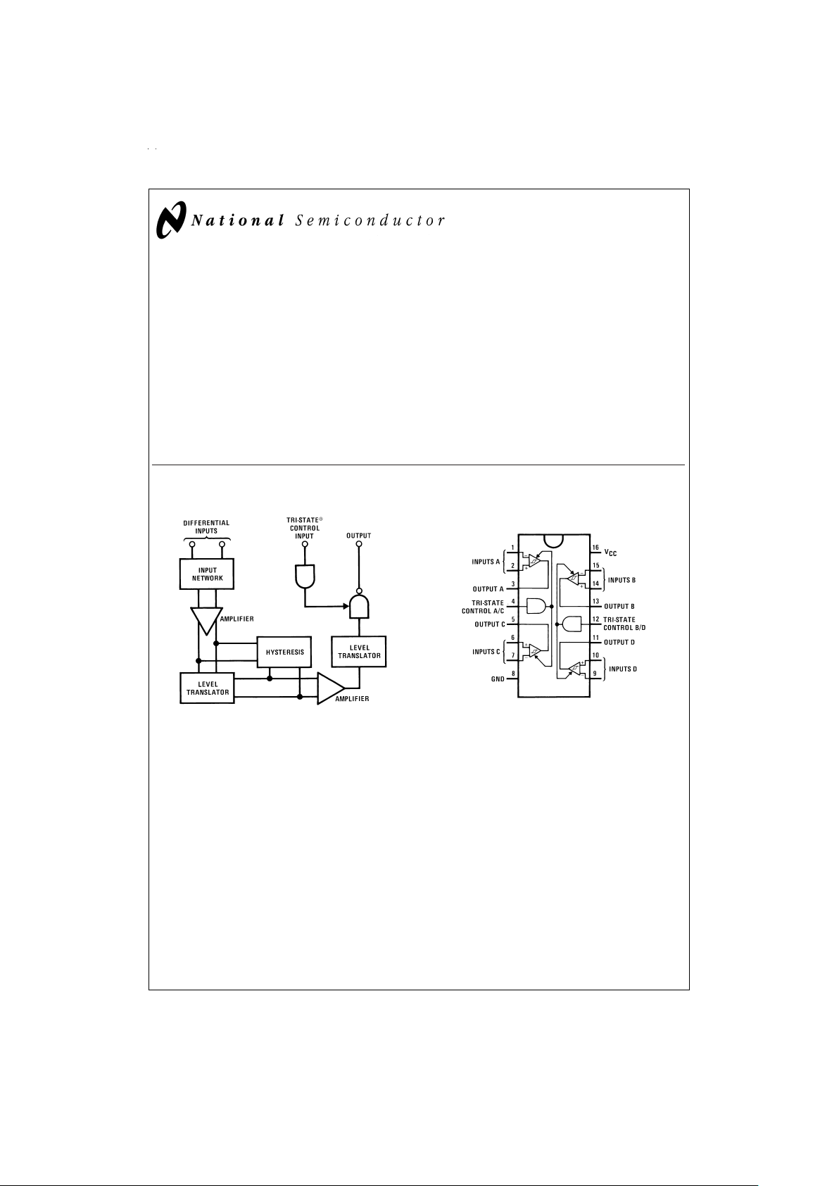
National’s quad RS-422, RS-423 receiver features four independent receivers which comply with EIA Standards for the
electrical characteristics of balanced/unbalanced voltage
digital interface circuits. Receiver outputs are 74LS compatible, TRI-STATE
®
structures which are forced to a high impedance state when the appropriate output control pin
reaches a logic zero condition. A PNP device buffers each
output control pin to assure minimum loading for either logic
one or logic zero inputs. In addition, each receiver has internal hysteresis circuitry to improve noise margin and discourage output instability for slowly changing input waveforms.
Features
n Four independent receivers
n TRI-STATE outputs
n Internal hysteresis −140 mV (typ)
n Fast propagation times −19 ns (typ)
n TTL compatible outputs
n 5V supply
n Pin compatible and interchangeable with MC3486
Block and Connection Diagrams
TRI-STATE®is a registeredtrademark of National Semiconductor Corp.
DS005779-1
Dual-In-Line Package
DS005779-2
Top View
Order Number DS3486M or DS3486N
See NS Package Number M16A or N16E
May 1998
DS3486 Quad RS-422, RS-423 Line Receiver
© 1999 National Semiconductor Corporation DS005779 www.national.com
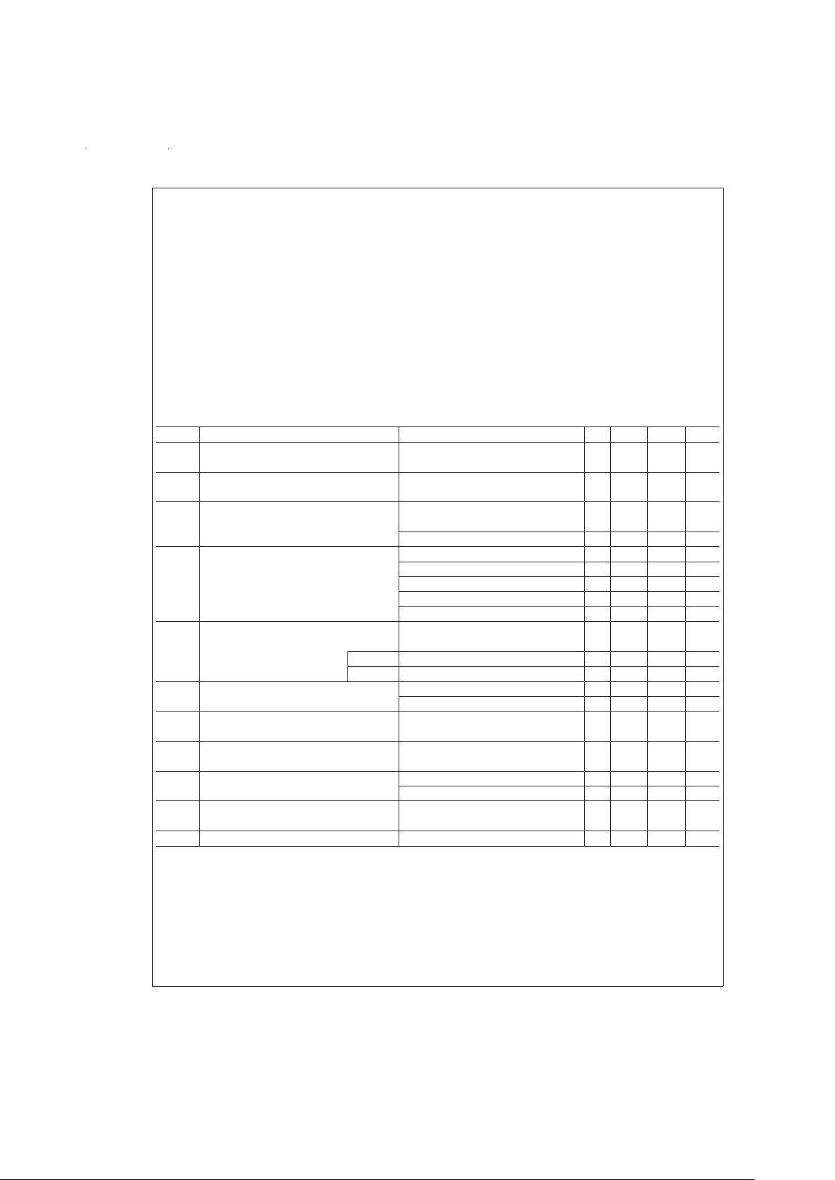
Absolute Maximum Ratings (Note 2)
If Military/Aerospace specified devices are required,
please contact the National Semiconductor Sales Office/
Distributors for availability and specifications.
Power Supply Voltage, V
CC
8V
Input Common-Mode Voltage,
V
ICM
±
25V
Input Differential Voltage, V
ID
±
25V
TRI-STATE Control Input
Voltage, V
I
8V
Output Sink Current, I
O
50 mA
Storage Temperature, T
STG
−65˚C to +150˚C
Maximum Power Dissipation (Note 1) at 25˚C
Molded Dip Package 1362 mW
SO Package 1002 mW
Operating Conditions
Max Min Units
Power Supply Voltage, V
CC
4.75 5.25 V
Operating Temperature, T
A
070˚C
Input Common-Mode Voltage −7.0 7.0 V
Range, V
ICR
Note 1: Derate Dip molded package 10.2 mW/˚C above 25˚C. Derate SO
package 8.01 mW/˚C above 25˚C.
Electrical Characteristics (Note 3)
(Unless otherwise noted, minimum and maximum limits apply over recommended temperature and power supply voltage
ranges. Typical values are for T
A
=
25˚C, V
CC
=
5V and V
IC
=
0V.)
Symbol Parameter Conditions Min Typ Max Units
V
IH
Input Voltage —High Logic State 2.0 V
(TRI-STATE Control)
V
IL
Input Voltage —Low Logic State 0.8 V
(TRI-STATE Control)
V
TH(D)
Differential Input Threshold Voltage −7V ≤ VIC≤ 7V, VIHTRI-STATE=2V 0.070 0.2 V
I
O
=
−0.4 mA, V
OH
≥ 2.7V
I
O
=
8 mA, V
OL
≥ 0.5V 0.070 −0.2 V
I
IB (D)
Input Bias Current V
CC
=
0V or 5.25V, Other Inputs at 0V
V
I
=
−10V −3.25 mA
V
I
=
−3V −1.50 mA
V
I
=
3V 1.50 mA
V
I
=
10V 3.25 mA
Input Balance −7V ≤ V
IC
≤ 7V, V
IH(3C)
=
2V,
(Note 5)
V
OH
I
O
=
−0.4 mA, V
ID
=
0.4V 2.7 V
V
OL
I
O
=
8 mA, V
ID
=
−0.4V 0.5 V
I
OZ
Output TRI-STATE Leakage Current V
I(D)
=
3V, V
IL
=
0.8V, V
OL
=
0.5V −40 µA
V
I(D)
=
−3V, V
IL
=
0.8V, V
OH
=
2.7V 40 µA
I
OS
Output Short-Circuit Current V
I(D)
=
3V, V
IH
TRI-STATE=2V, −15 −100 mA
V
O
=
0V, (Note 4)
I
IL
Input Current —Low Logic State V
IL
=
0.5V −100 µA
(TRI-STATE Control)
I
IH
Input Current —High Logic State V
IH
=
2.7V 20 µA
(TRI-STATE Control) V
IH
=
5.25V 100 µA
V
IC
Input Clamp Diode Voltage I
IN
=
−10 mA −1.5 V
(TRI-STATE Control)
I
CC
Power Supply Current All Inputs V
IL
=
0V 85 mA
Note 2: “Absolute Maximum Ratings” are those values beyond which the safety of the device cannot be guaranteed. They are not meant to imply that the devices
should be operated at these limits. The table of “Electrical Characteristics” provides conditions for actual device operation.
Note 3: All currents into device pins are shown as positive, out of device pins are negative. All voltages referenced to ground unless otherwise noted.
Note 4: Only one output at a time should be shorted.
Note 5: Refer to EIA RS-422/3 for exact conditions.
www.national.com 2
 Loading...