NSC DS32ELX0421SQ, DS32ELX0421 Datasheet

PRELIMINARY
May 9, 2008
DS32EL0421, DS32ELX0421
125 – 312.5 MHz Serializer with DDR LVDS Parallel LVDS
Interface
General Description
The DS32EL0421/DS32ELX0421 is a 125 MHz to 312.5 MHz
(DDR) serializer for high-speed serial transmission over FR-4
printed circuit board backplanes, balanced cables, and optical
fiber. This easy-to-use chipset integrates advanced signal
and clock conditioning functions, with an FPGA friendly interface.
The DS32EL0421/DS32ELX0421 serializes up to 5 parallel
input LVDS channels to create a maximum data payload of
3.125 Gbps. If the integrated DC-balance encoding is enabled, the maximum data payload achievable is 2.5 Gbps.
The DS32EL0421/DS32ELX0421 serializers feature remote
sense capability to automatically detect and negotiate link
status with its companion DS32EL0124/DS32ELX0124 deserializers without requiring an additional feedback path.
The parallel LVDS interface reduces FPGA I/O pins, board
trace count and alleviates EMI issues, when compared to traditional single-ended wide bus interfaces.
The DS32EL0421/DS32ELX0421 is programmable through
a SMBus interface as well as through control pins.
Target Applications
■
Imaging: Industrial, Medical Security, Printers
■
Displays: LED walls, Commercial
■
Video Transport
■
Communication Systems
■
Test and Measurement
■
Industrial Bus
Features
■
5-bit LVDS parallel data interface
■
Programmable transmit de-emphasis
■
Configurable output levels (VOD)
■
Selectable DC-balanced encoder
■
Selectable data scrambler
■
Remote Sense for automatic detection and negotiation of
link status
■
On chip LC VCOs
■
Redundant serial output (ELX device only)
■
Data valid signaling to assist with synchronization of
multiple receivers
■
Supports AC- and DC-coupled signaling
■
Integrated CML and LVDS terminations
■
Configurable PLL loop bandwidth
■
Programmable output termination (50Ω or 75Ω).
■
Built-in test pattern generator
■
Loss of lock and error reporting
■
Configurable via SMBus
■
48-pin LLP package with exposed DAP
Key Specifications
■
1.25 to 3.125 Gbps serial data rate
■
125 to 312.5 MHz DDR parallel clock
■
-40° to +85°C temperature range
■
>8 kV ESD (HBM) protection
■
Low Intrinsic Jitter — 35ps at 3.125 Gbps
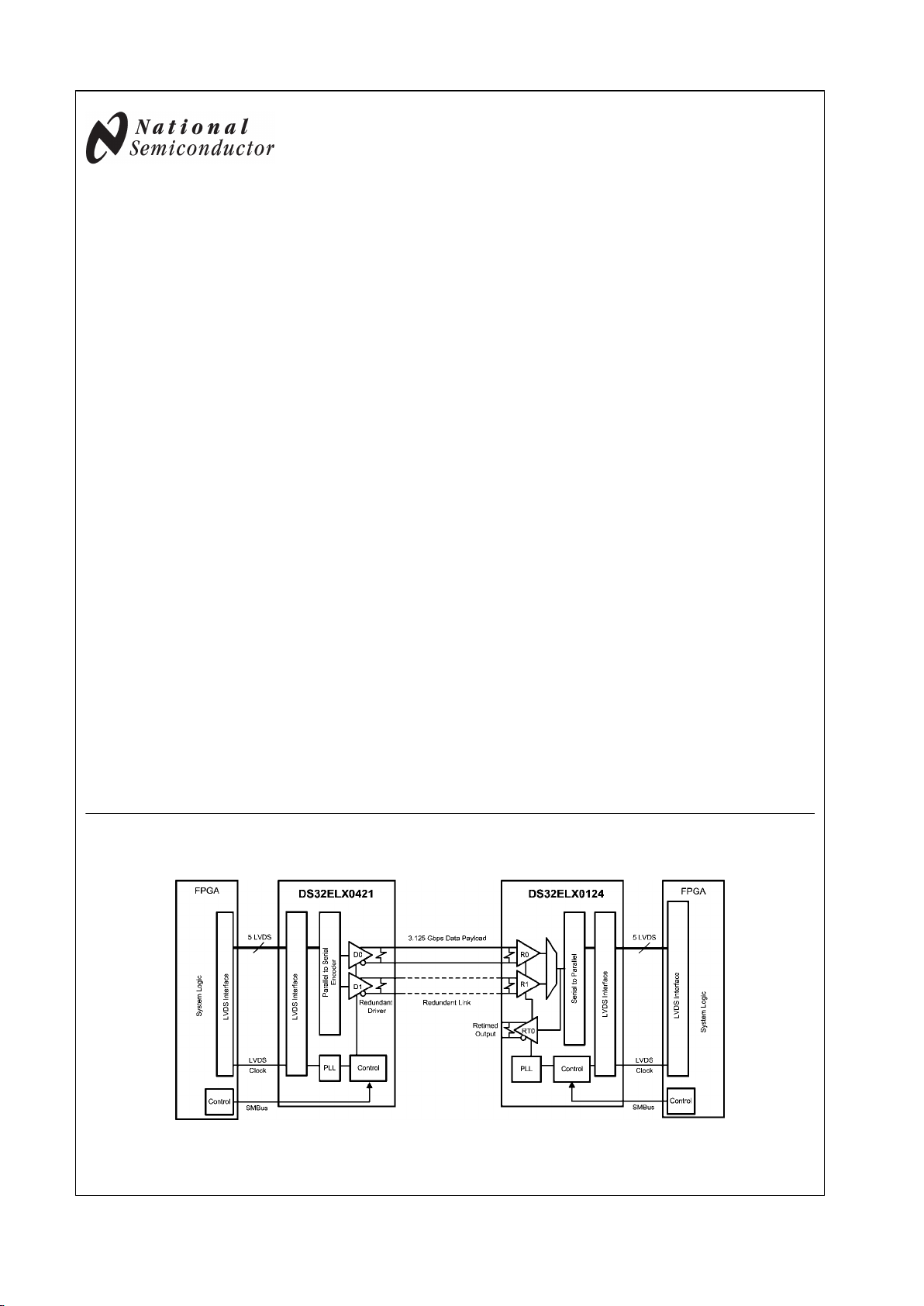
Typical Application
30032101
© 2008 National Semiconductor Corporation 300321 www.national.com
DS32EL0421, DS32ELX0421 125 – 312.5 MHz Serializer with DDR LVDS Parallel LVDS Interface

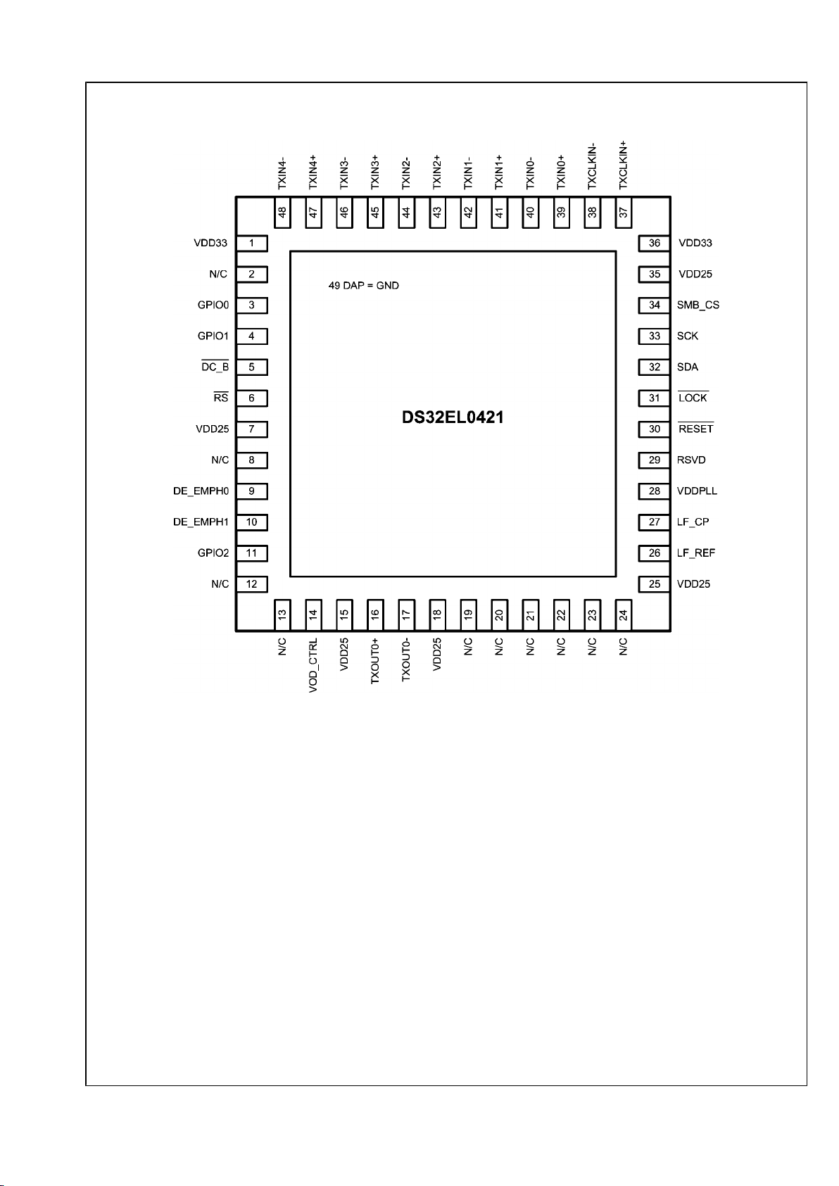
Pin Diagram
30032102
www.national.com 2
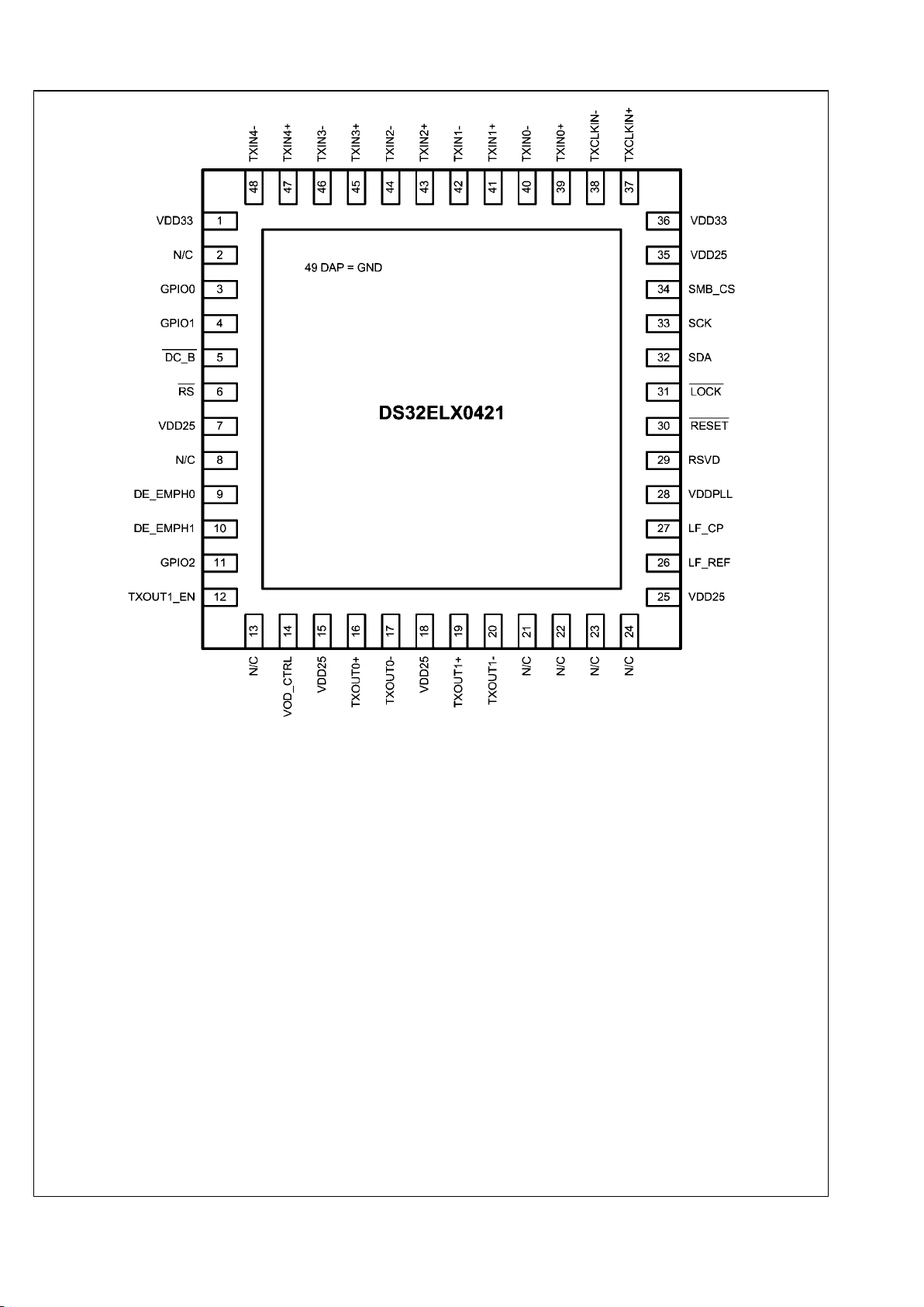
DS32EL0421, DS32ELX0421

30032103
3 www.national.com
DS32EL0421, DS32ELX0421

Pin Descriptions
Pin Name Pin Number I/O, Type Description
Power, Ground and Analog Reference
VDD33 1, 36 I, VDD 3.3V supply
VDD25 7, 15, 18, 25,35I, VDD 2.5V supply
VOD_CTRL 14 Analog VOD control. The serializer output amplitude can be adjusted by connecting this pin to a
pull-down resistor. The value of the resistor determines the VOD. Use the following
equation to determine the value of the resistor.
R = (1400 mV / VOD) x 9.1 kΩ
LF_CP 27 Analog Loop filter connection for PLL
LF_REF 28 Analog Loop filter ground reference
Exposed
Pad
49 GND Exposed Pad must be connected to GND by 9 vias
CML I/O
TxOUT0+
TxOUT0-
16
17
O, CML Inverting and non-inverting high speed CML differential outputs of the serializer. These
outputs are internally terminated.
TxOUT1+
TxOUT1-
19
20
O, CML DS32ELX0421 ONLY. Redundancy output. Inverting and non-inverting high speed CML
differential outputs of the serializer. These outputs are internally terminated
LVDS Parallel Data Bus
TxCLKIN+
TxCLKIN-
37
38
I, LVDS Serializer input clock. TxCLKIN+/- are the inverting and non-inverting LVDS transmit
clock input pins.
TxIN[4:0]+/- 39, 40,
41, 42,
43, 44,
45, 46,
47, 48
I, LVDS Serializer input data. TxIN[4:0]+/- are the inverting and non-inverting LVDS serializer
input data pins.
LVCMOS Control Pins
DC_B
RS
5
6
I,
LVCMOS
DC-balance and Remote Sense pins. See Device Configuration section for device
behavior.
DE_EMPH0
DE_EMPH1
9
10
I,
LVCMOS
DE_EMPH0, DE_EMPH1 select the output de-emphasis level. These pins are internally
pull-down.
00: Off
01: Low
10: Medium
11: Maximum
TXOUT1_E
N
12 I,
LVCMOS
DS32ELX0421 ONLY. When held high, redundant output TxOUT1+/- is enabled.
RESET 30 I,
LVCMOS
When held low, reset the device.
0 = Device Reset
1 = Normal operation
LOCK 31 O,
LVCMOS
Lock indication output. The input data on TxIN[0:4]+/- pins is ignored when LOCK pin is
high.
SMBus Interface
SCK 33 I/O,
SMBus
SMBus compatible clock.
SDA 32 I/O,
SMBus
SMBus compatible data line.
SMB_CS 34 I, SMBus SMBus chip select. When held high, SMBus management control is enabled.
Other
GPIO0 3 I/O,
LVCMOS
Software configurable I/O pin.
www.national.com 4
DS32EL0421, DS32ELX0421

GPIO1 4 I/O,
LVCMOS
Software configurable I/O pin.
GPIO2 11 I/O,
LVCMOS
Software configurable I/O pin.
NC 2, 8, 12, 13,
19, 20, 21,
22, 23, 24,
29
Misc. No Connect, for DS32EL0421
2, 8, 13, 21,
22, 23, 24,
29
Misc. No Connect, for DS32ELX0421
5 www.national.com
DS32EL0421, DS32ELX0421

Absolute Maximum Ratings (Note 1)
If Military/Aerospace specified devices are required,
please contact the National Semiconductor Sales Office/
Distributors for availability and specifications.
Supply Voltage (3.3V VDD)
−0.3V to +4V
Supply Voltage (2.5V VDD)
−0.3V to +3V
LVCMOS Input Voltage −0.3V to (VDD + 0.3V)
LVCMOS Output Voltage −0.3V to (VDD + 0.3V)
LVDS Input Voltage (IN+, IN-) −0.3V to +3.6V
CML Output Voltage −0.3V to +3.6V
Junction Temperature +125°C
Storage Temperature Range -65°C to +150°C
Lead Temperature Range
Soldering (4 sec.) +260°C
Thermal Resistance, θ
JA
25°C/W
ESD Susceptibility
HBM (Note 2) >8 kV
Recommended Operating
Conditions
Min Typ Max Units
Supply Voltage (V
DD33
–
GND)
3.135 3.3 3.465 V
Supply Voltage (V
DD25
–
GND)
2.375 2.5 2.625 V
Supply Noise Amplitude
from 10 Hz to 50 MHz
100 mV
P-P
Ambient Temperature (TA) -40 +25 +85 °C
Power Supply Specifications
Symbol Parameter Condition Min Typ Max Unit
I
DD25
2.5V supply current
1 Output Enabled
1.25 Gbps 87 94
mA
2.5 Gbps 95 105
3.125 Gbps 101 112
2.5V supply current
2 Outputs Enabled
1.25 Gbps 126 135
2.5 Gbps 136 145
3.125 Gbps 142 152
I
DD33
3.3V supply current
1 Output Enabled
1.25 Gbps 74 85
mA
2.5 Gbps 74 85
3.125 Gbps 74 85
3.3V supply current
2 Outputs Enabled
1.25 Gbps 80 92
2.5 Gbps 80 92
3.125 Gbps 80 92
P
D
Power Consumption
1 Output Enabled
1.25 Gbps 460 540
mW
2.5 Gbps 485 560
3.125 Gbps 500 575
Power Consumption
2 Output Enabled
1.25 Gbps 580 670
2.5 Gbps 605 695
3.125 Gbps 620 710
Power Consumption
No clock to TxCLKIN
320
www.national.com 6
DS32EL0421, DS32ELX0421

Electrical and Timing Characteristics
Over recommended operating supply and temperature ranges unless otherwise specified. (Notes 3, 4, 5)
Symbol Parameter Conditions Min Typ Max Units
LVCMOS ELECTRICAL SPECIFICATIONS
V
IH
High Level Input Voltage 2.0 V
DD
V
V
IL
Low Level Input Voltage 0 0.8 V
V
OH
High Level Output Voltage IOH = -2mA 2.7 3.3 V
V
OL
Low Level Output Voltage IOL = 2mA 0.3 V
V
CL
Input Clamp Voltage ICL = -18mA -0.79 -1.5 V
I
IN
Input Current VIN = 0.4V, 2.5V, or V
DD
-35 35
μA
I
OS
Output Short Circuit Current V
OUT
= 0V
(Note 6)
42 mA
SMBus ELECTRICAL SPECIFICATIONS
V
SIL
Data, Clock Input Low Voltage 0.8 V
V
SIH
Data, Clock Input High Voltage 2 V
SDD
V
I
SPULLUP
Current through pull-up resistor or current source 4 mA
V
SDD
Nominal Bus Voltage 2.375 3.6 V
i
SLEAKB
Input Leakage Per Bus Segment ±200
μA
C
SI
capacitance for SDA and SCLK 10 pF
R
STERM
Termination Resistance V
SDD
= 3.3V 1000
Ω
SMBus TIMING SPECIFICATIONS
t
SMB
Bus Operating Frequency 10 100 kHz
t
BUF
Bus Free Time between Stop and Start Condition 4.7
μs
t
HD:STA
Hold time after (repeated) start condition. After this
period, the first clock is generated.
At I
SPULLUP
= MAX 4.0
μs
t
SU:STA
Repeated Start Condition Setup Time 4.7
μs
t
SU:STO
Stop Condition Setup Time 4.0
μs
t
HD:DAT
Data Hold Time 300 ns
t
SU:DAT
Data Setup Time 250 ns
t
LOW
Clock Low Time 4.7
μs
t
HIGH
Clock High Time 4.0 50
μs
t
F
Clock/Data Fall Time 20% to 80% 300 ns
t
R
Clock/Data Rise Time 1000 ns
t
SU:CS
SMB_CS Setup Time 30 ns
t
POR
Time in which the device must be operation after
power on
500 ms
LVDS ELECTRICAL SPECIFICATIONS
V
TH
Differential Input High Threshold
0.05V < V
LVCM
< V
DD25
– 0.05V
+100 mV
V
TL
Differential Input Low Threshold -100 mV
V
LVCM
LVDS Input Common Mode Voltage 0.05 V
DD25
–
0.05
V
V
LVOS
LVDS Input Loss of Signal LVDS input loss of signal level.
(Note 7)
20 mV
P-P
R
LVIN
Input Impedance Internal LVDS input termination
between differential pairs.
85 100 115
Ω
LVDS TIMING SPECIFICATIONS
f Input DDR Clock (TxCLKIN) Frequency Range 125 312.5 MHz
t
CIP
TxCLKIN Period
See Figure 3
3.2 2T 8 ns
7 www.national.com
DS32EL0421, DS32ELX0421

Symbol Parameter Conditions Min Typ Max Units
t
CIT
TxCLKIN Transition Time See Figure 3
(Note 8)
0.5 1.0 3.0 ns
t
XIT
TxIN Transition Time 0.15 3 ns
t
CIH
TxCLKIN High Time See Figure 3 0.7T T 1.3T ns
t
CIL
TxCLKIN Low Time 0.7T T 1.3T ns
t
STC
TxIN Setup to TxCLKIN -550 ps
t
HTC
TxIN Hold to TxCLKIN 900 ps
t
LVDLS
LVDS Input Clock Delay Step Size Programmable through the SMBus,
register 30'h
Default setting = 011'b [7:5]
See Figure 5
100 ps
CML ELECTRICAL SPECIFICATIONS
R
OT
Output Terminations On chip termination from TxOUT0/1
+ and TxOUT0/1 - to V
DD25
50Ω mode
40 50 60
Ω
75Ω mode
60 75 90
Ω
ΔR
OT
Mismatch in Output Termination Resistors 5 %
V
OD
Output Differential Voltage Swing
Based on VOD_CTRL = 9.1 kΩ
1175 1350 1450 mV
P-P
CML TIMING SPECIFICATIONS
LR Line Rate Tested with alternating 1-0 pattern. 1.25 3.125 Gbps
t
OS
Output Overshoot 10 %
t
R
Differential Low to High Transition Time (Note 8) 60 90 ps
t
F
Differential High to Low Transition Time 60 90 ps
t
RFMM
Mismatch in Rise/Fall Time 15 ps
t
DE
De-emphasis width Measured from zero-crossing at
rising edge to 80% of VOD from zerocrossing at falling edge. TDE is
measured at the High setting during
test.
1 UI
t
BIT
Serializer Bit Width 0.2 x
t
CIP
ns
t
SD
Serializer Propagation Delay – Latency t
CIP
+
5.5
ns
t
JIND
Serializer Output Deterministic Jitter Serializer output intrinsic
deterministic jitter. Measure with
PRBS-7 test pattern De-emphasis
disabled.
1.25 Gbps
10
ps
2.5 Gbps 24 ps
3.125 Gbps 21 ps
t
JINR
Serializer Output Random Jitter Serializer output intrinsic random
jitter. Bit error rate ≥10
-15
.
Alternating–10 pattern. De-emphasis
disabled.
1.25 Gbps
1.3
ps
RMS
2.5 Gbps 1.15 ps
RMS
3.125 Gbps 1.14 ps
RMS
www.national.com 8
DS32EL0421, DS32ELX0421
 Loading...