

NSC DS32ELX0124SQ, DS32ELX0124 Datasheet

PRELIMINARY
May 9, 2008
DS32EL0124 DS32ELX0124
125 MHz — 312.5 MHz Deserializer with DDR LVDS Parallel
Interface
DS32EL0124/DS32ELX0124 125 — 312.5 MHz Deserializer with DDR LVDS Parallel Interface
General Description
The DS32EL0124/DS32ELX0124 integrates clock and data
recovery modules for high-speed serial communication over
FR-4 printed circuit board backplanes, balanced cables, and
optical fiber. This easy-to-use chipset integrates advanced
signal and clock conditioning functions, with an FPGA friendly
interface.
The DS32EL0124/DS32ELX0124 deserializes up to 3.125
Gbps of high speed serial data to 5 LVDS outputs without the
need for an external reference clock. With DC-balance decoding enabled, the application payload of 2.5 Gbps is deserialized to 4 LVDS outputs.
The DS32EL0124/DS32ELX01214 deserializers feature a remote sense capability to automatically signal link status conditions to its companion DS32EL0421/ELX0421 serializers
without requiring an additional feedback path.
The parallel LVDS interface of these devices reduce FPGA
I/O pins, board trace count and alleviates EMI issues, when
compared to traditional single-ended wide bus interfaces.
The DS32EL0124/ELX0124 is programmable through a SMBus interface as well as through control pins.
Applications
Imaging: Industrial, Medical Security, Printers
■
Displays: LED walls, Commercial
■
Video Transport
■
Communication Systems
■
Test and Measurement
■
Industrial Bus
■
Features
5-bit LVDS parallel data interface
■
Programmable Receive Equalization
■
Selectable DC-balance decoder
■
Selectable De-scrambler
■
Remote Sense for automatic detection and negotiation of
■
link status
No external receiver reference clock required
■
LVDS parallel interface
■
Programmable LVDS output clock delay
■
Supports output data-valid signaling
■
Supports keep-alive clock output
■
On chip LC VCOs
■
Redundant serial input (ELX device only)
■
Retimed serial output (ELX device only)
■
Configurable PLL loop bandwidth
■
Configurable via SMBus
■
Loss of lock and error reporting
■
48-pin LLP package with exposed DAP
■
Key Specifications
1.25 to 3.125 Gbps serial data rate
■
125 to 312.5 MHz DDR parallel clock
■
-40° to +85°C temperature range
■
> 8 kV ESD (HBM) protection
■
High Jitter Tolerance TBD
■
Low Jitter Transfer TBD
■
Typical Application
30043101
© 2008 National Semiconductor Corporation 300431 www.national.com

Pin Diagrams
DS32EL0124/DS32ELX0124
www.national.com 2
30043102
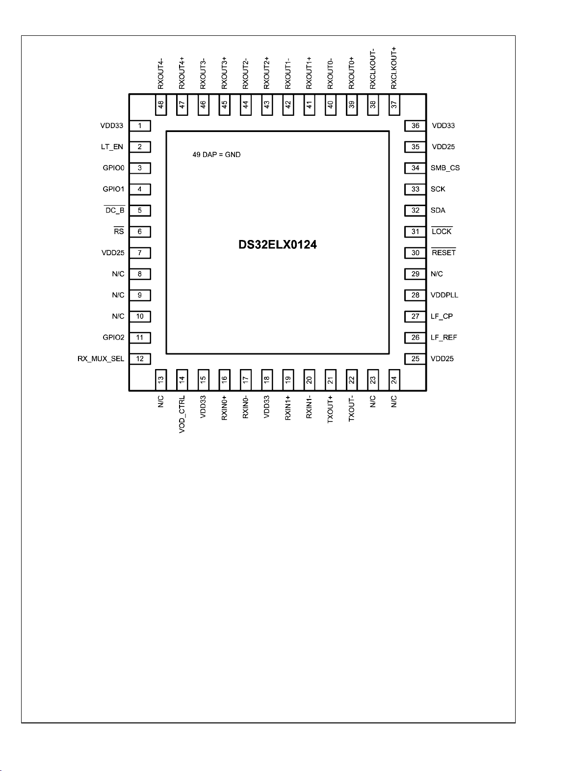
DS32EL0124/DS32ELX0124
30043103
3 www.national.com
Pin Descriptions
Pin Name Pin Number I/O, Type Description
VDD33 1, 15, 18, 35 I, VDD 3.3V supply
VDD25 7, 25, 35 I, VDD 2.5V supply
VDD_PLL 28 I, VDD 3.3V supply
LF_CP 27 Analog Loop filter capacitor connection
LF_REF 26 Analog Loop filter ground reference
Exposed Pad 49 GND Exposed Pad must be connected to GND by 9 vias.
CML I/O
DS32EL0124/DS32ELX0124
RxIN0+
RxIN0-
RxIN1+
RxIN1-
TxOUT+
TxOUT-
LVDS Parallel Data Bus
RxCLKOUT+
RxCLKOUT-3738
RxOUT[0:4]+/- 39, 40, 41, 42, 43, 44, 45,
Control Pins
LT_EN 2 I, LVCMOS DS32ELX0124 only. When held high, retimed serialized high speed
RX_MUX_SEL 12 I, LVCMOS DS32ELX0124 only. RX_MUX_SEL selects the input of the deserializer.
VOD_CTRL 14 I, LVCMOS DS32ELX0124 only. VOD control. The deserializer loop through output
DC_B
RS
RESET 30 I, LVCMOS Reset pin. When held low, reset the device.
LOCK 31 O, LVCMOS Lock indication output. pin goes low when the deserializer is locked to the
SMBus
SCK I, SMBus 33 SMBus compatible clock.
SDA I/O, SMBus 32 SMBus compatible data line.
SMB_CS I, SMBus 34 SMBus chip select. When held high, SMBus management control is
Other
GPIO0 3 I/O, LVCMOS Software configurable IO pins.
GPIO1 4 I/O, LVCMOS Software configurable IO pins.
GPIO2 11 I/O, LVCMOS Software configurable IO pins.
16
17
19
20
21
22
46, 47, 48
5
6
I, CML Non-inverting and inverting high speed CML differential inputs of the
deserializer. These inputs are internally terminated.
I, CML DS32ELX0124 only. Non-inverting and inverting high speed CML
differential inputs of the deserializer. These inputs are internally
terminated.
O, CML DS32ELX0124 only. Retimed serialized high speed output. Non-inverting
and inverting speed CML differential outputs of the deserializer. These
outputs are internally terminated.
O, LVDS Deserializer output clock. RxCLKOUT+/- are the non-inverting and
inverting LVDS recovered clock output pins.
O, LVDS Deserializer output data. RxOUT[0:4]+/- are the non-inverting and
inverting LVDS deserialized output data pins.
output is enabled.
0 = RxIN0+/- selected
1 = RxIN1+/- selected
amplitude can be adjusted by connecting this pin to a pull-down resistor.
The value of the pull-down resistor determines the VOD. Use the following
equation to determine the value of the pull-down resistor.
I, LVCMOS DC-balance and Remote Sense pins. See Application section for device
behavior.
0 = Device Reset
1 = Normal operation
incoming data stream and begins to output data and clock on RxOUT and
RxCLKOUT respectively.
0 = Deserializer locked
1 = Deserializer not locked
enabled.
www.national.com 4

DS32EL0124/DS32ELX0124
NC
2 ,8, 9, 10, 12, 13, 14, 19,
20, 21, 22, 23, 24, 29
8, 9, 10, 13, 23, 24, 29 Misc No Connect, for DS32ELX0124
Misc. No Connect, for DS32EL0124
5 www.national.com

Absolute Maximum Ratings (Note 1)
If Military/Aerospace specified devices are required,
please contact the National Semiconductor Sales Office/
Distributors for availability and specifications.
Supply Voltage (V
Supply Voltage (V
LVCMOS Input Voltage −0.3V to (V
LVCMOS Output Voltage -0.3V to (V
CML Input/Output Voltage -0.3V to 3.6V
LVDS Output Voltage -0.3V to +3.6V
DS32EL0124/DS32ELX0124
Junction Temperature +125°C
Storage Temperature Range −65°C to +150°C
Lead Temperature Range
Soldering (4 sec.) +260°C
Package Thermal Resistance
θ
JA
ESD Susceptibility
HBM
DD33
DD25
)
)
−0.3V to +4V
-0.3V to +3.0V
DD33
DD33
+ 0.3V)
+ 0.3V)
+25.0°C/W
≥8 kV
Recommended Operating Conditions
Min Typ Max Units
Supply Voltage (V
Supply Voltage (V
Supply Noise Amplitude
from 10 Hz to 50 MHz
Ambient Temperature (TA) −40 +25 +85 °C
) 3.135 3.3 3.485 V
DD33
) 2.375 2.5 2.625 V
DD25
100 mV
Electrical and Timing Characteristics
Over recommended operating supply and temperature ranges unless otherwise specified. (Notes 2, 3, 4)
Symbol Parameter Conditions Min Typ Max Units
LVCMOS ELECTRICAL SPECIFICATIONS
V
IH
V
IL
V
OH
V
OL
V
CL
I
IN
I
OS
SMBus ELECTRICAL SPECIFICATIONS
V
SIL
V
SIH
I
SPULLUP
V
SDD
I
SLEAKB
I
SLEAKP
C
SI
R
STERM
SMBus TIMING SPECIFICATIONS
f
SMB
t
BUF
t
HD:STA
t
SU:STA
t
HD:DAT
t
SU:DAT
t
LOW
t
HIGH
High Level Input Voltage 2.0 V
DD
Low Level Input Voltage GND 0.8 V
High Level Output Voltage IOH = -2mA 2.7 3.3 V
Low Level Output Voltage IOL = 2mA 0.3V V
Input Clamp Voltage ICL = −18 mA -0.9 −1.5 V
Input Current VIN = 0.4V, 2.5V, or V
Output Short Circuit Current V
OUT
= 0V
DD33
-35 1 35
TBD V
(Note 5)
Data, Clock Input Low Voltage 0.8 V
Data, Clock Input High Voltage 2.1 V
SDD
Current through pull-up resistor or current source 4 mA
Nominal Bus Voltage 2.375 3.6 V
Input Leakage Per Bus Segment ±200 µA
Input Leakage Per Pin ±10 µA
Capacitance for SDA and SCK 10 pF
SMBus Termination Resistor Value V
= 3.3V 1000
SDD
Bus Operating Frequency 10 100 kHz
Bus free time between top and start condition 4.7
Hold time after (repeated) start condition. After this
At I
= MAX 4.0 µs
SPULLUP
period, the first clock is generated
Repeated Start Condition Setup Time 4.7 µs
Data Hold Time 300 ns
Data Setup Time 250 ns
Clock Low Time 4.7 µs
Clock High Time 4.0 50 µs
P-P
V
μA
V
Ω
μs
www.national.com 6
Symbol Parameter Conditions Min Typ Max Units
t
F
t
R
t
SU:CS
t
POR
Clock/Data Rise Time 20% to 80% 300 ns
Clock/Data Rise Time 1000 ns
SMB_CS Setup Time 30 ns
Time in which the device must be operational after
500 ms
power on
LVDS ELECTRICAL SPECIFICATIONS
R
I
OS
V
ΔV
V
ΔV
I
OS
OUT
OD
OS
Output Termination Resistor Between OUT+ and OUT- 85 100 115
Output Short Circuit Current
Differential Output Voltage
V
= 0V, RL = 100Ω
OUT
RL = 100Ω
Changes in VOD between complimentary output
OD
states
Offset Voltage
Change in VOS between complimentary states 35 mV
OS
Output Short Circuit Current
V
= 0V, RL = 100Ω
OUT
TBD
230 310 mV
35 mV
1.125 1.25 1.375 V
50 mA
Ω
LVDS TIMING SPECIFICATIONS
t
ROTR
t
ROTF
t
ROCP
t
RODC
t
RBIT
t
ROSC
t
ROHC
t
ROJD
t
ROJR
t
ROJT
t
RD
t
RPLLS
t
RLAPL
t
RLA
t
LVSK
LVDS low-to-high transition time 300 ps
LVDS high-to-low transition time 300 ps
LVDS output clock period 2T ns
RxCLKOUT Duty Cycle 45 50 55 %
LVDS output bit width TBD
RxOUT Setup to RxCLKOUT OUT 200 ps
RxOUT Hold to RxCLKOUT OUT 200 ps
LVDS Output Deterministic Jitter TBD
LVDS Output Random Jitter 2.5 ps
Peak-to-Peak LVDS Output Jitter TBD
Deserializer propagation delay – Latency TBD
Deserializer phase lock loop set
TBD
Deserializer Link Acquisition After PLL Lock. TBD
Deserializer Lock Time TBD
LVDS Output Skew LVDS Differential Output Skew
20 ps
between + and - pins
CML INPUT TIMING SPECIFICATIONS
EQDJ Residual deterministic jitter at EQ Output TBD
TOL
Serial Input Jitter Tolerance TBD
JIT
CML INPUT ELECTRICAL SPECIFICATIONS
V
V
I
IN
R
ΔR
ID
IN
IT
Differential input voltage TBD
Single ended input voltage TBD
Input Current TBD
Input Termination TBD
Mismatch in input terminations TBD
IT
CML RETIMED LOOP THROUGH OUTPUT ELECTRICAL SPECIFICATIONS, DS32ELX0124 ONLY
V
R
ΔR
LTOD
LTOT
Output differential voltage TBD
Output termination TBD
Mismatch in output termination resistors TBD
LTOT
CML RETIMED LOOP THROUGH OUTPUT TIMING SPECIFICATIONS, DS32ELX0124 ONLY
t
JIT
t
OS
Additive Output Jitter TBD
Output Overshoot TBD
DS32EL0124/DS32ELX0124
7 www.national.com

Symbol Parameter Conditions Min Typ Max Units
t
LTR
Retimed output driver differential low to high
TBD
transition time
t
LTF
Retimed output driver differential high to low
TBD
transition time
t
LTRFMM
t
LTDE
DS32EL0124/DS32ELX0124
Mismatch in Rise/Fall Time TBD
Retimed driver de-emphasis width TBD
Note 1: “Absolute Maximum Ratings” indicate limits beyond which damage to the device may occur, including inoperability and degradation of device reliability
and/or performance. Functional operation of the device and/or non-degradation at the Absolute Maximum Ratings or other conditions beyond those indicated in
the Recommended Operating Conditions is not implied. The Recommended Operating Conditions indicate conditions at which the device is functional and the
device should not be operated beyond such conditions.
Note 2: The Electrical and Timing Characteristics tables list guaranteed specifications under the listed Recommended Operating Conditions except as otherwise
modified or specified by the Electrical Characteristics Conditions and/or Notes. Typical specifications are estimations only and are not guaranteed.
Note 3: Current into device pins is defined as positive. Current out of device pins is defined as negative. All voltages are referenced to ground except VOD and
ΔVOD.
Note 4: Typical values represent most likely parametric norms for VCC = +3.3V and TA = +25°C, and at the Recommended Operation Conditions at the time of
product characterization and are not guaranteed.
Note 5: Output short circuit current (IOS) is specified as magnitude only, minus sign indicates direction only.
Note 6: Tested with a combination of the 1100000101 (K28.5+ character) and 0011111010 (K28.5- character) patterns. Input stimulus jitter is subtracted
algebraically.
www.national.com 8
 Loading...