

DS1487
Low Power RS-485
1
⁄4Unit Load Multipoint Transceiver
General Description
The DS1487 is a low-power transceiver for RS-485 and
RS-422 communication. The device contains one driver and
one receiver.The drivers slew rate allows for operation up to
2.0 Mbps (see Applications Information section). The transceiver presents
1
⁄4unit loading to the RS-485 bus allowing up
to 128 nodes to be connected together without the use of repeaters.
The transceiver draws 200 µA of supply current when unloaded or fully loaded with the driver disabled and operates
from a single +5V supply.
The driver is short-circuit current limited and is protected
against excessive power dissipation by thermal shutdown
circuitry that places the driver outputs into TRI-STATE
®
(High Impedance state) under fault conditions. The driver
guarantees a minimum of 1.5V differential output voltage
with maximum loading across the common mode range
(V
OD3
).
The receiver has a failsafe feature that guarantees a
logic-high output if the input is open circuit.
The DS1487 is available in surface mount and DIP packages.
Features
n Meets TIA/EIA RS-485 multipoint standard
n Allows up to 128 transceivers on the bus (
1
⁄4U.L.)
n Guaranteed full load output voltage (V
OD3
)
n Low quiescent current: 200 µA typ
n −7V to +12V common-mode input voltage range
n TRI-STATE outputs on driver and receiver
n AC performance:
— Driver transition time: 25 ns typ
— Driver propagation delay: 40 ns typ
— Driver skew: 1 ns typ
— Receiver propagation delay: 200 ns typ
— Receiver skew: 20 ns typ
n Half-duplex flow through pinout
n Operates from a single 5V supply
n Current-limiting and thermal shutdown for driver
overload protection
n Pin and functional compatible with MAX1487
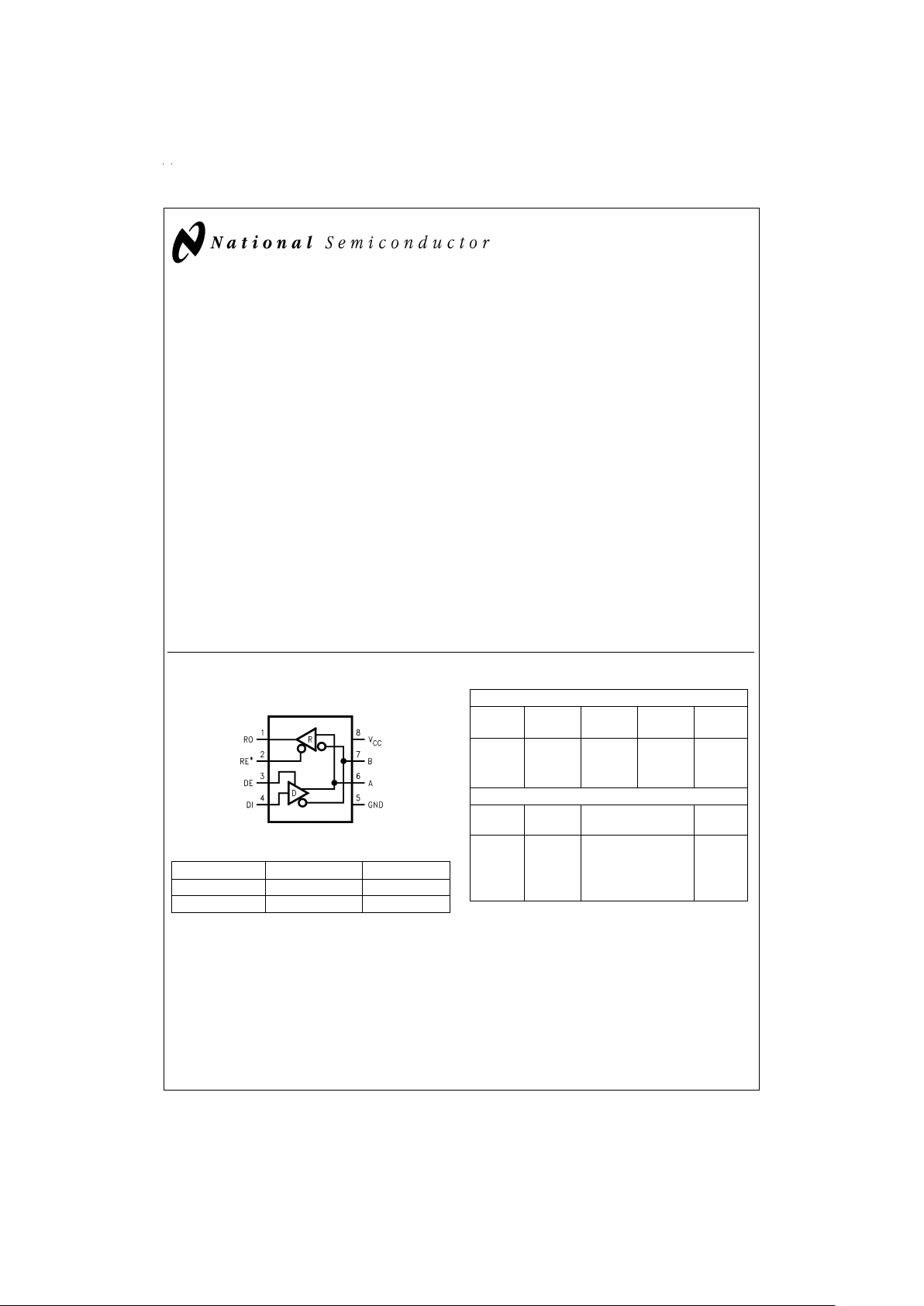
Connection and Logic Diagram
Order Number Temp. Range Package/
###
DS1487N 0˚C to +70˚C DIP/N08E
DS1487M 0˚C to +70˚C SOP/M08A
Truth Table
DRIVER SECTION
RE
(Note 1)
DE DI A B
XHHHL
XHLLH
XLXZZ
RECEIVER SECTION
RE
(Note 1)
DE A-B RO
LL ≥+0.2V H
LL ≤−0.2V L
HX X Z
L L OPEN (Note 1) H
X=indeterminate
Z=TRI-STATE
Note 1: Non Terminated, Open Input only
TRI-STATE®is a registered trademark of National Semiconductor Corporation.
DIP and SOIC
DS012920-1
*Note: Non Terminated, Open Input only
July 1998
DS1487 Low Power RS-485
1
⁄
4
Unit Load Multipoint Transceiver
© 1999 National Semiconductor Corporation DS012920 www.national.com
Absolute Maximum Ratings (Note 2)
If Military/Aerospace specified devices are required,
please contact the National Semiconductor Sales Office/
Distributors for availability and specifications.
Supply Voltage (V
CC
) +12V
Enable Input Voltage
(RE (Note 1), DE) −0.5V to (V
CC
+ 0.5V)
Driver Input Voltage (DI) −0.5V to (V
CC
+ 0.5V)
Driver Output Voltage (A, B) −14V to +14V
Receiver Input Voltage (A, B) −14V to +14V
Receiver Output Voltage (RO) −0.5V to (V
CC
+ 0.5V)
Maximum Package Power Dissipation
@
+25˚C
M Package 1.19W
N Package 0.74W
Derate M Package 9.5 mW/˚C above +25˚C
Derate N Package 6.0 mW/˚C above +25˚C
Maximum Package Power Dissipation
@
+70˚C
M Package 0.76W
N Package 0.47W
Storage Temperature Range −65˚C to +150˚C
Lead Temperature Range
(Soldering, 4 sec.) +260˚C
ESD (HBM) ≥2kV
Recommended Operating
Conditions
Min Typ Max Units
Supply Voltage (V
CC
) +4.75 +5.0 +5.25 V
Operating Free Air
Temperature (T
A
)
DS1487 0 +25 +70 ˚C
Bus Common Mode Voltage −7 +12 V
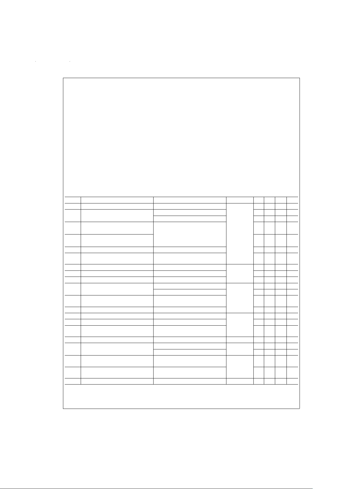
Electrical Characteristics
Over Supply Voltage and Operating Temperature Ranges, unless otherwise specified (Notes 3, 4)
Symbol Parameter Conditions Pin Min Typ Max Units
V
OD1
Differential Driver Output Voltage (No Load) A, B 1.5 5 V
V
OD2
Differential Driver Output Voltage R
L
=
50Ω, (RS422),
Figure 1
2 2.8 V
with Load R
L
=
27Ω, (RS485),
Figure 1
1.5 2.3 5 V
∆V
OD
Change in Magnitude of Output R
L
=
27Ω or 50Ω (Note 5) 0.2 |V|
Differential Voltage
V
OD3
Differential Driver Output Voltage— R1=54Ω,R2=375Ω 1.5 2.0 5 V
Full Load with Max V
CM
V
TEST
=
−7V to +12V,
Figure 2
V
OC
Driver Common-Mode Output Voltage R
L
=
27Ω or 50Ω,
Figure 1
03V
∆V
OC
Change in Magnitude of
Common-Mode Output Voltage
R
L
=
27Ω or 50Ω,
Figure 1
(Note 5)
0.2 |V|
V
IH
Input High Voltage DI, DE, 2.0 V
V
IL
Input Low Voltage RE (Note 1) 0.8 V
I
IN1
Input Current V
IN
=
0V or V
CC
±
2µA
I
IN2
Input Current (Note 6) V
IN
=
+12V A, B 0 190 250 µA
DE=0V, V
CC
=
0V or 5.25V V
IN
=
−7V 0 −100 −200 µA
V
TH
Receiver Differential Threshold
Voltage
−7V ≤ VCM≤ +12V −0.2 0.2 V
∆V
TH
Receiver Input Hysteresis V
CM
=
0V 70 mV
V
OH
Receiver Output High Voltage I
O
=
−4 mA, V
ID
=
0.2V RO 3.5 V
V
OL
Receiver Output Low Voltage I
O
=
4 mA, V
ID
=
−0.2V 0.5 V
I
OZR
TRI-STATE Output Current at
Receiver
0.4V ≤ VO≤ 2.4V
±
1µA
R
IN
Receiver Input Resistance −7V ≤ VIN≤ +12V A, B 48 68 kΩ
I
CC
No-Load Supply Current (Note 7) DE=VCC, RE (Note 1)=0V or V
CC
V
CC
200 500 µA
DE=0V, RE (Note 1)=0V or V
CC
200 500 µA
I
OSD1
Driver Short Circuit Current, V
O
=
HIGH
−7V ≤ V
O
≤ +12V A, B 250 mA
I
OSD2
Driver Short Circuit Current, V
O
=
LOW
−7V ≤ V
O
≤ +12V −250 mA
I
OSR
Receiver Short Circuit Current V
O
=
GND RO 7 85 mA
www.national.com 2
Switching Characteristics
Over Supply Voltage and Operating Temperature Ranges, unless otherwise specified (Notes 4, 8, 9)
Symbol Parameter Conditions Min Typ Max Units
t
PLHD
Driver Differential Propagation Delay— Low to High R
L
=
54Ω,C
L
=
100 pF 10 40 80 ns
t
PHLD
Driver Differential Propagation Delay— High to Low 10 39 80 ns
t
SKEW
Differential Skew |t
PHLD−tPLHD
|0110ns
t
r
Driver Rise Time 32550 ns
t
f
Driver Fall Time 32550 ns
t
ZH
Driver Enable to Output High C
L
=
100 pF 50 200 ns
t
ZL
Driver Enable to Output Low C
L
=
100 pF 65 200 ns
t
LZ
Driver Disable from Output Low C
L
=
15 pF 80 200 ns
t
HZ
Driver Disable from Output High C
L
=
15 pF 80 200 ns
t
PLHD
Receiver Differential Propagation Delay— Low to High C
L
=
15 pF (RO) 30 190 400 ns
t
PHLD
Receiver Differential Propagation Delay— High to Low 30 210 400 ns
t
SKEW
Differential Skew |t
PHLD−tPLHD
| 0 20 50 ns
t
ZH
Receiver Enable to Output High C
L
=
15 pF 45 150 ns
t
ZL
Receiver Enable to Output Low 40 150 ns
t
LZ
Receiver Disable from Output Low 50 150 ns
t
HZ
Receiver Disable from Output High 55 150 ns
f
max
Maximum Data Rate (Note 10) 2.0 Mbps
Note 2: “Absolute Maximum Ratings” are those values beyond which the safety of the device cannot be guaranteed. They are not meant to imply that the devices
should be operated at these limits. The table of “Electrical Characteristics” specifies conditions of device operation.
Note 3: Current into device pins is defined as positive. Current out of device pins is defined as negative. All voltages are referenced to ground except V
OD1/2/3
and
V
ID
.
Note 4: All typicals are given for: V
CC
=
+5.0V, T
A
=
+25˚C.
Note 5: ∆|V
OD
| and ∆|VOC| are changes in magnitude of VODand VOCrespectively, that occur when the input changes state.
Note 6: I
IN2
includes the receiver input current and driver TRI-STATE leakage current.
Note 7: Supply current specification is valid for loaded transmitters when DE=0V or enabled (DE=H) with no load.
Note 8: f=1 MHz, t
r
and tf≤ 6 ns, Z
O
=
50Ω.
Note 9: C
L
includes jig and probe capacitance.
Note 10: f
max
is the guaranteed data rate for 50 ft of twisted pair cable. f
max
may be conservatively determined from the ratio of driver transition time (tr) to the data
rate unit interval (1/f
max
). Using a 10%ratio yields f
max
=
(0.1)/50 ns=2.0 Mb/s. Higher data rates may be supported by allowing larger ratios.
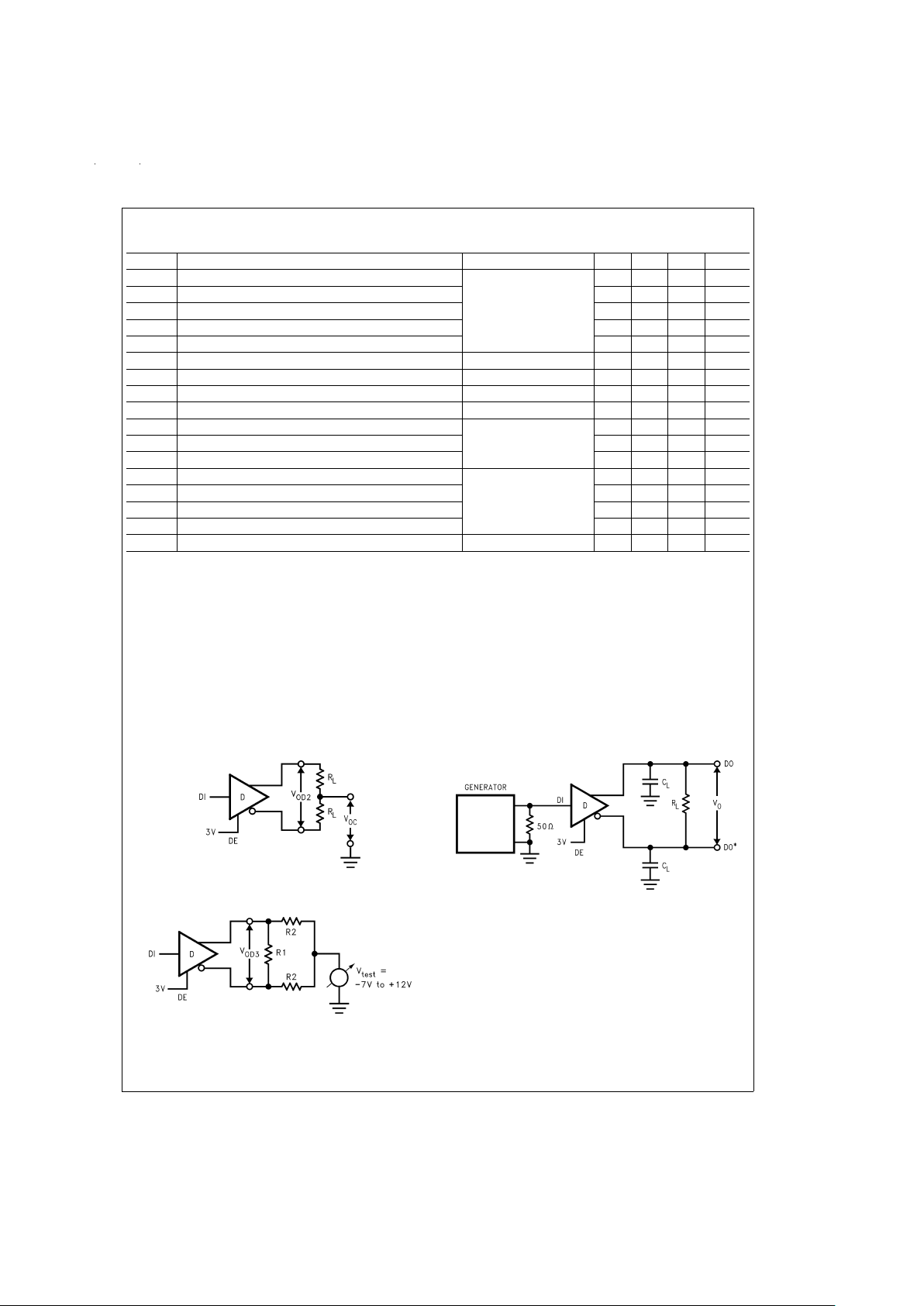
Parameter Measurement Information
DS012920-2
FIGURE 1. V
OD
DS012920-3
FIGURE 2. V
OD3
DS012920-4
FIGURE 3.
www.national.com3

Parameter Measurement
Information
(Continued)
DS012920-5
FIGURE 4.
DS012920-6
FIGURE 5.
DS012920-7
FIGURE 6.
DS012920-8
FIGURE 7.
DS012920-9
FIGURE 8.
DS012920-10
*Note: Non Terminated, Open Input only
FIGURE 9.
DS012920-11
FIGURE 10.
DS012920-12
*Note: Non Terminated, Open Input only
FIGURE 11.
www.national.com 4

Parameter Measurement Information (Continued)
Pin Descriptions
Pin#I/O Name Function
1 O RO Receiver Output: If A
>
B by 200 mV, RO will be high; If A<B by 200 mV, RO will be low. RO will
be high also if the inputs (A and B) are open (non-terminated).
2 I RE (Note 1) Receiver Output Enable: RO is enabled when RE (Note 1) is low; RO is in TRI-STATE when RE
(Note 1) is high.
3 I DE Driver Output Enable: The driver outputs (A and B) are enabled when DE is high; they are in
TRI-STATE when DE is low. Pins A and B also function as the receiver input pins (see below).
4 I DI Driver Input: A low on DI forces A low and B high while a high on DI forces A high and B low when
the driver is enabled.
5 NA GND Ground
6 I/O A Non-inverting Driver Output and Receiver Input pin. Driver output levels conform to RS-485 signaling
levels.
7 I/O B Inverting Driver Output and Receiver Input pin. Driver output levels conform to RS-485 signaling
levels.
8NA V
CC
Power Supply: 4.75V ≤ VCC≤ 5.25V
Applications Information
The DS1487 is a low power transceiver designed for use in
RS-485 multipoint applications. The DS1487 can transmit
data up to 2.0 Mbps based on a ratio of driver transition time
to the unit interval (bit time) of 10%. This maximum data rate
may be further limited by the interconnecting media. The
DS1487 provides a
1
⁄4unit load to the RS-485 bus across the
common mode range of −7V to +12V.This allows up to 128
transceivers (
1
⁄4unit load) to be connected to the bus. The
DS1487 also guarantees the driver’s output differential voltage into a worst case load that models standard termination
loads and 32 unit loads (=128 DS1487’s) referenced to the
maximum common mode voltage extremes. With a minimum
of 1.5V swing into this load, a 1.3V differential noise margin
is supported along with the standard common mode rejection range of the receivers.
DS012920-13
*Note: Non Terminated, Open Input only
FIGURE 12.
DS012920-14
*Note: Non Terminated, Open Input only
FIGURE 13.
www.national.com5

Applications Information (Continued)
Due to the multipoint nature of the bus, contention between
drivers may occur.This will not cause damage to the drivers
since they feature short-circuit protection and also thermal
shutdown protection. Thermal shutdown senses die temperature and puts the driver outputs into TRI-STATE if a fault
condition occurs that causes excessive power dissipation
which can elevate the junction temperature to +150˚C.
A typical multipoint application is shown in the following figure. Note that termination is typically required but is only located at the two ends of the cable (not on every node). Commonly pull up and pull down resistors may be required at one
end of the bus to provide a failsafe bias. These resistors provide a bias to the line when all drivers are in TRI-STATE.See
National Application Note 847 for a complete discussion of
failsafe biasing of differention buses.
DS012920-16
www.national.com 6

Physical Dimensions inches (millimeters) unless otherwise noted
Order Number DS1487N
NS Package Number N08E
www.national.com7

LIFE SUPPORT POLICY
NATIONAL’S PRODUCTS ARE NOT AUTHORIZED FOR USE AS CRITICAL COMPONENTS IN LIFE SUPPORT DEVICES OR SYSTEMS WITHOUT THE EXPRESS WRITTEN APPROVAL OF THE PRESIDENT OF NATIONAL SEMICONDUCTOR CORPORATION. As used herein:
1. Life support devices or systems are devices or systems which, (a) are intended for surgical implant into
the body, or (b) support or sustain life, and whose failure to perform when properly used in accordance
with instructions for use provided in the labeling, can
be reasonably expected to result in a significant injury
to the user.
2. A critical component is any component of a life support
device or system whose failure to perform can be reasonably expected to cause the failure of the life support
device or system, or to affect its safety or effectiveness.
National Semiconductor
Corporation
Americas
Tel: 1-800-272-9959
Fax: 1-800-737-7018
Email: support@nsc.com
www.national.com
National Semiconductor
Europe
Fax: +49 (0) 1 80-530 85 86
Email: europe.support@nsc.com
Deutsch Tel: +49 (0) 1 80-530 85 85
English Tel: +49 (0) 1 80-532 78 32
Français Tel: +49 (0) 1 80-532 93 58
Italiano Tel: +49 (0) 1 80-534 16 80
National Semiconductor
Asia Pacific Customer
Response Group
Tel: 65-2544466
Fax: 65-2504466
Email: sea.support@nsc.com
National Semiconductor
Japan Ltd.
Tel: 81-3-5639-7560
Fax: 81-3-5639-7507
DS1487 Low Power RS-485
1
⁄
4
Unit Load Multipoint Transceiver
National does not assume any responsibility for use of any circuitry described, no circuit patent licenses are implied and National reserves the right at any time without notice to change said circuitry and specifications.
 Loading...