NSC DP83902AV, DP83902AVLJ, DP83902AVJG Datasheet
PRELIMINARY
November 1995
DP83902A ST-NIC Serial Network Interface Controller for Twisted Pair
DP83902A ST-NIC
TM
Serial Network Interface Controller for Twisted Pair
General Description
The DP83902A Serial Network Interface Controller for
Twisted Pair (ST-NIC) is a microCMOS VLSI device designed for easy implementation of CSMA/CD local area networks. These include Ethernet (10BASE5), Thin Ethernet
(10BASE2) and Twisted-pair Ethernet (10BASE-T). The
overall ST-NIC solution provides the Media Access Control
(MAC) and Encode-Decode (ENDEC) with an AUI interface,
and 10BASE-T transceiver functions in accordance with the
IEEE 802.3 standards.
The DP83902A’s 10BASE-T transceiver fully complies with
the IEEE standard. This functional block incorporates the
receiver, transmitter, collision, heartbeat, loopback, jabber,
and link integrity blocks as defined in the standard. The
transceiver when combined with equalization resistors,
transmit/receive filters, and pulse transformers provides a
complete physical interface from the DP83902A’s ENDEC
module and the twisted pair medium.
The integrated ENDEC module allows Manchester encoding and decoding via a differential transceiver and phase
lock loop decoder at 10 Mbit/sec. Also included are collision detect translator and diagnostic loopback capability.
The ENDEC module interfaces directly to the transceiver
module, and also provides a fully IEEE compliant AUI (Attachment Unit Interface) for connection to other media
transceivers. (Continued)
Features
Y
Single chip solution for IEEE 802.3, 10BASE-T
Y
Integrated controller, ENDEC, and transceiver
Y
Full AUI interface
Y
No external precision components required
Y
3 levels of loopback supported
Transceiver Module
Y
Integrates transceiver electronics, including:
Ð Transmitter and receiver
Ð Collision detect, heartbeat and jabber timer
Ð Link integrity test
Y
Link disable and polarity detection/correction
Y
Integrated smart receive squelch
Y
Reduced squelch level for extended distance cable operation (100-pin QFP version)
ENDEC Module
Y
10 Mb/s Manchester encoding/decoding, plus clock recovery
Y
Transmitter half or full step mode
Y
Squelch on receive and collision pairs
Y
Lock time 5 bits typical
Y
Decodes Manchester data with up tog18 ns jitter
MAC/Controller Module
Y
100% DP8390 software/hardware compatible
Y
Dual 16-bit DMA channels
Y
16-byte internal FIFO
Y
Efficient buffer management implementation
Y
Independent system and network clocks
Y
Supports physical, multicast and broadcast address filtering
Y
Network statistics storage
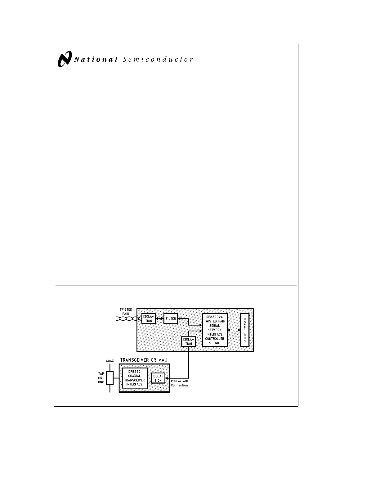
1.0 System Diagram
Station or DTE
TRI-STATEÉis a registered trademark of National Semiconductor Corporation.
TM
ST-NIC
is a trademark of National Semiconductor Corporation.
C
1995 National Semiconductor Corporation RRD-B30M115/Printed in U. S. A.
TL/F/11157
TL/F/11157– 1
General Description (Continued)
The Media Access Control function which is provided by the
Network Interface Control module (NIC) provides simple
and efficient packet transmission and reception control by
means of unique dual DMA channels and an internal FIFO.
Bus arbitration and memory control logic are integrated to
reduce board cost and area overheads.
DP83902A provides a comprehensive single chip solution
for 10BASE-T IEEE 802.3 networks and is designed for
easy interface to other transceivers via the AUI interface.
Due to the inherent constraints of CMOS processing, isolation is required at the AUI differential signal interface for
10BASE5 and 10BASE2 applications. Capacitive or inductive isolation may be used.
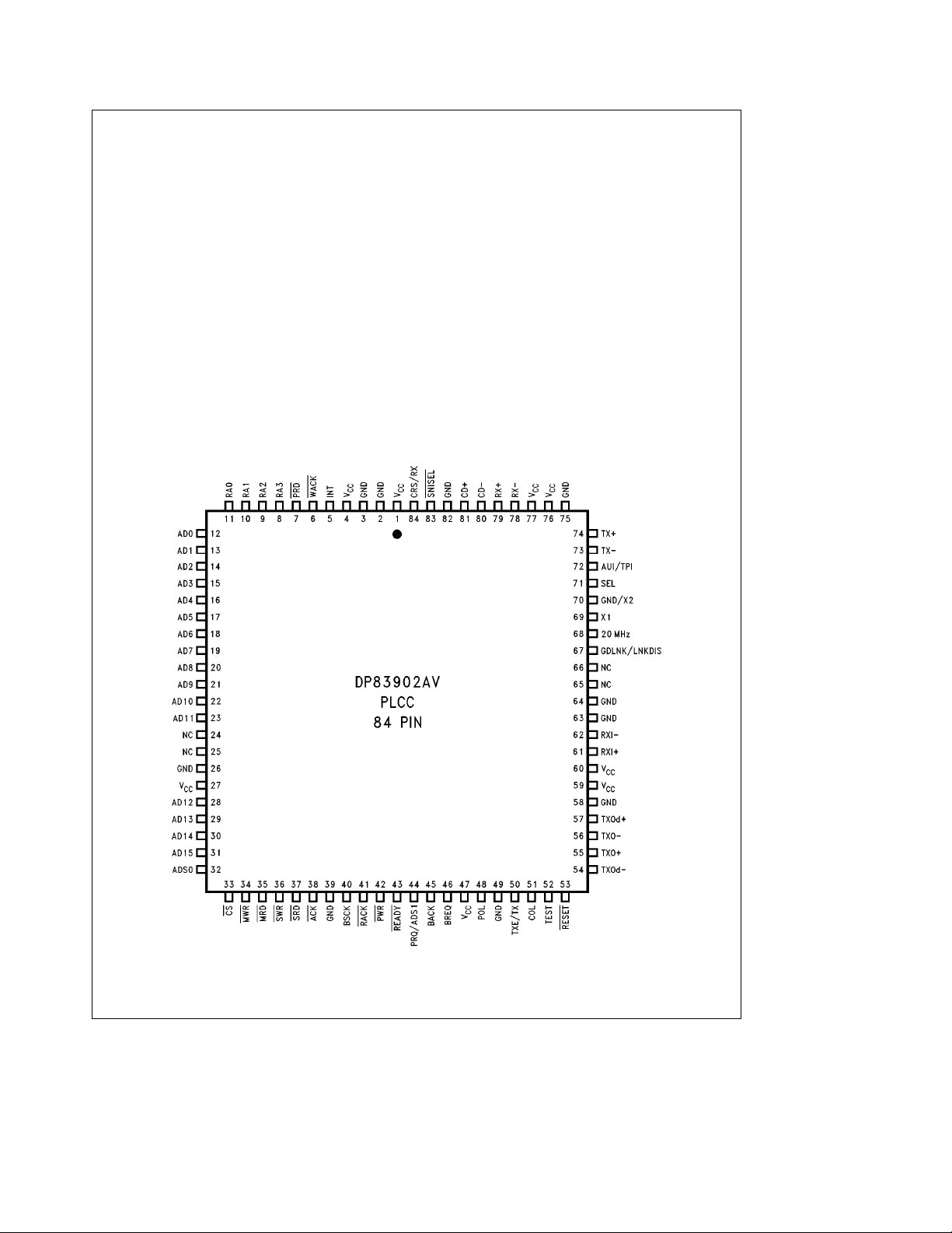
Connection Diagrams
Table Of Contents
1.0 SYSTEM DIAGRAM
2.0 PIN DESCRIPTION
3.0 BLOCK DIAGRAM
4.0 FUNCTIONAL DESCRIPTION
5.0 TRANSMIT/RECEIVE PACKET
ENCAPSULATION/DECAPSULATION
6.0 DIRECT MEMORY ACCESS CONTROL (DMA)
7.0 PACKET RECEPTION
8.0 PACKET TRANSMISSION
9.0 REMOTE DMA
10.0 INTERNAL REGISTERS
11.0 INITIALIZATION PROCEDURES
12.0 LOOPBACK DIAGNOSTICS
13.0 BUS ARBITRATION AND TIMING
14.0 PRELIMINARY ELECTRICAL CHARACTERISTICS
15.0 SWITCHING CHARACTERISTICS
16.0 AC TIMING TEST CONDITIONS
17.0 PHYSICAL DIMENSIONS
Order Number DP83902AV
See NS Package Number V84A
2
TL/F/11157– 2
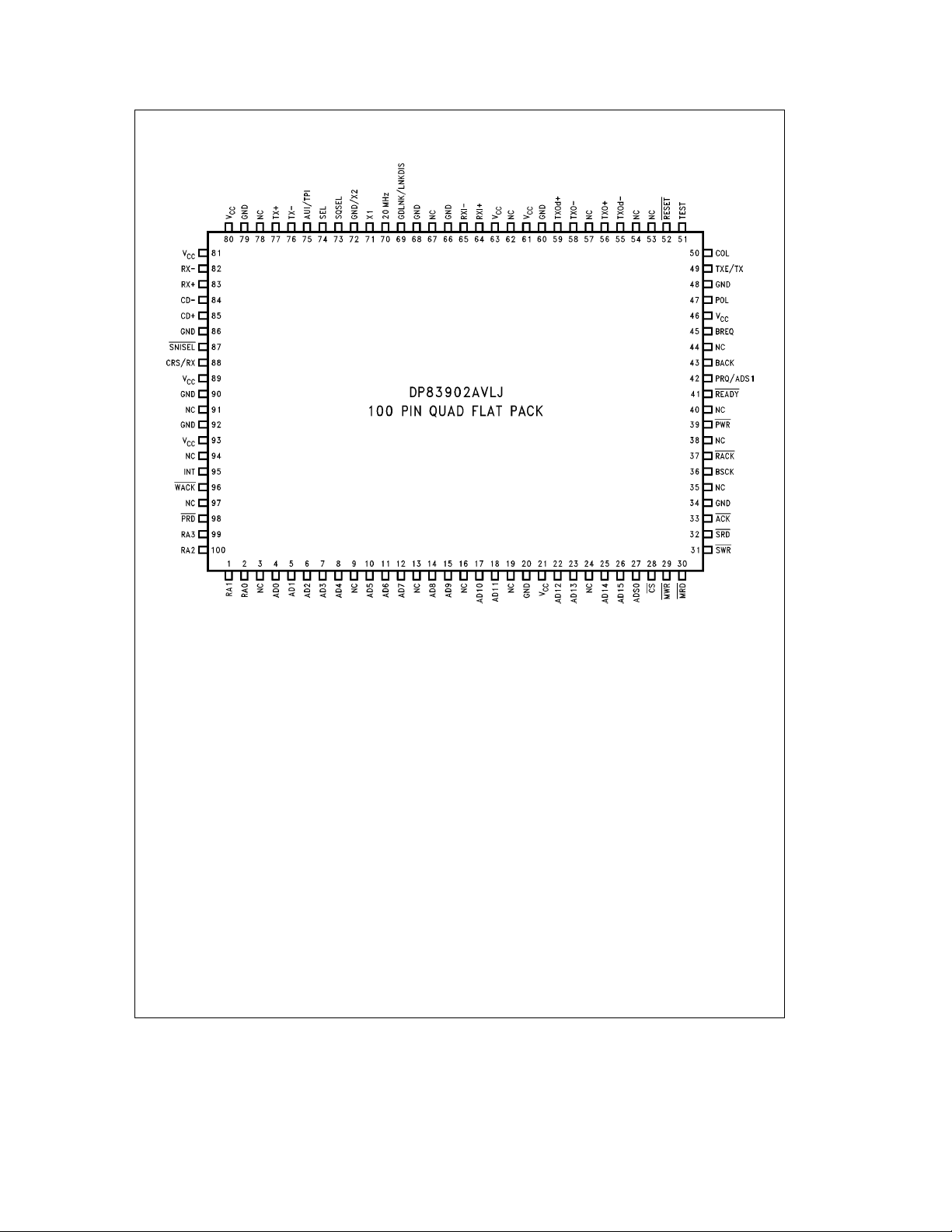
Connection Diagrams (Continued)
Order Number DP83902AVLJ
See NS Package Number VLJ100A
3
TL/F/11157– 56
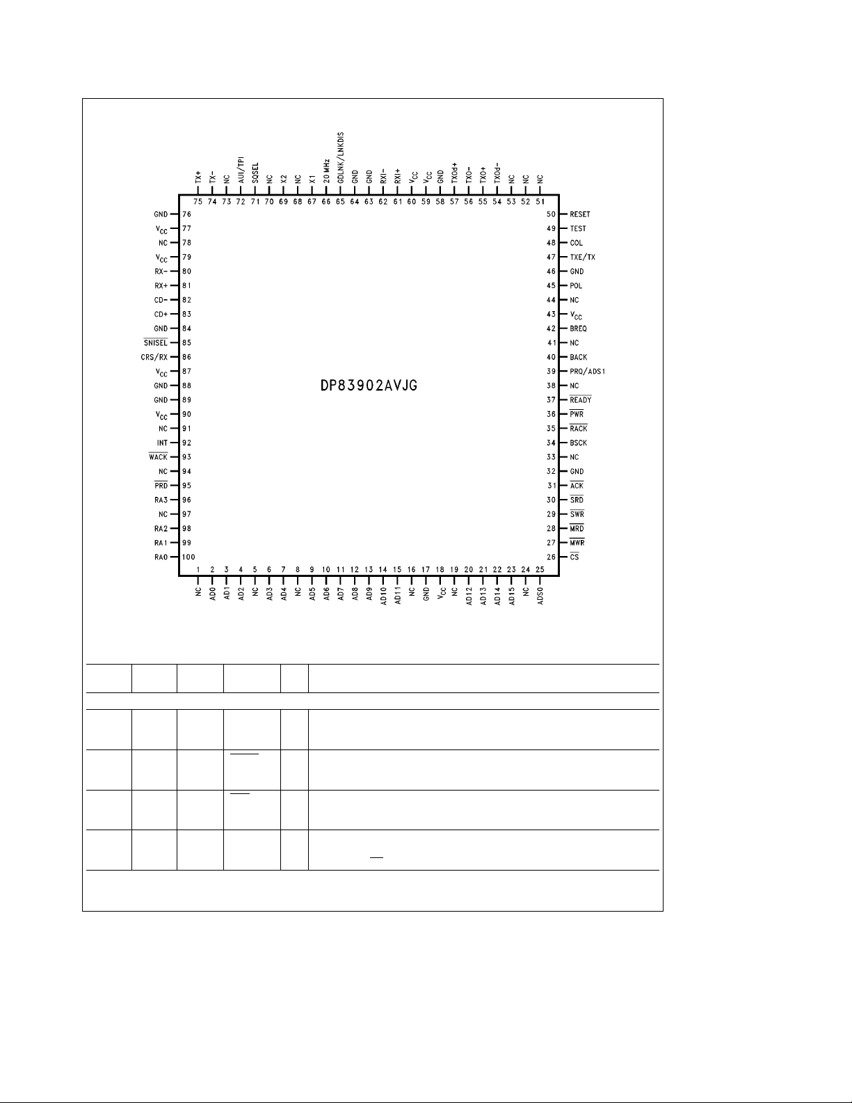
Connection Diagrams (Continued)
Order Number DP83902AVJG
See NS Package Number VJG100A
TL/F/11157– 65
2.0 Pin Description
PQFP PLCC AVJG Pin
Pin No. Pin No. Pin No. Name
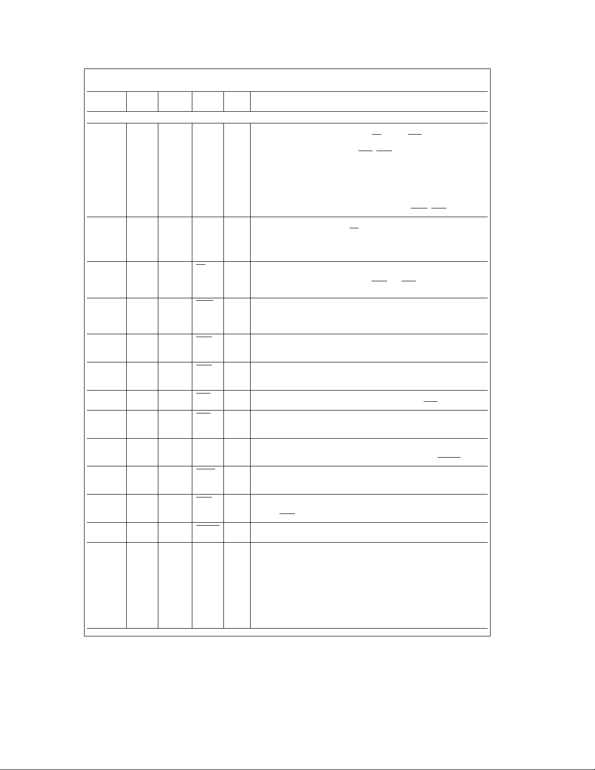
BUS INTERFACE PINS
95 5 92 INT O INTERRUPT: Indicates that the DP83902A requires CPU attention after
96 6 93 WACK I WRITE ACKNOWLEDGE: Issued from system to DP83902A to indicate that
98 7 95 PRD O PORT READ: Enables data from external latch on to local bus during a
99, 100, 8 – 11 96, RA3– RA0 I REGISTER ADDRESS: These four pins are used to select a register to be read
1, 2 98–100 or written. The state of these inputs is ignored when the DP83902A is not in
I/O Description
reception transmission or completion of DMA transfers. The interrupt is cleared
by writing to the ISR (Interrupt Status Register). All interrupts are maskable.
data has been written to the external latch. The DP83902A will begin a write
cycle to place the data in local memory.
memory write cycle to local memory (remote write operation). This allows
asynchronous transfer of data from the system memory to local memory.
slave mode (CS
high).
4
2.0 Pin Description (Continued)
PQFP PLCC AVJG Pin
Pin No. Pin No. Pin No. Name
BUS INTERFACE PINS (Continued)
4–8, 12 – 23, 2– 4, 6, AD0– I/O, Z MULTIPLEXED ADDRESS/DATA BUS:
10–12, 28–31 7, 9 – 15, AD15
14, 15, 17, 20–23 DP83902A, pins AD0–AD7 are used to read and write register data. AD8–
18, 22, 23, AD15 float during I/O transfers, SRD
25, 26 direction of transfer.
27 32 25 ADS0 I/O, Z ADDRESS STROBE 0:
28 33 26 CS I CHIP SELECT: Chip Select places controller in slave mode for mP access to
29 34 27 MWR O, Z MASTER WRITE STROBE: (Strobe for DMA transfers)
30 35 28 MRD O, Z MASTER READ STROBE: (Strobe for DMA transfers)
31 36 29 SWR I SLAVE WRITE STROBE: Strobe from CPU to write an internal register
32 37 30 SRD I SLAVE READ STROBE: Strobe from CPU to read an internal register
33 38 31 ACK O ACKNOWLEDGE: Active low when DP83902A grants access to CPU. Used
36 40 34 BSCK I BUS CLOCK: This clock is used to establish the period of the DMA memory
37 41 35 RACK I READ ACKNOWLEDGE: Indicates that the system DMA or host CPU has
39 42 36 PWR O PORT WRITE: Strobe used to latch data from the DP83902A into external
41 43 37 READY I READY: This pin is set high to insert wait states during a DMA transfer. The
42 44 39 PRQ/ O, Z PORT REQUEST/ADDRESS STROBE 1
ADS1
I/O Description
Register Access, with DMA inactive, CS low and ACK returned from
#
, SWR pins are used to select
Bus Master with BACK input asserted.
#
During t1 of memory cycle AD0–AD15 contain address.
During t2, t3, t4 AD0–AD15 contain data (word transfer mode).
During t2, t3, t4 AD0–AD7 contain data, AD8–AD15 contain address (byte
transfer mode).
Direction of transfer is indicated by DP83902A on MWR
Input: with DMA inactive and CS low, latches RA0–RA3 inputs on falling
#
edge. If high, data present on RA0–RA3 will flow through latch.
Output: When Bus Master, latches address bits (AD0–AD15) to external
#
memory during DMA transfers.
internal registers. Must be valid through data portion of bus cycle. RA0–RA3
are used to select the internal register. SWR
data transfer.
Active low during write cycles (t2, t3, tw) to buffer memory. Rising edge
coincides with the presence of valid output data. TRI-STATE
asserted.
Active during read cycles (t2, t3, tw) to buffer memory. Input data must be
valid on rising edge of MRD. TRI-STATE until BACK asserted.
selected by RA0–RA3. Data is latched into the DP83902A on the rising
edge of this input.
selected by RA0–RA3. The register data is output when SRD goes low.
to insert WAIT states to CPU until DP83902A is synchronized for a register
read or write operation.
cycle. Four clock cycles (t1, t2, t3, t4) are used per DMA cycle. DMA
transfers can be extended by one BSCK increment using the READY
read the data placed in the external latch by the DP83902A. The DP83902A
will begin a read cycle to update the latch.
latch for transfer to host memory during Remote Read transfers. The rising
edge of PWR
DP83902A will sample this signal at t3 during DMA transfers.
32-BIT MODE: If LAS is set in the Data Configuration Register, this line is
#
programmed as ADS1. It is used to strobe addresses A16–A31 into
external latches. (A16–A31 are the fixed addresses stored in RSAR0,
RSAR1). ADS1 will remain at TRI-STATE until BACK is received.
16-BIT MODE: If LAS is not set in the Data Configuration Register, this
#
line is programmed as PRQ and is used for Remote DMA Transfers. The
DP83902A initiates a single remote DMA read or write operation by
asserting this pin. In this mode PRQ will be a standard logic output.
Note: This line will power up as TRI-STATE until the Data Configuration Register is programmed.
coincides with the presence of valid data on the local bus.
and SRD select direction of
, MRD lines.
until BACK
É
input.
5

2.0 Pin Description (Continued)
PQFP PLCC AVJG Pin
Pin No. Pin No. Pin No. Name
BUS INTERFACE PINS (Continued)
43 45 40 BACK I BUS ACKNOWLEDGE: Bus Acknowledge is an active high signal indicating that
45 46 42 BREQ O BUS REQUEST: Bus Request is an active high signal used to request the bus for
52 53 50 RESET I RESET: Reset is active low and places the DP83902A in a reset mode
NETWORK INTERFACE PINS
47 48 45 POL O POLARITY: A TTL/MOS active high output. This signal is normally in the low
49 50 47 TXE/TX O TRANSMIT ENABLE/TRANSMIT: A TTL/MOS active high output. It is asserted
50 51 48 COL O COLLISION: A TTL/MOS active high output. It is asserted for approximately 50
51 52 49 TEST I FACTORY TEST INPUT: Used to check the chip’s internal functions. This should
55, 56, 54, 55, 54, 55, TXOdb,OTWISTED PAIR TRANSMIT OUTPUTS: These high drive CMOS level outputs
58, 59 56, 57 56, 57 TXO
TXO
TXOd
64, 65 61, 62 61, 62 RXIa,ITWISTED PAIR RECEIVE INPUTS: These inputs feed a differential amplifier
RXI
69 67 65 GDLNK/ I/O GOOD LINK/LINK DISABLE: This pin has a dual function both input and output.
LNKDIS The function is latched by the DP83902A on the rising edge of the Reset signal
73 Ð 70 SQSEL I TPI SQUELCH SELECT: This pin selects the TPI module input squelch
70 68 66 20 MHz O 20 MHz: This is a TTL/MOS level signal. It is a buffered version of the oscillator
71 69 67 X1 I EXTERNAL OSCILLATOR INPUT
72 70 69 GND/ I GROUND/X2: If an oscillator is used, this pin should be tied to ground and if a
X2 crystal is used, this pin should be tied directly to the crystal.
74 71 71 SEL I MODE SELECT: When high, TXaand TXbare the same voltage in the idle
I/O Description
the CPU has granted the bus to the DP83902A. If immediate bus access is
desired, BREQ should be tied to BACK. Tying BACK to V
deadlock.
will result in a
CC
DMA transfers. This signal is automatically generated when the FIFO needs
servicing.
immediately. No packets are transmitted or received by the DP83902A until STA
bit is set. Affects Command Register, Interrupt Mask Register, Data Configuration
Register and Transmit Configuration Register. The DP83902A will execute reset
within 10 BSCK cycles.
state. When the TPI module detects seven consecutive link pulses or three
consecutive received packets with reversed polarity POL, is asserted.
for approximately 50 ms whenever the DP83902A transmits data in either AUI or
TPI modes.
ms whenever the DP83902A detects a collision in either the AUI or TPI modes.
be tied low during normal operation.
a
, are resistively combined external to the chip to produce a differential output
b
, signal with equalization to compensate for Intersymbol Interference (ISI) on the
a
b
twisted pair medium.
which passes valid data to the ENDEC module.
i.e.: on the chip returning to normal operation after reset.
As an output this pin is configured as an open drain N-channel device and is
suitable for driving a LED. It will be latched as output on removal of chip reset if
connected to a LED or left open circuit. Under normal conditions (the twisted pair
link is not broken) the output will be low, and the LED will be lit. The open drain
output will be switched off if the twisted pair link has been detected to be broken.
It is recommended that the color of the LED be green. This output will be pulled
high in AUI mode, by an internal resistor of approximately 15 kX.
When this pin, which has an internal pull-up resistor to V
an input and the link integrity checking is disabled.
thresholds. When tied low, the input squelch threshold on the RXI
, is tied low it becomes
DD
g
inputs
complies to 10BASE-T specification. When set high, the RXIginput operates
with reduced squelch levels, allowing its use with longer lengths of cable or cable
with higher losses. If this pin is left unconnected, an internal pulldown causes the
ST-NIC’s TPI to default to the higher squelch level.
X2. It is suitable to drive external logic.
state. When low, Transmit
a
is positive with respect to Transmitbin the idle
state, at the transformer’s primary.
6

2.0 Pin Description (Continued)
PQFP PLCC AVJG Pin
Pin No. Pin No. Pin No. Name
NETWORK INTERFACE PINS (Continued)
75 72 72 AUI/ I AUI/TPI SELECT: A TTL level active high input that selects either the
TPI AUI interface or the TPI module for interface with the ENDEC module.
76, 77 73, 74 74, 75 TXb,OAUI TRANSMIT OUTPUT: Differential driver which sends the encoded
TX
82, 83 78, 79 80, 81 RXb,IAUI RECEIVE INPUT: Differential receive input pair from the
RX
84, 85 80, 81 82, 83 CDb,IAUI COLLISION INPUT: Differential collision pair input from the
CD
87 83 85 SNISEL I FACTORY TEST INPUT: For normal operation tied to VCC. When low
88 84 86 CRS/ O CARRIER SENSE/RECEIVE: A TTL/MOS level active high signal. It is
RX asserted for approximately 50 ms whenever valid transmit or receive
POWER SUPPLY PINS (DIGITAL)
21, 46, 89 1, 27, 47 18, 43, 87 V
20, 34, 48, 2, 26, 39, 17, 32, 46, GND NEGATIVE (GROUND) SUPPLY PINS: It is suggested that a
68, 90 49, 64 64, 88 decoupling capacitor be connected between the V
POWER SUPPLY PINS (ANALOG)
93 4 90 V
92 3 89 GND VCO GROUND SUPPLY PIN: Care should be taken to reduce noise on
63 60 60 V
66 63 63 GND TPI RECEIVE GROUND: Ground pin for the Twisted Pair Interface
61 59 59 V
60 58 58 GND TPI TRANSMIT GROUND: Ground pin for the Twisted Pair Interface
81 77 79 V
86 82 84 GND AUI RECEIVE GROUND: Ground pin for the AUI Interface Receiver.
80 76 77 V
79 75 76 GND AUI TRANSMIT GROUND: Ground pin for the AUI Interface
NO CONNECTION
3, 9, 13, 16, 24, 25, 1, 5, 8, 16, NC NO CONNECTION. Do not connect to these pins.
19, 24, 35, 38, 65, 66 19, 24, 33,
40, 44, 53, 54, 38, 41, 44,
57, 62, 67, 78, 51, 52, 53,
91, 94, 97 68, 70, 73,
78, 91, 94,
97
I/O Description
When high the AUI is selected, when low the TPI is selected.
a
data to the transceiver. The outputs are source followers which require
270X pulldown resistors.
a
a
transceiver.
transceiver.
enables the ENDEC module to be tested independently of the
DP83902A module.
data is detected while in AUI mode or receive data is detected while in
TPI mode.
CC
CC
POSITIVE 5V SUPPLY PINS
VCO 5V SUPPLY PIN: Care should be taken to reduce noise on this
pin as it supplies power to the analog VCO to the Phase Lock Loop.
this pin as it supplies ground to the analog VCO to the Phase Lock
Loop.
CC
TPI RECEIVE 5V SUPPLY: Power pin supplies 5V to the Twisted Pair
Interface Receiver.
Receiver.
CC
TPI TRANSMIT 5V SUPPLY: Power pin supplies 5V to the Twisted Pair
Interface Transmitter.
Transmitter.
CC
CC
AUI RECEIVE 5V SUPPLY: Power pin supplies 5V to the AUI Interface
Receiver.
AUI TRANSMIT 5V SUPPLY: Power pin supplies 5V to AUI Interface
Transmitter.
Transmitter.
and GND pins.
CC
7
3.0 Block Diagram
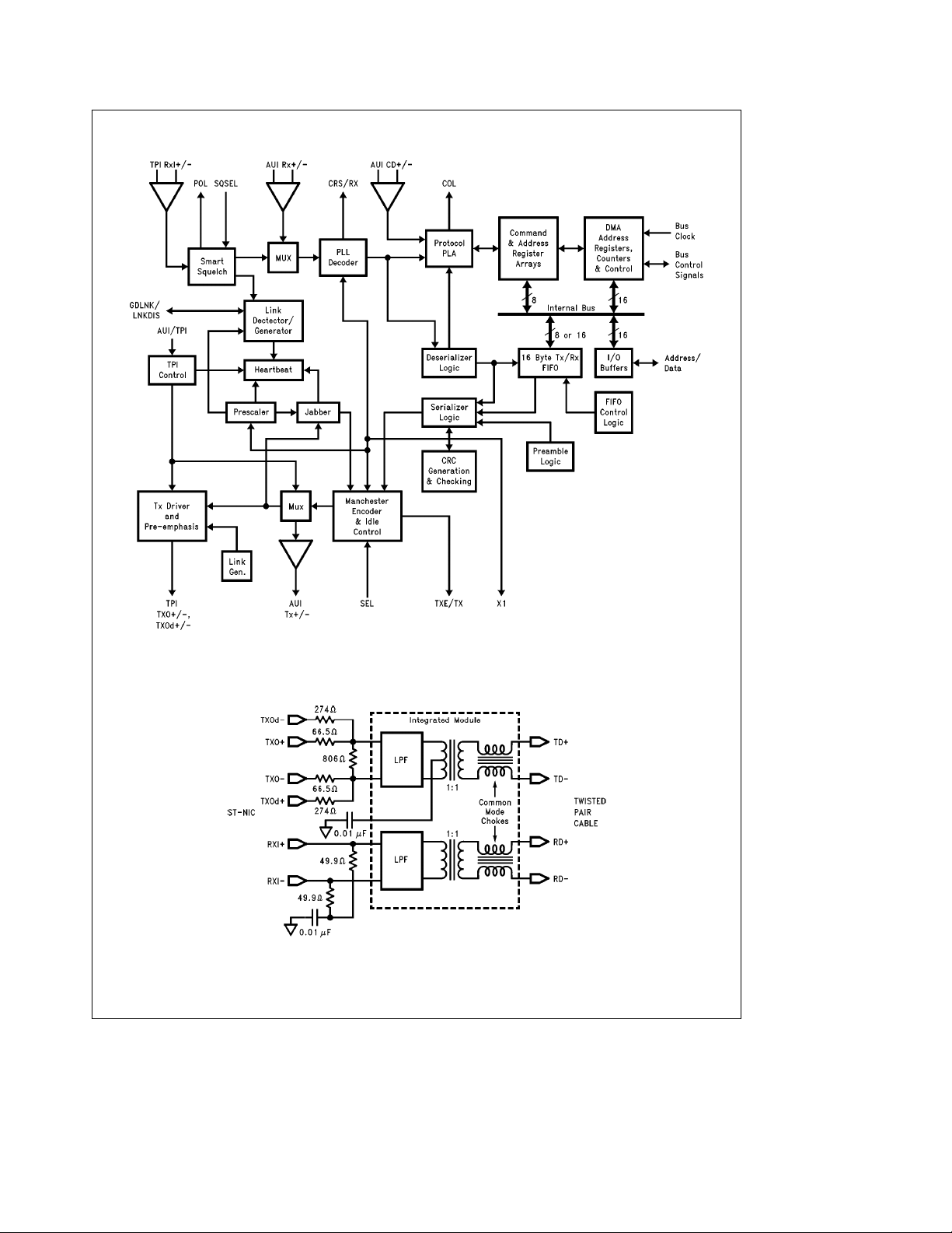
FIGURE 1
Typical Connection to Twisted Pair Cable
Recommended integrated modules are:
1) Pulse Engineering PE65431
2) Belfuse 0556-2006-01 or 0556-3392-00
3) Valor FL1012.
ST-NIC Twisted Pair Interface
8
TL/F/11157– 3
TL/F/11157– 4
4.0 Functional Description (Refer to
Figure 1
TWISTED PAIR INTERFACE (TPI) MODULE
The TPI consists of five main logical functions:
a) The Smart Squelch, responsible for determining when
valid data is present on the differential receive inputs
g
(RXI
).
b) The Collision function checks for simultaneous transmis-
sion and reception of data on the TXO
c) The Link Detector/Generator checks the integrity of the
cable connecting the two twisted pair MAUs.
d) The Jabber disables the transmitter if it attempts to trans-
mit a longer than legal packet.
e) The Tx Driver & Pre-emphasis transmits Manchester en-
coded data to the twisted pair network via the summing
resistors and transformer/filter.
SMART SQUELCH
The ST-NIC implements an intelligent receive squelch on
g
the RXI
differential inputs to ensure that impulse noise on
the receive inputs will not be mistaken for a valid signal.
The squelch circuitry employs a combination of amplitude
and timing measurements to determine the validity of data
on the twisted pair inputs. There are two squelch levels
which are selectable via the SQSEL pin. One mode is
10BASE-T compatible, and the second is reduced squelch
mode.
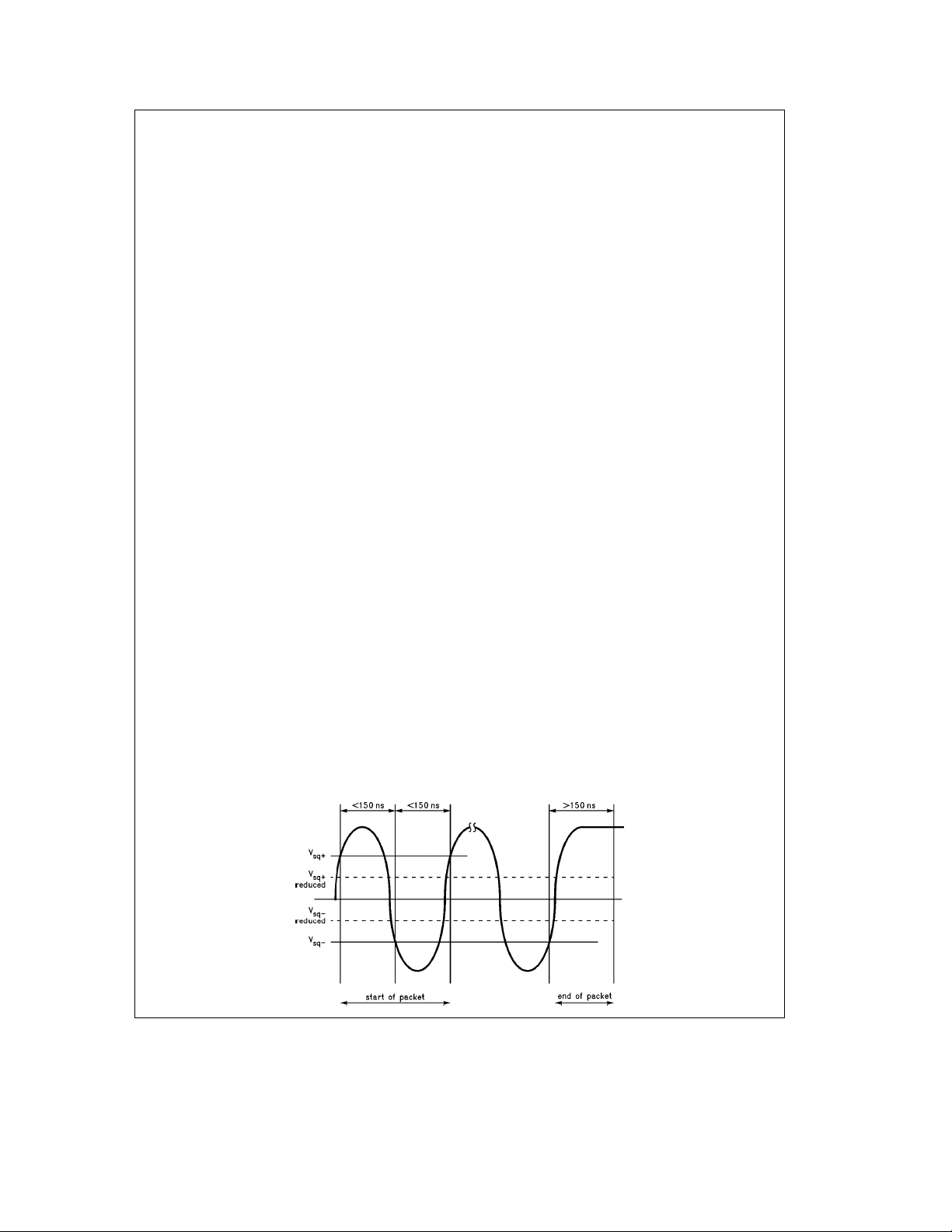
The diagram shows the 10BASE-T mode operation of the
smart squelch.
The signal at the start of packet is checked by the smart
squelch and any pulses not exceeding the squelch level
(either positive or negative, depending upon polarity) will be
rejected. Once this first squelch level is overcome correctly
the opposite squelch level must then be exceeded within
150 ns. Finally the signal must exceed the original squelch
level within a further 150 ns to ensure that the input waveform will not be rejected. The checking procedure results in
the loss of typically three bits at the beginning of each packet.
Only after all these conditions have been satisfied will a
control signal be generated to indicate to the remainder of
the circuitry that valid data is present. At this time the smart
squelch circuitry is reset.
Valid data is considered to be present until either squelch
level has not been generated for a time longer than 150 ns,
indicating End of Packet. Once good data has been detected the squelch levels are reduced to minimize the effect of
noise causing premature End of Packet detection.
g
and RXIgpins.
)
The reduced squelch mode functions the same as the
10BASE-T mode except that only the lower level is used for
both turn-on and turn-off.
COLLISION
A collision is detected by the TPI module when the receive
and transmit channels are active simultaneously. If the TPI
is receiving when a collision is detected it is reported to the
controller immediately. If, however, the TPI is transmitting
when a collision is detected the collision is not reported until
seven bits have been received while in the collision state.
This prevents a collision being reported incorrectly due to
noise on the network. The signal to the controller remains
for the duration of the collision.
Approximately 1 ms after the transmission of each packet a
signal called the Signal Quality Error (SQE) consisting of
typically 10 cycles of 10 MHz is generated. This 10 MHz
signal, also called the Heartbeat, ensures the continued
functioning of the collision circuitry.
LINK DETECTOR/GENERATOR
The link generator is a timer circuit that generates a link
pulse as defined by the 10BASE-T specification that will be
generated by the transmitter section. The pulse which is
100 ns wide is transmitted on the TXO
a
output, every
16 ms, in the absence of transmit data.
The pulse is used to check the integrity of the connection to
the remote MAU. The link detection circuit checks for valid
pulses from the remote MAU and if valid link pulses are not
received the link detector will disable the transmit, receive
and collision detection functions.
The GDLNK output can directly drive a LED to show that
there is a good twisted pair link. For normal conditions the
LED will be on. The link integrity function can be disabled as
described in the Pin Description Section.
JABBER
The jabber timer monitors the transmitter and disables the
transmission if the transmitter is active for greater than
26 ms. The transmitter is then disabled for the whole time
that the ENDEC module’s internal transmit enable is asserted. This signal has to be deasserted for approximately
750 ms (the unjab time) before the Jabber re-enables the
transmit outputs.
TRANSMIT DRIVER
The transmitter consists of four signals, the true and complement Manchester encoded data (TXO
nals delayed by 50 ns (TXOd
g
).
g
) and these sig-
TL/F/11157– 5
9
4.0 Functional Description (Continued)
a
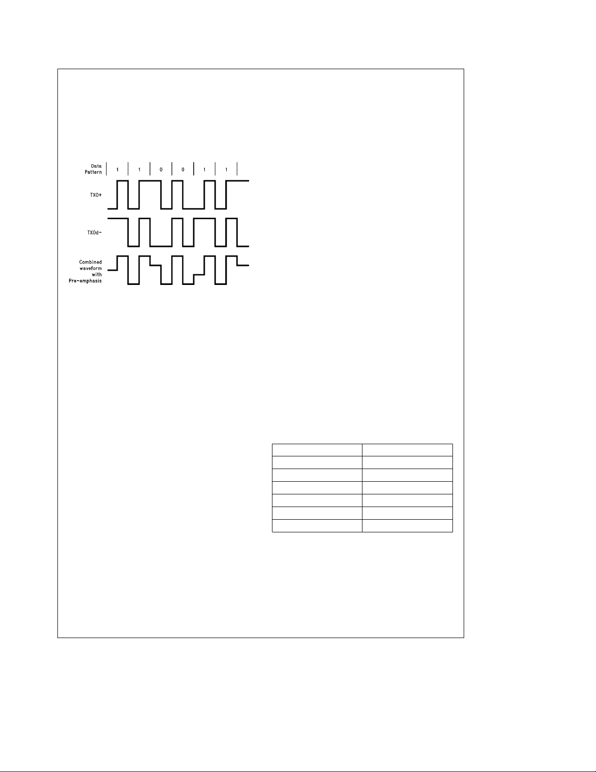
These four signals are resistively combined, TXO
b
TXOd
and TXObwith TXOda. This is known as digital
pre-emphasis and is required to compensate for the twisted
pair cable which acts like a low pass filter causing greater
attenuation to the 10 MHz (50 ns) pulses of the Manchester
encoded waveform than the 5 MHz (100 ns) pulses.
An example of how these signals are combined is shown in
the following diagram.
The signal with pre-emphasis shown above is generated by
resistively combining TXO
a
and TXOdb. This signal along
with its complement is passed to the transmit filter.
STATUS INFORMATION
Status information is provided by the ST-NIC on the
CRS/RX, TXE/TX, COL and POL outputs as described in
the pin description table. These outputs are suitable for driving status LEDs via an appropriate driver circuit.
The POL output is normally low, and will be driven high
when seven consecutive link pulses or three consecutive
receive packets are detected with reversed polarity. A polarity reversal can be caused by a wiring error at either end of
the TPI cable. On detection of a polarity reversal the condition is latched and POL is asserted. The TPI corrects for this
error internally and will decode received data correctly, eliminating the need to correct the wiring error.
ENCODER/DECODER (ENDEC) MODULE
The ENDEC consists of three main logical blocks:
a) The Manchester encoder accepts NRZ data from the
controller, encodes the data to Manchester, and transmits it differentially to the transceiver, through the differential transmit driver.
b) The Manchester decoder receives Manchester data from
the transceiver, converts it to NRZ data and clock pulses,
and sends it to the controller.
c) The collision translator indicates to the controller the
presence of a valid 10 MHz collision signal to the PLL.
MANCHESTER ENCODER AND DIFFERENTIAL DRIVER
The differential transmit pair, on the secondary of the transformer, drives up to 50 meters of twisted pair AUI cable.
These outputs are source followers which require two 270X
pull-down resistors to ground.
The DP83902A allows both half-step and full-step to be
compatible with Ethernet and IEEE 802.3. With the SEL pin
low (for Ethernet I). Transmit
a
is positive with respect to
with
TL/F/11157– 6
b
Transmit
Transmit
during idle; with SEL high (for IEEE 802.3),
a
and Transmitbare equal in the idle state. This
provides zero differential voltage to operate with transformer coupled loads.
MANCHESTER DECODER
The decoder consists of a differential receiver and a PLL to
separate a Manchester decoded data stream into internal
clock signals and data. The differential input must be externally terminated with two 39X resistors connected in series
if the standard 78X transceiver drop cable is used. In thin
Ethernet applications, these resistors are optional. To prevent noise from falsely triggering the decoder, a squelch
circuit at the input rejects signals with levels less than
b
175 mV. Signals more negative thanb300 mV are decoded. Data becomes valid typically within 5 bit times. The
DP83902A may tolerate bit jitter up to 18 ns in the received
data. The decoder detects the end of a frame when no more
mid-bit transitions are detected.
COLLISION TRANSLATOR
When in AUI mode, when the Ethernet transceiver (DP8392
CTI) detects a collision, it generates a 10 MHz signal to the
differential collision inputs (CD
g
) of the DP83902A. When
these inputs are detected active, the DP83902A uses this
signal to back off its current transmission and reschedule
another one.
The collision differential inputs are terminated the same way
as the differential receive inputs. The squelch circuitry is
also similar, rejecting pulses with levels less than
b
175 mV.
CRYSTAL/OSCILLATOR OPERATION
OCSILLATOR
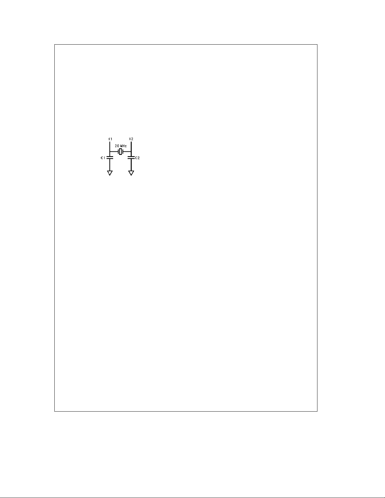
The oscillator is controlled by a 20 MHz parallel resonant
crystal connected between X1 and X2 or by an external
clock on X1. The 20 MHz output of the oscillator is divided
by 2 to generate the 10 MHz transmit clock for the controller. The oscillator also provides internal clock signals to the
encoding and decoding circuits.
Note: When X1 is being driven by an external oscillator, X2 MUST be
grounded.
Crystal Specifications
Resonant Frequency 20 MHz
Tolerance
Stability
Type AT Cut
Circuit Parallel Resonance
Max ESR 25X
Crystal Load Capacitor 20 pF
The 20 MHz crystal connection to the DP83902 requires
special care. The IEEE 802.3 standard requires the transmitted signal frequency to be accurate within
Stray capacitance can shift the crystal’s frequency out of
range and cause transmitted frequency to exceed its 0.01%
tolerance. The frequency marked on the crystal is usually
measured with a fixed load capacitance specified in the
crystal’s data sheet, typically 20 pF.
g
0.005% at 25§C
g
0.005% at 0§C–70§C
g
0.01%.
10
4.0 Functional Description (Continued)
In order to prevent distortion on the transmitted frequency,
the total capacitance seen by the crystal should equal the
total load capacitance. On a standard parallel set-up as
shown in the diagram below, the 2 load caps C1 and C2
should equal 2C1, the spec load cap, (due to the capacitors
acting in series) less any stray capacitances.
Thus the trim capacitors required can be calculated as follows:
e
C1
2XC1b(Cb1aCd1) Where Cb1eBoard cap on X1
e
and Cd1
e
C2
and Cd2
The value of STNIC pins X1 and X2 is in the region of 5 pF.
NIC (Media Access Control) MODULE
RECEIVE DESERIALIZER
The Receive Deserializer is activated when the input signal
Carrier Sense is asserted to allow incoming bits to be shifted into the shift register by the receive clock. The serial
receive data is also routed to the CRC generator/checker.
The Receive Deserializer includes a synch detector which
detects the SFD (Start of Frame Delimiter) to establish
where byte boundaries within the serial bit stream are located. After every eight receive clocks, the byte wide data is
transferred to the 16-byte FIFO and the Receive Byte Count
is incremented. The first six bytes after the SFD are
checked for valid comparison by the Address Recognition
Logic. If the Address Recognition Logic does not recognize
the packet, the FIFO is cleared.
CRC GENERATOR/CHECKER
During transmission, the CRC logic generates a local CRC
field for the transmitted bit sequence. The CRC encodes all
fields after the SFD. The CRC is shifted out MSB first following the last transmit byte. During reception the CRC logic
generates a CRC field from the incoming packet. This local
CRC is serially compared to the incoming CRC appended to
the end of the packet by the transmitting node. If the local
and received CRC match, a specific pattern will be generated and decoded to indicate no data errors. Transmission
errors result in different pattern and are detected, resulting
in rejection of a packet (if so programmed).
TRANSMIT SERIALIZER
The Transmit Serializer reads parallel data from the FIFO
and serializes it for transmission. The serializer is clocked by
the transmit clock generated internally. The serial data is
also shifted into the CRC generator/checker. At the beginning of each transmission, the Preamble and Synch Generator append 62 bits of 1,0 preamble and a 1,1 synch pattern. After the last data byte of the packet has been serialized the 32-bit FCS field is shifted directly out of the CRC
generator. In the event of a collision the Preamble and
Synch generators are used to generate a 32-bit JAM pattern
of all 1’s.
X1 dev cap
2XC1b(Cb2aCd2) Where Cb2eBoard cap on X2
e
X2 dev cap
TL/F/11157– 52
ADDRESS RECOGNITION LOGIC
The address recognition logic compares the Destination Address Field (first 6 bytes of the received packet) to the Physical address registers stored in the Address Register Array.
If any one of the six bytes does not match the pre-programmed physical address, the Protocol Control Logic rejects the packet. All multicast destination addresses are filtered using a hashing technique. (See register description.)
If the multicast address indexes a bit that has been set in
the filter bit array of the Multicast Address Register Array
the packet is accepted, otherwise it is rejected by the Protocol Control Logic. Each destination address is also checked
for all 1’s which is the reserved broadcast address.
FIFO AND BUS OPERATIONS
Overview
To accommodate the different rates at which data comes
from (or goes to) the network and goes to (or comes from)
the system memory, the ST-NIC contains a 16-byte FIFO for
buffering data between the media. The FIFO threshold is
programmable. When the FIFO has filled to its programmed
threshold, the local DMA channel transfers these bytes (or
words) into local memory. It is crucial that the local DMA is
given access to the bus within a minimum bus latency time;
otherwise a FIFO underrun (or overrun) occurs.
FIFO underruns or overruns are caused by two conditions:
(1) the bus latency is so long that the FIFO has filled (or
emptied) from the network before the local DMA has serviced the FIFO and (2) the bus latency has slowed the
throughput of the local DMA to a point where it is slower
than the network data rate (10 Mbit/sec). This second condition is also dependent upon DMA clock and word width
(byte wide or word wide). The worst case condition ultimately limits the overall bus latency which the ST-NIC can tolerate.
Beginning of Receive
At the beginning of reception, the ST-NIC stores the entire
Address field of each incoming packet in the FIFO to determine whether the address matches the ST-NIC’s Physical
Address Registers or maps to one of its Multicast Registers.
This causes the FIFO to accumulate 8 bytes. Furthermore,
there are some synchronization delays in the DMA PLA.
Thus, the actual time to when BREQ is asserted from the
time the Start of Frame Delimiter (SFD) is detected is
7.8 ms. This operation affects the bus latencies at 2- and
4-byte thresholds during the first receive BREQ since the
FIFO must be filled to 8 bytes (or 4 words) before issuing a
BREQ.
End of Receive
When the end of a packet is detected by the ENDEC module, the ST-NIC enters its end of packet processing sequence, emptying its FIFO and writing the status information
at the beginning of the packet. The ST-NIC holds onto the
bus for the entire sequence. The longest time BREQ may be
extended occurs when a packet ends just as the ST-NIC
performs its last FIFO burst. The ST-NIC, in this case, performs a programmed burst transfer followed by flushing the
remaining bytes in the FIFO, and completes by writing the
header information to memory. The following steps occur
during this sequence.
1. ST-NIC issues BREQ because the FIFO threshold has
been reached.
2. During the burst, packet ends, resulting in BREQ extended.
11
4.0 Functional Description (Continued)
3. ST-NIC flushes remaining bytes from FIFO.
4. ST-NIC performs internal processing to prepare for writing the header.
5. ST-NIC writes 4-byte (2-word) header.
6. ST-NIC de-asserts BREQ.
FIFO Threshold Detection
To assure that no overwriting of data in the FIFO, the FIFO
logic flags a FIFO overrun as the 13th byte is written into the
FIFO, effectively shortening the FIFO to 13 bytes. The FIFO
logic also operates differently in Byte Mode and in Word
Mode. In Byte Mode, a threshold is indicated when the n
byte has entered the FIFO; thus, with an 8-byte threshold,
the ST-NIC issues Bus Request (BREQ) when the 9th byte
has entered the FIFO. For Word Mode, BREQ is not generated until n
4 word threshold (equivalent to an 8-byte threshold), BREQ
is issued when the 10th byte has entered the FIFO.
Beginning of Transmit
Before transmitting, the ST-NIC performs a prefetch from
memory to load the FIFO. The number of bytes prefetched
is the programmed FIFO threshold. The next BREQ is not
issued until after the ST-NIC actually begins transmitting
data, i.e., after SFD.
Reading the FIFO
During normal operation, the FIFO must not be read. The
ST-NIC will not issue an ACKnowledge back to the CPU if
the FIFO is read. The FIFO should only be read during loopback diagnostics.
PROTOCOL PLA
The protocol PLA is responsible for implementing the IEEE
802.3 protocol, including collision recovery with random
backoff. The Protocol PLA also formats packets during
transmission and strips preamble and synch during reception.
DMA AND BUFFER CONTROL LOGIC
The DMA and Buffer Control Logic is used to control two
16-bit DMA channels. During reception, the local DMA
stores packets in a receive buffer ring, located in buffer
memory. During transmission the Local DMA uses programmed pointer and length registers to transfer a packet
from local buffer memory to the FIFO. A second DMA channel is used as a slave DMA to transfer data between the
local buffer memory and the host system. The Local DMA
and Remote DMA are internally arbitrated, with the Local
DMA channel having highest priority. Both DMA channels
use a common external bus clock to generate all required
a
2 bytes have entered the FIFO. Thus, with a
a
bus timing. External arbitration is performed with a standard
bus request, bus acknowledge handshake protocol.
5.0 Transmit/Receive Packet
Encapsulation/Decapsulation
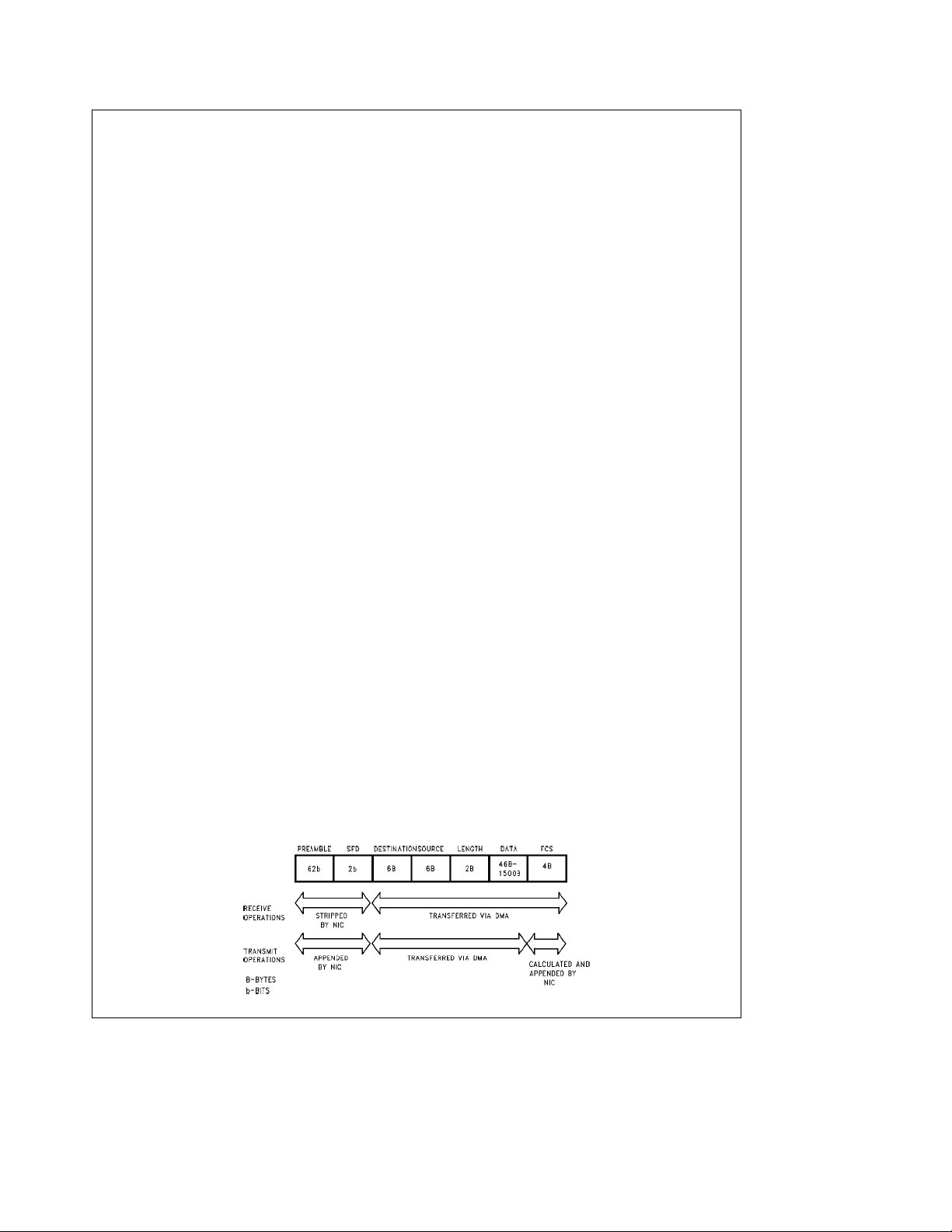
A standard IEEE 802.3 packet consists of the following
fields: preamble, Start of Frame Delimiter (SFD), destination
address, source address, length, data, and Frame Check
Sequence (FCS). The typical format is shown in
The packets are Manchester encoded and decoded by the
ENDEC module and transferred serially to the NIC module
1
using NRZ data with a clock. All fields are of fixed length
except for the data field. The ST-NIC generates and appends the preamble, SFD and FCS field during transmission. The Preamble and SFD fields are stripped during reception. (The CRC is passed through to buffer memory during reception.)
PREAMBLE AND START OF FRAME DELIMITER (SFD)
The Manchester encoded alternating 1,0 preamble field is
used by the ENDEC to acquire bit synchronization with an
incoming packet. When transmitted each packet contains
62 bits of alternating 1,0 preamble. Some of this preamble
will be lost as the packet travels through the network. The
preamble field is stripped by the NIC module. Byte alignment is performed with the Start of Frame Delimiter (SFD)
pattern which consists of two consecutive 1’s. The ST-NIC
does not treat the SFD pattern as a byte, it detects only the
two bit pattern. This allows any preceding preamble within
the SFD to be used for phase locking.
DESTINATION ADDRESS
The destination address indicates the destination of the
packet on the network and is used to filter unwanted packets from reaching a node. There are three types of address
formats supported by the ST-NIC: physical, multicast and
broadcast. The physical address is a unique address that
corresponds only to a single node. All physical addresses
have an MSB of ‘‘0’’. These addresses are compared to the
internally stored physical address registers. Each bit in the
destination address must match in order for the ST-NIC to
accept the packet. Multicast addresses begin with an MSB
of ‘‘1’’. The ST-NIC filters multicast addresses using a standard hashing algorithm that maps all multicast addresses
into a 6-bit value. This 6-bit value indexes a 64-bit array that
filters the value. If the address consists of all 1’s it is a
broadcast address, indicating that the packet is intended for
all nodes. A promiscuous mode allows reception of all packets: the destination address is not required to match any
filters. Physical, broadcast, multicast, and promiscuous address modes can be selected.
Figure 2.
FIGURE 2
12
TL/F/11157– 7
5.0 Transmit/Receive Packet
Encapsulation/Decapsulation
(Continued)
SOURCE ADDRESS
The source address is the physical address of the node that
sent the packet. Source addresses cannot be multicast or
broadcast addresses. This field is simply passed to buffer
memory.
LENGTH/TYPE FIELD
The 2-byte length field indicates the number of bytes that
are contained in the data field of the packet. This field is not
interpreted by the ST-NIC.
DATA FIELD
The data field consists of anywhere from 46 to 1500 bytes.
Messages longer than 1500 bytes need to be broken into
multiple packets. Messages shorter than 46 bytes will require appending a pad to bring the data field to the minimum
length of 46 bytes. If the data field is padded, the number of
valid data bytes is indicated in the length field. The ST-NIC
does not strip or append pad bytes for short packets,
or check for oversize packets.
FCS FIELD
The Frame Check Sequence (FCS) is a 32-bit CRC field
calculated and appended to a packet during transmission to
allow detection of errors when a packet is received. During
reception, error free packets result in a specific pattern in
the CRC generator. Packets with improper CRC will be rejected. The AUTODIN II (X
12
11
a
X
10
a
X
X
polynomial is used for the CRC calculations.
32
26
23
22
a
a
X
8
a
7
a
a
X
X
X
a
X
5
4
a
a
X
16
a
X
X
2
1
a
a
X
X
6.0 Direct Memory Access
Control (DMA)
The DMA capabilities of the ST-NIC greatly simplify the use
of the DP83902A in typical configurations. The local DMA
channel transfers data between the FIFO and memory. On
transmission, the packet is DMAed from memory to the
FIFO in bursts. Should a collision occur (up to 15 times), the
packet is retransmitted with no processor intervention. On
reception, packets are DMAed from the FIFO to the receive
buffer ring (as explained below).
dA remote DMA channel is also provided on the ST-NIC to
accomplish transfers between a buffer memory and system
memory. The two DMA channels can alternatively be combined to form a single 32-bit address with 8- or 16-bit data.
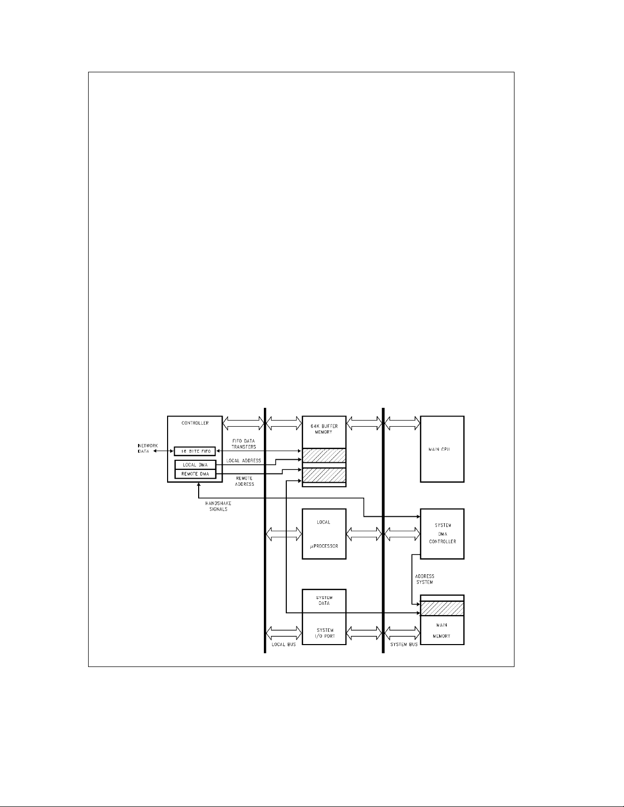
DUAL DMA CONFIGURATION
An example configuration using both the local and remote
DMA channels is shown below. Network activity is isolated
on a local bus, where the ST-NIC’s local DMA channel performs burst transfers between the buffer memory and the
ST-NIC’s FIFO. The Remote DMA transfers data between
the buffer memory and the host memory via a bidirectional
I/O port. The Remote DMA provides local addressing capability and is used as a slave DMA by the host. Host side
addressing must be provided by a host DMA or the CPU.
The ST-NIC allows Local and Remote DMA operations to
be interleaved.
SINGLE CHANNEL DMA OPERATION
a
1)
If desirable, the two DMA channels can be combined to
provide a 32-bit DMA address. The upper 16 bits of the
32-bit address are static and are used to point to a 64 kbyte
(or 32k word) page of memory where packets are to be
received and transmitted.
Dual Bus System
13
TL/F/11157– 8
7.0 Packet Reception
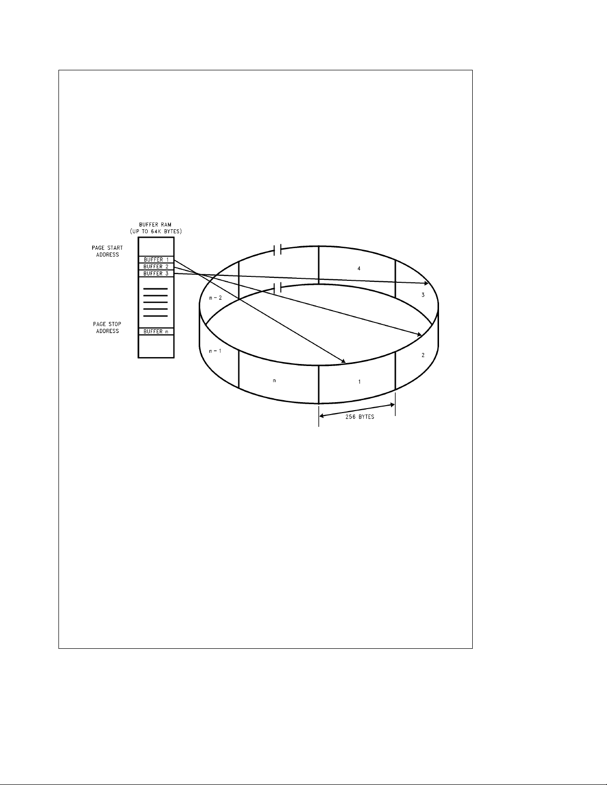
The Local DMA receive channel uses a Buffer Ring Structure comprised of a series of contiguous fixed length
256-byte (128 word) buffers for storage of received packets.
The location of the Receive Buffer Ring is programmed in
two registers, a Page Start and a Page Stop Register. Ethernet packets consist of a distribution of shorter link control
packets and longer data packets, the 256-byte buffer length
provides a good compromise between short packets and
longer packets to most efficiently use memory. In addition
these buffers provide memory resources for storage of
back-to-back packets in loaded networks. The assignment
of buffers for storing packets is controlled by Buffer Management Logic in the ST-NIC. The Buffer Management Log-
ST-NIC Receive Buffer Ring
ic provides three basic functions: linking receive buffers for
long packets, recovery of buffers when a packet is rejected,
and recirculation of buffer pages that have been read by the
host.
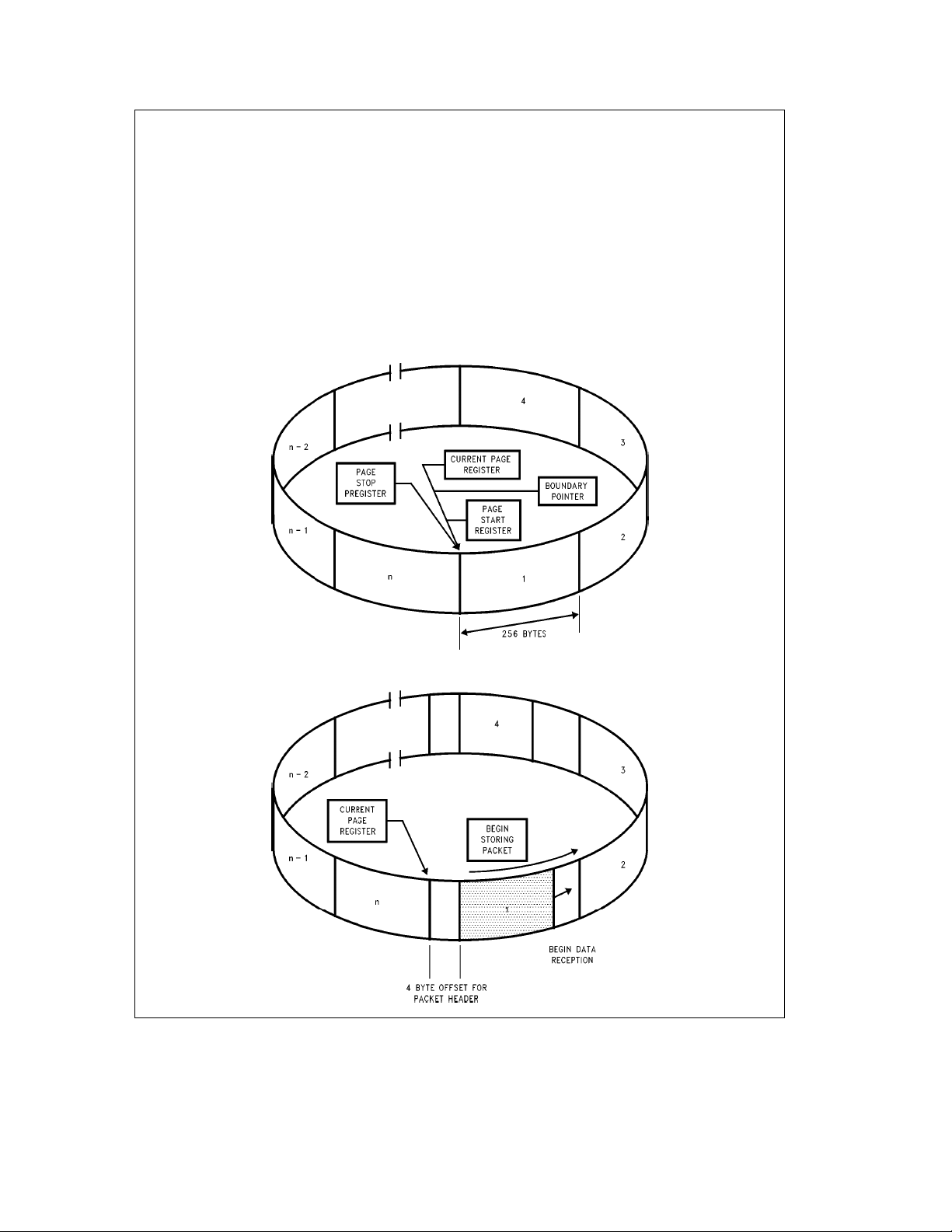
At initialization, a portion of the 64 kbyte (or 32k word) address space is reserved for the receive buffer ring. Two 8-bit
registers, the Page Start Address Register (PSTART) and
the Page Stop Address Register (PSTOP) define the physical boundaries of where the buffers reside. The ST-NIC
treats the list of buffers as a logical ring; whenever the DMA
address reaches the Page Stop Address, the DMA is reset
to the Page Start Address.
TL/F/11157– 9
14
7.0 Packet Reception (Continued)
INITIALIZATION OF THE BUFFER RING
Two static registers and two working registers control the
operation of the Buffer Ring. These are the Page Start Register, Page Stop Register (both described previously), the
Current Page Register and the Boundary Pointer Register.
The Current Page Register points to the first buffer used to
store a packet and is used to restore the DMA for writing
status to the Buffer Ring or for restoring the DMA address in
the event of a Runt packet, a CRC, or Frame Alignment
error. The Boundary Register points to the first packet in the
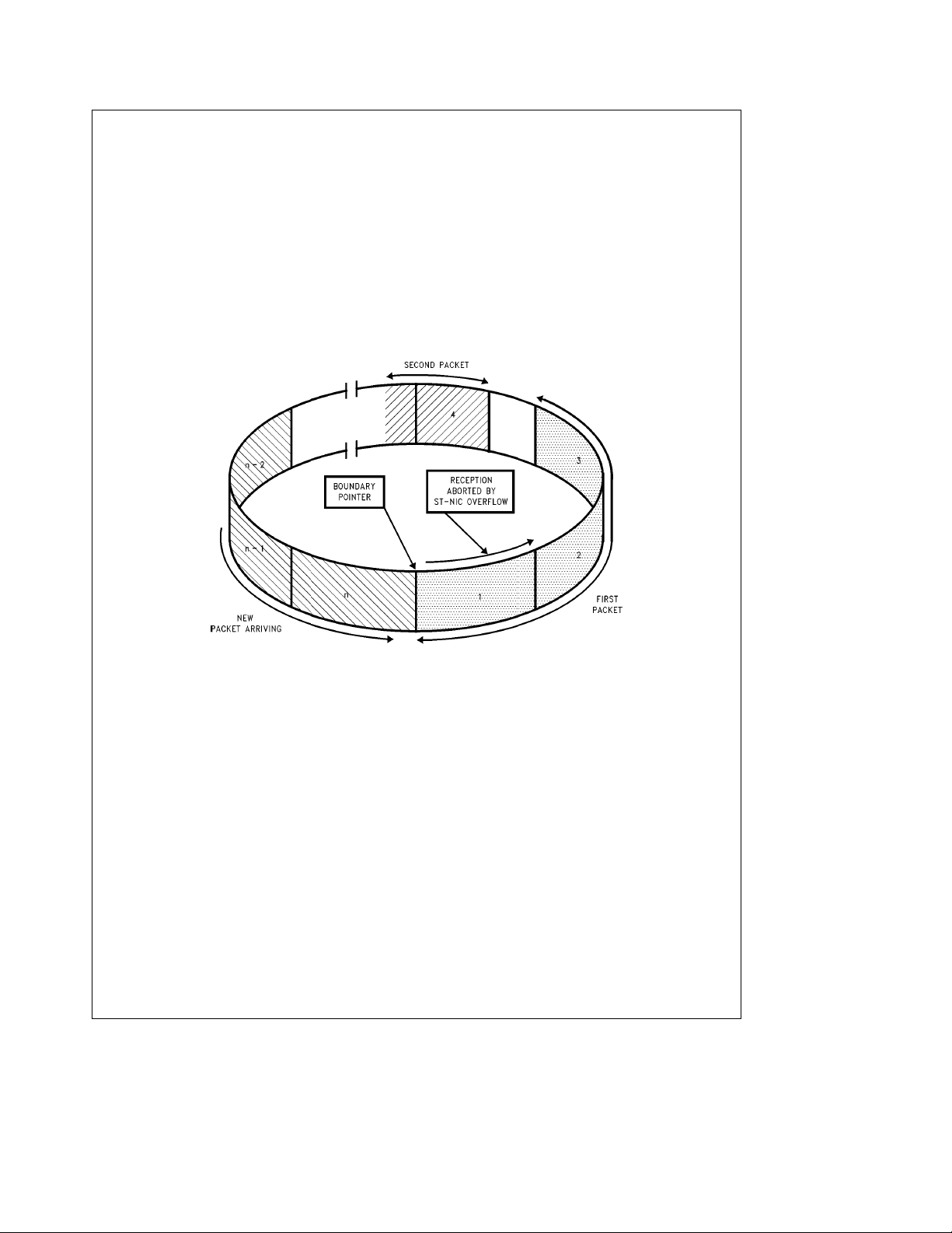
Ring not yet read by the host. If the local DMA address ever
reaches the Boundary, reception is aborted. The Boundary
Pointer is also used to initialize the Remote DMA for remov-
Buffer Ring at Initialization
ing a packet and is advanced when a packet is removed. A
simple analogy to remember the function of these registers
is that the Current Page Register acts as a Write Pointer and
the Boundary Pointer acts as a Read Pointer.
Note: At initialization, the Page Start Register value should be loaded into
both Current Page Register and the Boundary Pointer Register.
Note: The Page Start Register must not be initialized to 00H.
BEGINNING OF RECEPTION
When the first packet begins arriving the ST-NIC begins
storing the packet at the location pointed to by the Current
Page Register. An offset of 4 bytes is saved in this first
buffer to allow room for storing receive status corresponding to this packet.
Received Packet Enters the Buffer Pages
15
TL/F/11157– 10
TL/F/11157– 11
7.0 Packet Reception (Continued)
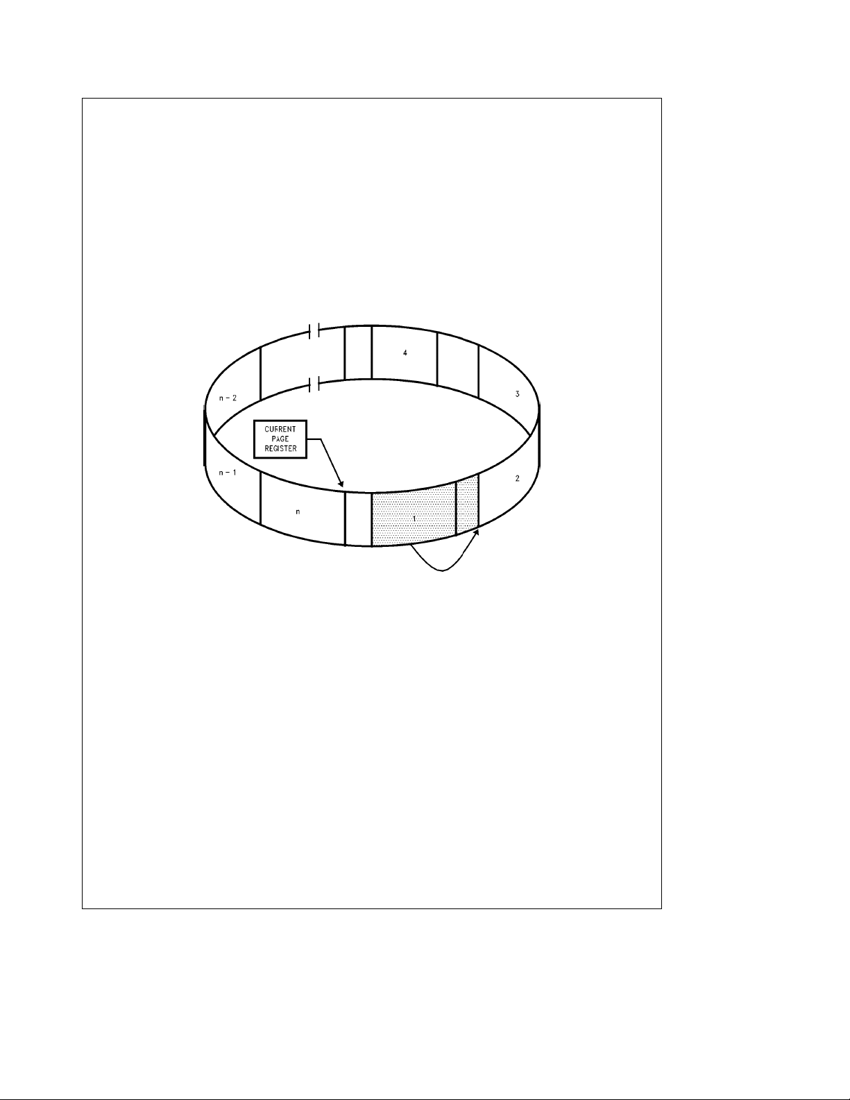
LINKING RECEIVE BUFFER PAGES
If the length of the packet exhausts the first 256-byte buffer,
the DMA performs a forward link to the next buffer to store
the remainder of the packet. For a maximum length packet
the buffer logic will link six buffers to store the entire packet.
Buffers cannot be skipped when linking, therefore a packet
will always be stored in contiguous buffers. Before the next
buffer can be linked, the Buffer Management Logic performs two comparisons. The first comparison tests for
equality between the DMA address of the next buffer and
the contents of the Page Stop Register. If the buffer address equals the Page Stop Register, the buffer management logic will restore the DMA to the first buffer in the
Linking Receive Buffer Pages
Receive Buffer Ring value programmed in the Page Start
Address Register. The second comparison tests for equality
between the DMA address of the next buffer address and
the contents of the Boundary Pointer Register. If the two
values are equal the reception is aborted. The Boundary
Pointer Register can be used to protect against overwriting
any area in the receive buffer ring that has not yet been
read. When linking buffers, buffer management will never
cross this pointer, effectively avoiding any overwrites. If the
buffer address does not match either the Boundary Pointer
or Page Stop Address, the link to the next buffer is performed.
1) Check foreto PSTOP
2) Check for
e
to Boundary
TL/F/11157– 12
16
7.0 Packet Reception (Continued)
Buffer Ring Overflow
If the Buffer Ring has been filled and the DMA reaches the
Boundary Pointer Address, reception of the incoming packet will be aborted by the ST-NIC. Thus, the packets previously received and still contained in the Ring will not be
destroyed.
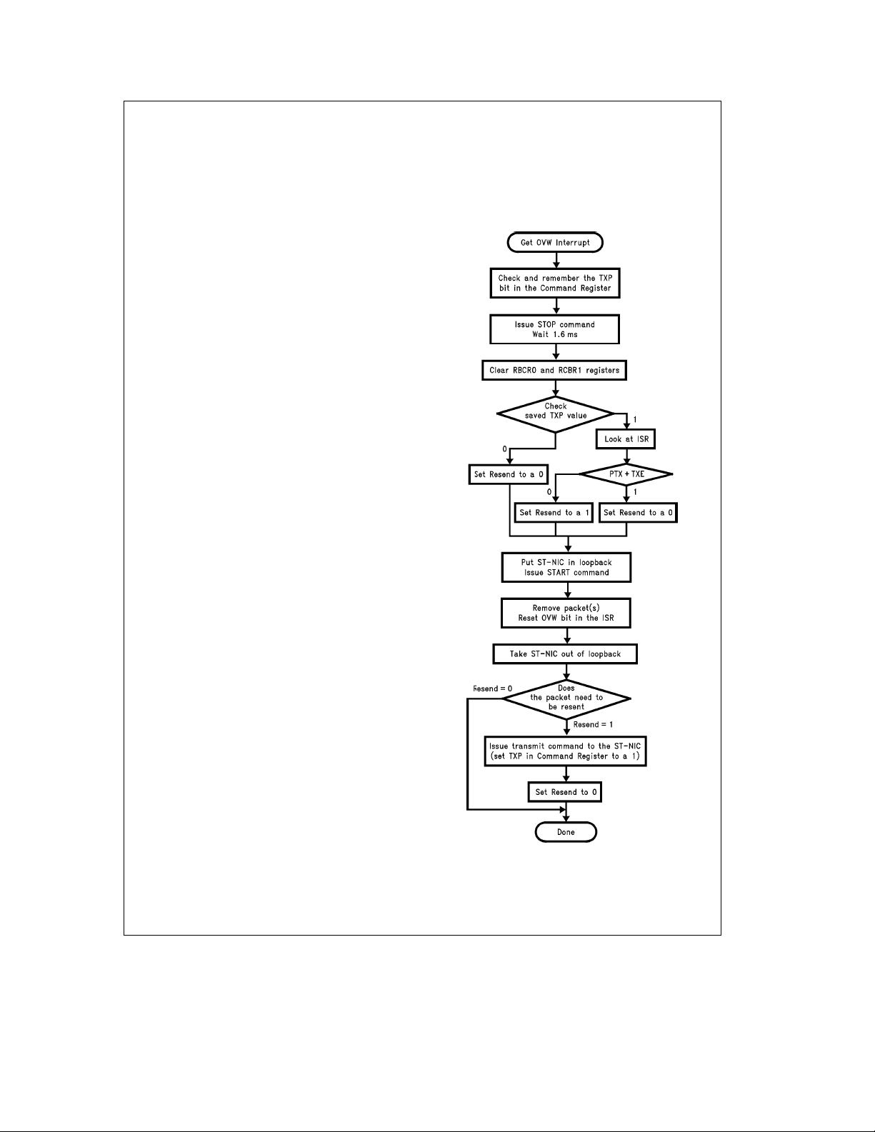
In heavily loaded network which cause overflows of the Receive Buffer Ring, the ST-NIC may disable the local DMA
and suspend further receptions even if the Boundary register is advanced beyond the Current register. To guarantee
this will not happen, a software reset must be issued during
all Receive Buffer Ring overflows (indicated by the OVW bit
in the Interrupt Status Register). The following procedure is
required to recover from a Receiver Buffer Ring Overflow.
If this routine is not adhered to, the ST-NIC may act in an
unpredictable manner. It should also be noted that it is not
permissible to service an overflow interrupt by continuing to
empty packets from the receive buffer without implementing
the prescribed overflow routine. A flow chart of the ST-NIC’s
overflow routine follows.
Note: It is necessary to define a variable in the driver, which will be called
‘‘Resend’’.
1. Read and store the value of the TXP bit in the ST-NIC
Command Register.
2. Issue the STOP command to the ST-NIC. This is accomplished by setting the STP bit in the ST-NIC’s Command
Register. Writing 21H to the Command Register will stop
the ST-NIC.
3. Wait for at least 1.6 ms. Since the ST-NIC will complete
any transmission or reception that is in progress, it is
necessary to time out for the maximum possible duration
of an Ethernet transmission or reception. By waiting
1.6 ms this is achieved with some guard band added.
Previously, it was recommended that the RST bit of the
Interrupt Status Register be polled to insure that the
pending transmission or reception is completed. This bit
is not a reliable indicator and subsequently should be
ignored.
4. Clear the ST-NIC’s Remote Byte Count registers
(RBCR0 and RBCR1).
5. Read the stored value of the TXP bit from step 1, above.
If this value is a 0, set the ‘‘Resend’’ variable to a 0 and
jump to step 6.
If this value is a 1, read the ST-NIC’s Interrupt Status
Register. If either the Packet Transmitted bit (PTX) or
Transmit Error bit (TXE) is set to a 1, set the ‘‘Resend’’
variable to a 0 and jump to step 6. If neither of these bits
is set, placea1inthe‘‘Resend’’ variable and jump to
step 6.
This step determines if there was a transmission in progress when the stop command was issued in step 2. If
there was a transmission in progress, the ST-NIC’s ISR
is read to determine whether or not the packet was recognized by the ST-NIC. If neither the PTX nor TXE bit
was set, then the packet will essentially be lost and retransmitted only after a time-out takes place in the upper
level software. By determining that the packet was lost at
the driver level, a transmit command can be reissued to
the ST-NIC once the overflow routine is completed (as in
step 11). Also, it is possible for the ST-NIC to defer indefinitely, when it is stopped on a busy network. Step 5 also
alleviates this problem. Step 5 is essential and should
not be omitted from the overflow routine, in order for the
ST-NIC to operate correctly.
Overflow Routine Flow Chart
TL/F/11157– 57
17
7.0 Packet Reception (Continued)
6. Place the ST-NIC in either mode 1 or mode 2 loopback.
This can be accomplished by setting bits D2 and D1, of
the Transmit Configuration Register, to ‘‘0,1’’ or ‘‘1,0’’,
respectively.
7. Issue the START command to the ST-NIC. This can be
accomplished by writing 22H to the Command Register.
This is necessary to activate the ST-NIC’s Remote DMA
channel.
8. Remove one or more packets from the receive buffer
ring.
9. Reset the overwrite warning (OVW, overflow) bit in the
Interrupt Status Register.
Received Packet Aborted If It Hits Boundary
10. Take the ST-NIC out of loopback. This is done by writing the Transmit Configration Register with the value it
contains during normal operation. (Bits D2 and D1
should both be programmed to 0.)
11. If the ‘‘Resend’’ variable is set to a 1, reset the ‘‘Resend’’ variable and reissue the transmit command. This
is done by writing a value of 26H to the Command Register. If the ‘‘Resend’’ variable is 0, nothing needs to be
done.
Note 1: If Remote DMA is not being used, the ST-NIC does not need to be
started before packets can be removed from the receive buffer ring. Hence,
step 8 could be done before step 7.
Note 2: When the ST-NIC is in STOP mode, the Missed Talley Counter is
disabled
TL/F/11157– 13
18
7.0 Packet Reception (Continued)
Enabling the ST-NIC On An Active Network
After the ST-NIC has been initialized the procedure for disabling and then re-enabling the ST-NIC on the network is
similar to handling Receive Buffer Ring overflow as described previously.
1. Program Command Register for page 0 (Command Reg-
e
ister
21H)
2. Initialize Data Configuration Register (DCR)
3. Clear Remote Byte Count Registers (RBCR0, RBCR1)
4. Initialize Receive Configuration Register (RCR)
5. Place the ST-NIC in LOOPBACK mode 1 or 2 (Transmit
Configuration Register
6. Initialize Receive Buffer Ring: Boundary Pointer
(BNDRY), Page Start (PSTART), and Page Stop
(PSTOP)
7. Clear Interrupt Status Register (ISR) by writing 0FFH to
it.
8. Initialize Interrupt Mask Register (IMR)
9. Program Command Register for page 1 (Command Reg-
e
ister
61H)
i. Initialize Physical Address Registers (PAR0–PAR5)
ii. Initialize Multicast Address Registers (MAR0 – MAR7)
iii. Initialize CURRent pointer
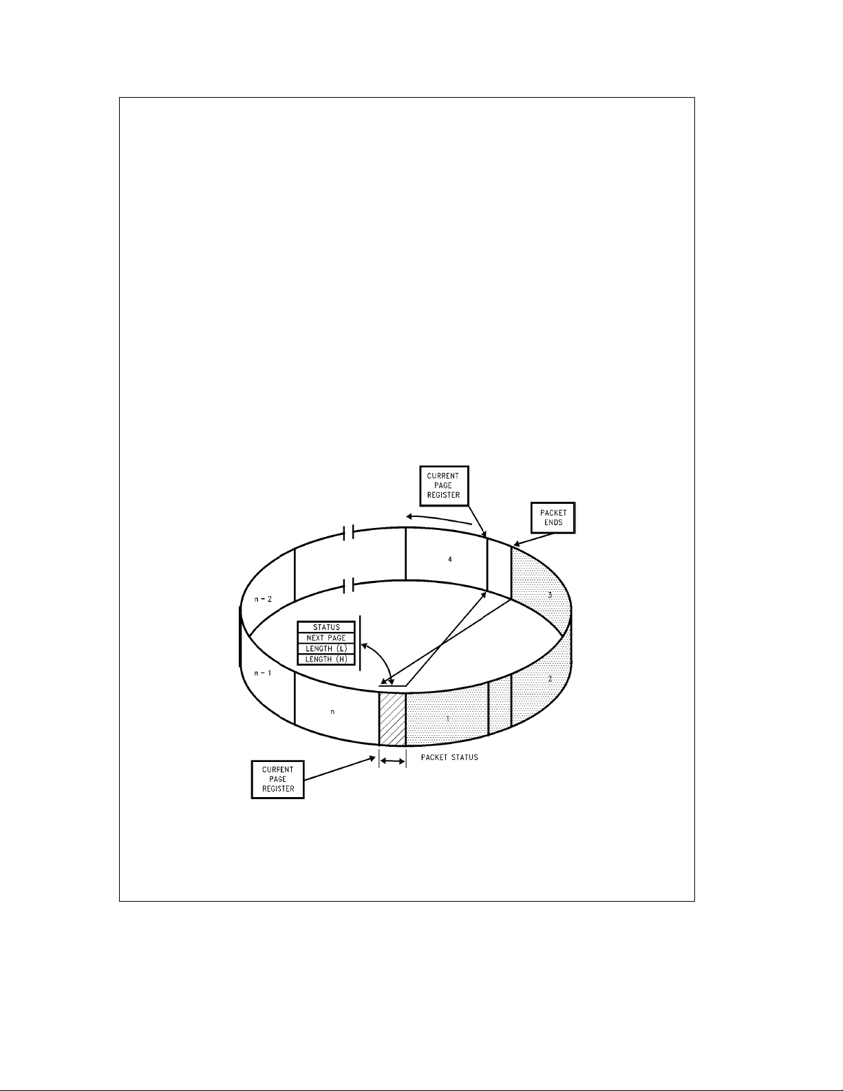
e
02H or 04H)
Termination of Received PacketÐPacket Accepted
10. Put ST-NIC in START mode (Command Register
22H). The local receive DMA is still not active since the
ST-NIC is in LOOPBACK.
11. Initialize the Transmit Configuration for the intended
value. The ST-NIC is now ready for transmission and
reception.
END OF PACKET OPERATIONS
At the end of the packet the ST-NIC determines whether the
received packet is to be accepted or rejected. It either
branches to a routine to store the Buffer Header or to another routine that recovers the buffers used to store the packet.
SUCCESSFUL RECEPTION
If the packet is successfully received, the DMA is restored
to the first buffer used to store the packet (pointed to by the
Current Page Register). The DMA then stores the Receive
Status, a Pointer to where the next packet will be stored
(Buffer 4) and the number of received bytes. Note that the
remaining bytes in the last buffer are discarded and reception of the next packet begins on the next empty 256-byte
buffer boundary. The Current Page Register is then initialized to the next available buffer in the Buffer Ring. (The
location of the next buffer had been previously calculated
and temporarily stored in an internal scratchpad register.)
e
TL/F/11157– 14
19
7.0 Packet Reception (Continued)
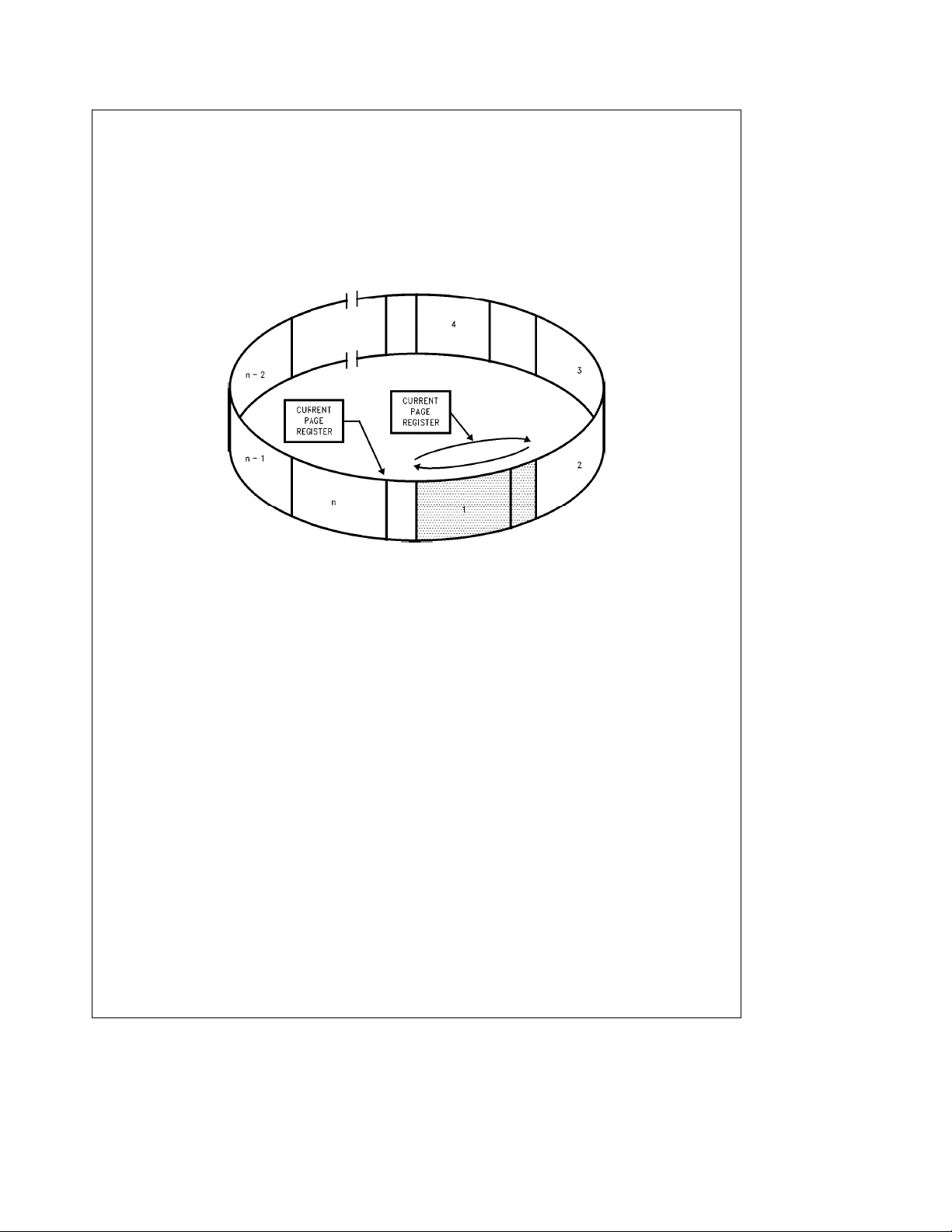
BUFFER RECOVERY FOR REJECTED PACKETS
If the packet is a runt packet or contains CRC or Frame
Alignment errors, it is rejected. The buffer management logic resets the DMA back to the first buffer page used to store
the packet (pointed to by CURR), recovering all buffers that
had been used to store the rejected packet. This operation
will not be performed if the ST-NIC is programmed to accept
either runt packets or packets with CRC or Frame Alignment
Termination of Receive PacketÐPacket Reject
errors. The received CRC is always stored in buffer memory
after the last byte of received data for the packet.
Error Recovery
If the packet is rejected as shown, the DMA is restored by
the ST-NIC by reprogramming the DMA starting address
pointed to by the Current Page Register.
TL/F/11157– 15
20
7.0 Packet Reception (Continued)
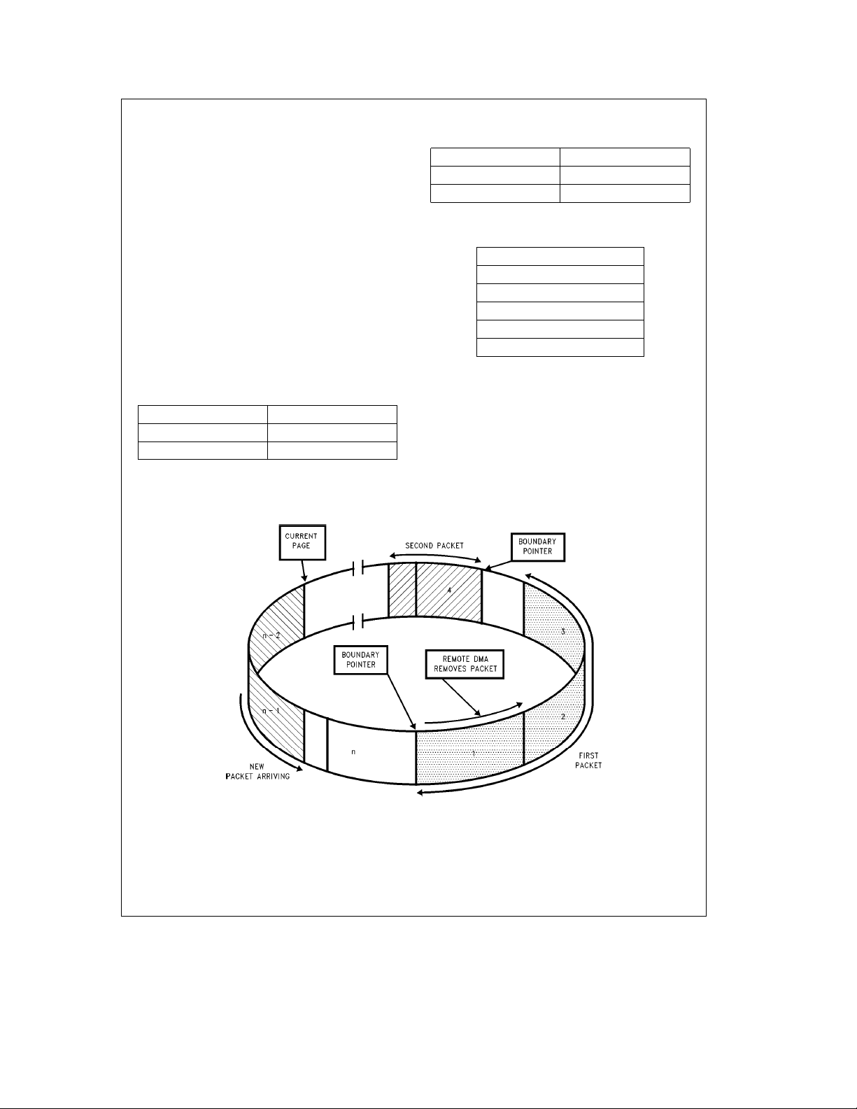
REMOVING PACKETS FROM THE RING
Packets are removed from the ring using the Remote DMA
or an external device. When using the Remote DMA the
Send Packet command can be used. This programs the Remote DMA to automatically remove the received packet
pointed to by the Boundary Pointer. At the end of the transfer, the ST-NIC moves the Boundary Pointer, freeing additional buffers for reception. The Boundary Pointer can also
be moved manually by programming the Boundary Register.
The ST-NIC knows the difference between an empty buffer
ring and a full buffer ring. This situation is seen when the
Boundary Pointer (BNDRY) and the Current Page Pointer
(CURR) point to the same address. If BNDRY caught up
with CURR the buffer is empty and if CURR caught up with
BNDRY the buffer is full.
STORAGE FORMAT FOR RECEIVED PACKETS
The following diagrams describe the format for how received packets are placed into memory by the local DMA
channel. These modes are selected in the Data Configuration Register.
AD15 AD8 AD7 AD0
Next Packet Pointer Receive Status
Receive Byte Count 1 Receive Byte Count 0
Byte 2 Byte 1
BOSe0, WTSe1 in Data Configuration Register. This format is used with
Series 32xxx, or 680x0 processors.
1st Received Packet Removed by Remote DMA
AD15 AD8 AD7 AD0
Next Packet Pointer Receive Status
Receive Byte Count 0 Receive Byte Count 1
Byte 1 Byte 2
BOSe1, WTSe1 in Data Configuration Register. This format is used with
680x0 type processors. (Note: The Receive Count ordering remains the
same for BOS
e
0or1.)
Receive Status
Next Packet Pointer
Receive Byte Count 0
Receive Byte Count 1
Byte 0
Byte 1
BOSe0, WTSe0 in Data Configuration Register. This format is used with
general 8-bit processors.
TL/F/11157– 16
21
 Loading...