

© 2006 National Semiconductor Corporation www.national.com
1
DP83849I PHYTER® DUAL Industrial Temperature with Flexible Port Switching
Dual Port 10/100 Mb/s Ethernet Physical Layer Transceiver
August 2006
DP83849I PHYTER® DUAL Industrial Temperature with Flexible Port Switching
Dual Port 10/100 Mb/s Ethernet Physical Layer Transceiver
General Description
The number of applications requiring Ethernet Connectivity continues to expand. Along with this
increased market demand is a change in application
requirements. Where single channel Ethernet used to
be sufficient, many applications such as wireless
remote base stations and industrial networking now
require DUAL Port functionality for redundancy or system management.
The DP83849I is a highly reliable, feature rich device
perfectly suited for industrial applications enabling
Ethernet on the factory floor. The DP83849I features
two fully independent 10/100 ports for multi-port applications. NATIONAL’s unique port switching capability
also allows the two ports to be configured to provide
fully integrated range extension, media conversion,
hardware based failover and port monitoring.
The DP83849I provides optimum flexibility in MPU
selection by supporting both MII and RMII interfaces.
In additio n this device includes a powerful new diagnostics tool to ensure initial network operation and
maintenance.
In addition to the TDR scheme, commonly used for
detecting faults during installation, NATIONAL’s innovative cable diagnostics provides for real time continuous monitoring of the link quality. This allows the
system designer to implement a fault prediction mechanism to detect and warn of changing or deteriorating
link conditions.
With the DP83849I, National Semiconductor continues
to build on its Ethernet expertise and leadership position by providing a powerful combination of features
and flexibility, easing Ethernet implementation for the
system designer.
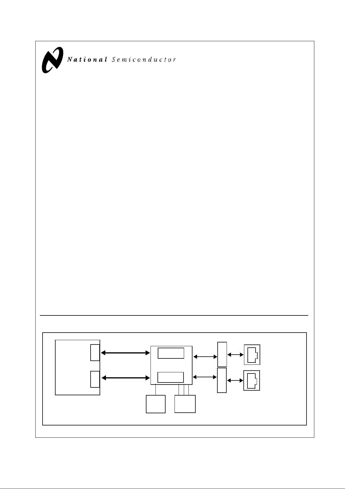
System Diagram
PHYTER is a registered trademark of National Semiconductor Corporation
Status
10BASE-T
or
100BASE-TX
MII/RMII/SNI
25 MHz
Magnetics
RJ-45
Clock
LEDs
DP83849I
MPU/CPU
Source
Typical Application
MAC
MAC
MII/RMII/SNI
10BASE-T
or
100BASE-TX
Magnetics
RJ-45
Port A
Port B
Features
• Low-power 3.3V, 0.18µm CMOS technology
• Low power consumption <600mW Typical
• 3.3V MAC Interface
• Auto-MDIX for 10/100 Mb/s
• Energy Detection Mode
• Flexible MII Port Assignment
• Dynamic Integrity Utility
• Dynamic Link Quality Monitoring
• TDR based Cable Diagnostic and Cable Length Detection
• Optimized Latency for Real Time Ethernet Operation
• Reference Clock out
• RMII Rev. 1.2 Interface (configurable)
• SNI Interface (configurable)
• MII Serial Management Interface (MDC and MDIO)
• IEEE 802.3u MII
• IEEE 802.3u Auto-Negotiation and Parallel Detection
• IEEE 802.3u ENDEC, 10BASE-T transceivers and filters
• IEEE 802.3u PCS, 100BASE-TX transceivers and filters
• IEEE 1149.1 JTAG
• Integrated ANSI X3.263 compliant TP-PMD physical sub-layer
with adaptive equalization and Baseline Wander compensation
• Programmable LED support for Link, 10 /100 Mb/s Mode, Activ-
ity, Duplex and Collision Detect
• Single register access for complete PHY status
• 10/100 Mb/s packet BIST (Built in Self Test)
• 80-pin TQFP package (12mm x 12mm)
Applications
• Medical Instrumentation
• Factory Automation
• Motor & Motion Control
• Wireless Remote Base Station
• General Embedded Applications
2 www.national.com
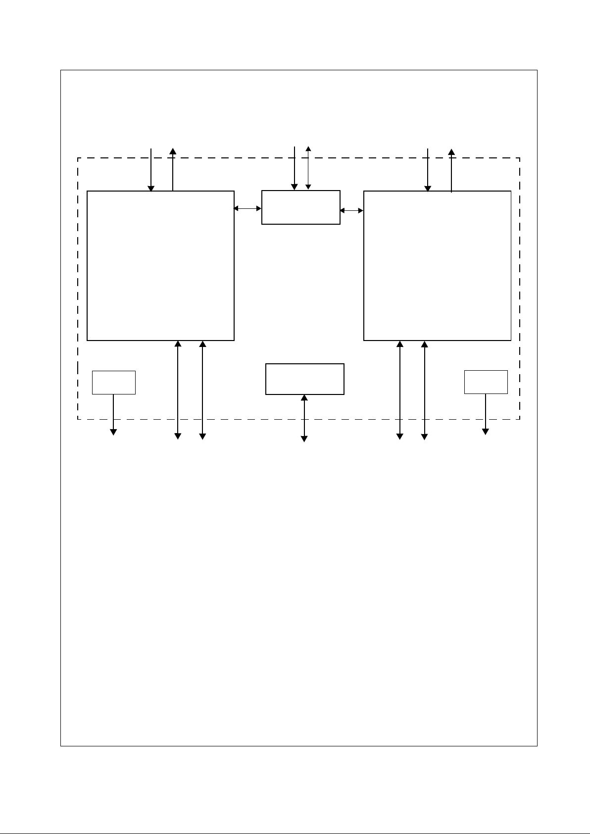
DP83849I
MANAGEMENT
RXTXTX RX
LED
DRIVERS
LEDS
INTERFACE
10/100 PHY CORE
10/100 PHY CORE
BOUNDARY
JTAG
SCAN
MII/RMII/SNI
PORT A
MII/RMII/SNI
PORT B
MII MANAGEMENT
INTERFACE
MDC
MDIO
LED
DRIVERS
LEDS
PORT B
PORT A
TPTD±
TPRD±
TPTD±
TPRD±
Figure 1. DP83849I Functional Block Diagram

3 www.national.com
DP83849I
Table of Contents
1.0 Pin Descriptions . . . . . . . . . . . . . . . . . . . . . . . . . . . . . . . . . . . . . . . . . . . . . . . . 10
1.1 Serial Management Interface . . . . . . . . . . . . . . . . . . . . . . . . . . . . . . . . . . . . . . . . . . . . . .10
1.2 MAC Data Interface . . . . . . . . . . . . . . . . . . . . . . . . . . . . . . . . . . . . . . . . . . . . . . . . . . . . .10
1.3 Clock Interface . . . . . . . . . . . . . . . . . . . . . . . . . . . . . . . . . . . . . . . . . . . . . . . . . . . . . . . . .12
1.4 LED Interface . . . . . . . . . . . . . . . . . . . . . . . . . . . . . . . . . . . . . . . . . . . . . . . . . . . . . . . . . .12
1.5 JTAG Interface . . . . . . . . . . . . . . . . . . . . . . . . . . . . . . . . . . . . . . . . . . . . . . . . . . . . . . . . .13
1.6 Reset and Power Down . . . . . . . . . . . . . . . . . . . . . . . . . . . . . . . . . . . . . . . . . . . . . . . . . .13
1.7 Strap Options . . . . . . . . . . . . . . . . . . . . . . . . . . . . . . . . . . . . . . . . . . . . . . . . . . . . . . . . . .13
1.8 10 Mb/s and 100 Mb/s PMD Interface . . . . . . . . . . . . . . . . . . . . . . . . . . . . . . . . . . . . . . .16
1.9 Special Connections . . . . . . . . . . . . . . . . . . . . . . . . . . . . . . . . . . . . . . . . . . . . . . . . . . . . .16
1.10 Power Supply Pins . . . . . . . . . . . . . . . . . . . . . . . . . . . . . . . . . . . . . . . . . . . . . . . . . . . . .16
1.11 Package Pin Assignments . . . . . . . . . . . . . . . . . . . . . . . . . . . . . . . . . . . . . . . . . . . . . . .17
2.0 Configuration . . . . . . . . . . . . . . . . . . . . . . . . . . . . . . . . . . . . . . . . . . . . . . . . . . 18
2.1 Auto-Negotiation . . . . . . . . . . . . . . . . . . . . . . . . . . . . . . . . . . . . . . . . . . . . . . . . . . . . . . . .18
2.1.1 Auto-Negotiation Pin Control . . . . . . . . . . . . . . . . . . . . . . . . . . . . . . . . . . . . . . . . . . . . . . . . . 18
2.1.2 Auto-Negotiation Register Control . . . . . . . . . . . . . . . . . . . . . . . . . . . . . . . . . . . . . . . . . . . . . 18
2.1.3 Auto-Negotiation Parallel Detection . . . . . . . . . . . . . . . . . . . . . . . . . . . . . . . . . . . . . . . . . . . . 19
2.1.4 Auto-Negotiation Restart . . . . . . . . . . . . . . . . . . . . . . . . . . . . . . . . . . . . . . . . . . . . . . . . . . . . 19
2.1.5 Enabling Auto-Negotiation via Software . . . . . . . . . . . . . . . . . . . . . . . . . . . . . . . . . . . . . . . . 19
2.1.6 Auto-Negotiation Complete Time . . . . . . . . . . . . . . . . . . . . . . . . . . . . . . . . . . . . . . . . . . . . . . 19
2.2 Auto-MDIX . . . . . . . . . . . . . . . . . . . . . . . . . . . . . . . . . . . . . . . . . . . . . . . . . . . . . . . . . . . .19
2.3 PHY Address . . . . . . . . . . . . . . . . . . . . . . . . . . . . . . . . . . . . . . . . . . . . . . . . . . . . . . . . . .19
2.3.1 MII Isolate Mode . . . . . . . . . . . . . . . . . . . . . . . . . . . . . . . . . . . . . . . . . . . . . . . . . . . . . . . . . . 20
2.4 LED Interface . . . . . . . . . . . . . . . . . . . . . . . . . . . . . . . . . . . . . . . . . . . . . . . . . . . . . . . . . .21
2.4.1 LEDs . . . . . . . . . . . . . . . . . . . . . . . . . . . . . . . . . . . . . . . . . . . . . . . . . . . . . . . . . . . . . . . . . . . 21
2.4.2 LED Direct Control . . . . . . . . . . . . . . . . . . . . . . . . . . . . . . . . . . . . . . . . . . . . . . . . . . . . . . . . . 22
2.5 Half Duplex vs. Full Duplex . . . . . . . . . . . . . . . . . . . . . . . . . . . . . . . . . . . . . . . . . . . . . . .22
2.6 Internal Loopback . . . . . . . . . . . . . . . . . . . . . . . . . . . . . . . . . . . . . . . . . . . . . . . . . . . . . . .22
2.7 BIST . . . . . . . . . . . . . . . . . . . . . . . . . . . . . . . . . . . . . . . . . . . . . . . . . . . . . . . . . . . . . . . . .22
3.0 MAC Interface . . . . . . . . . . . . . . . . . . . . . . . . . . . . . . . . . . . . . . . . . . . . . . . . . . 23
3.1 MII Interface . . . . . . . . . . . . . . . . . . . . . . . . . . . . . . . . . . . . . . . . . . . . . . . . . . . . . . . . . . .23
3.1.1 Nibble-wide MII Data Interface . . . . . . . . . . . . . . . . . . . . . . . . . . . . . . . . . . . . . . . . . . . . . . . . 23
3.1.2 Collision Detect . . . . . . . . . . . . . . . . . . . . . . . . . . . . . . . . . . . . . . . . . . . . . . . . . . . . . . . . . . . 23
3.1.3 Carrier Sense . . . . . . . . . . . . . . . . . . . . . . . . . . . . . . . . . . . . . . . . . . . . . . . . . . . . . . . . . . . . . 23
3.2 Reduced MII Interface . . . . . . . . . . . . . . . . . . . . . . . . . . . . . . . . . . . . . . . . . . . . . . . . . . .24
3.3 10 Mb Serial Network Interface (SNI) . . . . . . . . . . . . . . . . . . . . . . . . . . . . . . . . . . . . . . . .25
3.4 Single Clock MII Mode . . . . . . . . . . . . . . . . . . . . . . . . . . . . . . . . . . . . . . . . . . . . . . . . . . .25
3.5 Flexible MII Port Assignment . . . . . . . . . . . . . . . . . . . . . . . . . . . . . . . . . . . . . . . . . . . . . .26
3.5.1 RX MII Port Mapping . . . . . . . . . . . . . . . . . . . . . . . . . . . . . . . . . . . . . . . . . . . . . . . . . . . . . . . 27
3.5.2 TX MII Port Mapping . . . . . . . . . . . . . . . . . . . . . . . . . . . . . . . . . . . . . . . . . . . . . . . . . . . . . . . 28
3.5.3 Common Flexible MII Port Configurations . . . . . . . . . . . . . . . . . . . . . . . . . . . . . . . . . . . . . . . 28
3.5.4 Strapped Extender Mode . . . . . . . . . . . . . . . . . . . . . . . . . . . . . . . . . . . . . . . . . . . . . . . . . . . . 29
3.5.5 Notes and Restrictions . . . . . . . . . . . . . . . . . . . . . . . . . . . . . . . . . . . . . . . . . . . . . . . . . . . . . . 29
3.6 802.3u MII Serial Management Interface . . . . . . . . . . . . . . . . . . . . . . . . . . . . . . . . . . . . .30
3.6.1 Serial Management Register Access . . . . . . . . . . . . . . . . . . . . . . . . . . . . . . . . . . . . . . . . . . . 30
3.6.2 Serial Management Access Protocol . . . . . . . . . . . . . . . . . . . . . . . . . . . . . . . . . . . . . . . . . . . 30
3.6.3 Serial Management Preamble Suppression . . . . . . . . . . . . . . . . . . . . . . . . . . . . . . . . . . . . . 31
3.6.4 Simultaneous Register Write . . . . . . . . . . . . . . . . . . . . . . . . . . . . . . . . . . . . . . . . . . . . . . . . . 31
4.0 Architecture. . . . . . . . . . . . . . . . . . . . . . . . . . . . . . . . . . . . . . . . . . . . . . . . . . . . 32
4.1 100BASE-TX TRANSMITTER . . . . . . . . . . . . . . . . . . . . . . . . . . . . . . . . . . . . . . . . . . . . .32
4.1.1 Code-group Encoding and Injection . . . . . . . . . . . . . . . . . . . . . . . . . . . . . . . . . . . . . . . . . . . . 34
4.1.2 Scrambler . . . . . . . . . . . . . . . . . . . . . . . . . . . . . . . . . . . . . . . . . . . . . . . . . . . . . . . . . . . . . . . . 34
4.1.3 NRZ to NRZI Encoder . . . . . . . . . . . . . . . . . . . . . . . . . . . . . . . . . . . . . . . . . . . . . . . . . . . . . . 34
4.1.4 Binary to MLT-3 Convertor . . . . . . . . . . . . . . . . . . . . . . . . . . . . . . . . . . . . . . . . . . . . . . . . . . . 34

4 www.national.com
DP83849I
4.2 100BASE-TX RECEIVER . . . . . . . . . . . . . . . . . . . . . . . . . . . . . . . . . . . . . . . . . . . . . . . . .34
4.2.1 Analog Front End . . . . . . . . . . . . . . . . . . . . . . . . . . . . . . . . . . . . . . . . . . . . . . . . . . . . . . . . . . 34
4.2.2 Digital Signal Processor . . . . . . . . . . . . . . . . . . . . . . . . . . . . . . . . . . . . . . . . . . . . . . . . . . . . . 34
4.2.2.1 Digital Adaptive Equalization and Gain Control . . . . . . . . . . . . . . . . . . . . . . . . . . . . . . 36
4.2.2.2 Base Line Wander Compensation . . . . . . . . . . . . . . . . . . . . . . . . . . . . . . . . . . . . . . . . 37
4.2.3 Signal Detect . . . . . . . . . . . . . . . . . . . . . . . . . . . . . . . . . . . . . . . . . . . . . . . . . . . . . . . . . . . . . 37
4.2.4 MLT-3 to NRZI Decoder . . . . . . . . . . . . . . . . . . . . . . . . . . . . . . . . . . . . . . . . . . . . . . . . . . . . . 37
4.2.5 NRZI to NRZ . . . . . . . . . . . . . . . . . . . . . . . . . . . . . . . . . . . . . . . . . . . . . . . . . . . . . . . . . . . . . 37
4.2.6 Serial to Parallel . . . . . . . . . . . . . . . . . . . . . . . . . . . . . . . . . . . . . . . . . . . . . . . . . . . . . . . . . . . 37
4.2.7 Descrambler . . . . . . . . . . . . . . . . . . . . . . . . . . . . . . . . . . . . . . . . . . . . . . . . . . . . . . . . . . . . . . 38
4.2.8 Code-group Alignment . . . . . . . . . . . . . . . . . . . . . . . . . . . . . . . . . . . . . . . . . . . . . . . . . . . . . . 38
4.2.9 4B/5B Decoder . . . . . . . . . . . . . . . . . . . . . . . . . . . . . . . . . . . . . . . . . . . . . . . . . . . . . . . . . . . . 38
4.2.10 100BASE-TX Link Integrity Monitor . . . . . . . . . . . . . . . . . . . . . . . . . . . . . . . . . . . . . . . . . . . 38
4.2.11 Bad SSD Detection . . . . . . . . . . . . . . . . . . . . . . . . . . . . . . . . . . . . . . . . . . . . . . . . . . . . . . . 38
4.3 10BASE-T TRANSCEIVER MODULE . . . . . . . . . . . . . . . . . . . . . . . . . . . . . . . . . . . . . . .38
4.3.1 Operational Modes . . . . . . . . . . . . . . . . . . . . . . . . . . . . . . . . . . . . . . . . . . . . . . . . . . . . . . . . . 38
4.3.2 Smart Squelch . . . . . . . . . . . . . . . . . . . . . . . . . . . . . . . . . . . . . . . . . . . . . . . . . . . . . . . . . . . . 38
4.3.3 Collision Detection and SQE . . . . . . . . . . . . . . . . . . . . . . . . . . . . . . . . . . . . . . . . . . . . . . . . . 40
4.3.4 Carrier Sense . . . . . . . . . . . . . . . . . . . . . . . . . . . . . . . . . . . . . . . . . . . . . . . . . . . . . . . . . . . . . 40
4.3.5 Normal Link Pulse Detection/Generation . . . . . . . . . . . . . . . . . . . . . . . . . . . . . . . . . . . . . . . . 40
4.3.6 Jabber Function . . . . . . . . . . . . . . . . . . . . . . . . . . . . . . . . . . . . . . . . . . . . . . . . . . . . . . . . . . . 40
4.3.7 Automatic Link Polarity Detection and Correction . . . . . . . . . . . . . . . . . . . . . . . . . . . . . . . . . 40
4.3.8 Transmit and Receive Filtering . . . . . . . . . . . . . . . . . . . . . . . . . . . . . . . . . . . . . . . . . . . . . . . 40
4.3.9 Transmitter . . . . . . . . . . . . . . . . . . . . . . . . . . . . . . . . . . . . . . . . . . . . . . . . . . . . . . . . . . . . . . . 40
4.3.10 Receiver . . . . . . . . . . . . . . . . . . . . . . . . . . . . . . . . . . . . . . . . . . . . . . . . . . . . . . . . . . . . . . . . 40
5.0 Design Guidelines. . . . . . . . . . . . . . . . . . . . . . . . . . . . . . . . . . . . . . . . . . . . . . . 41
5.1 TPI Network Circuit . . . . . . . . . . . . . . . . . . . . . . . . . . . . . . . . . . . . . . . . . . . . . . . . . . . . . .41
5.2 ESD Protection . . . . . . . . . . . . . . . . . . . . . . . . . . . . . . . . . . . . . . . . . . . . . . . . . . . . . . . . .42
5.3 Clock In (X1) Requirements . . . . . . . . . . . . . . . . . . . . . . . . . . . . . . . . . . . . . . . . . . . . . . .42
5.4 Power Feedback Circuit . . . . . . . . . . . . . . . . . . . . . . . . . . . . . . . . . . . . . . . . . . . . . . . . . .43
5.5 Power Down/Interrupt . . . . . . . . . . . . . . . . . . . . . . . . . . . . . . . . . . . . . . . . . . . . . . . . . . . .43
5.5.1 Power Down Control Mode . . . . . . . . . . . . . . . . . . . . . . . . . . . . . . . . . . . . . . . . . . . . . . . . . . 43
5.5.2 Interrupt Mechanisms . . . . . . . . . . . . . . . . . . . . . . . . . . . . . . . . . . . . . . . . . . . . . . . . . . . . . . 44
5.6 Energy Detect Mode . . . . . . . . . . . . . . . . . . . . . . . . . . . . . . . . . . . . . . . . . . . . . . . . . . . . .44
5.7 Link Diagnostic Capabilities . . . . . . . . . . . . . . . . . . . . . . . . . . . . . . . . . . . . . . . . . . . . . . .44
5.7.1 Linked Cable Status . . . . . . . . . . . . . . . . . . . . . . . . . . . . . . . . . . . . . . . . . . . . . . . . . . . . . . . . 44
5.7.1.1 Polarity Reversal . . . . . . . . . . . . . . . . . . . . . . . . . . . . . . . . . . . . . . . . . . . . . . . . . . . . . 44
5.7.1.2 Cable Swap Indication . . . . . . . . . . . . . . . . . . . . . . . . . . . . . . . . . . . . . . . . . . . . . . . . . 44
5.7.1.3 100MB Cable Length Estimation . . . . . . . . . . . . . . . . . . . . . . . . . . . . . . . . . . . . . . . . . 44
5.7.1.4 Frequency Offset Relative to Link Partner . . . . . . . . . . . . . . . . . . . . . . . . . . . . . . . . . . 44
5.7.1.5 Cable Signal Quality Estimation . . . . . . . . . . . . . . . . . . . . . . . . . . . . . . . . . . . . . . . . . 45
5.7.2 Link Quality Monitor . . . . . . . . . . . . . . . . . . . . . . . . . . . . . . . . . . . . . . . . . . . . . . . . . . . . . . . . 45
5.7.2.1 Link Quality Monitor Control and Status . . . . . . . . . . . . . . . . . . . . . . . . . . . . . . . . . . . 45
5.7.2.2 Checking Current Parameter Values . . . . . . . . . . . . . . . . . . . . . . . . . . . . . . . . . . . . . . 45
5.7.2.3 Threshold Control . . . . . . . . . . . . . . . . . . . . . . . . . . . . . . . . . . . . . . . . . . . . . . . . . . . . 45
5.7.3 TDR Cable Diagnostics . . . . . . . . . . . . . . . . . . . . . . . . . . . . . . . . . . . . . . . . . . . . . . . . . . . . . 46
5.7.3.1 TDR Pulse Generator . . . . . . . . . . . . . . . . . . . . . . . . . . . . . . . . . . . . . . . . . . . . . . . . . 46
5.7.3.2 TDR Pulse Monitor . . . . . . . . . . . . . . . . . . . . . . . . . . . . . . . . . . . . . . . . . . . . . . . . . . . 46
5.7.3.3 TDR Control Interface . . . . . . . . . . . . . . . . . . . . . . . . . . . . . . . . . . . . . . . . . . . . . . . . . 46
5.7.3.4 TDR Results . . . . . . . . . . . . . . . . . . . . . . . . . . . . . . . . . . . . . . . . . . . . . . . . . . . . . . . . 47
6.0 Reset Operation . . . . . . . . . . . . . . . . . . . . . . . . . . . . . . . . . . . . . . . . . . . . . . . . 48
6.1 Hardware Reset . . . . . . . . . . . . . . . . . . . . . . . . . . . . . . . . . . . . . . . . . . . . . . . . . . . . . . . .48
6.2 Full Software Reset . . . . . . . . . . . . . . . . . . . . . . . . . . . . . . . . . . . . . . . . . . . . . . . . . . . . .48
6.3 Soft Reset . . . . . . . . . . . . . . . . . . . . . . . . . . . . . . . . . . . . . . . . . . . . . . . . . . . . . . . . . . . . .48
7.0 Register Block . . . . . . . . . . . . . . . . . . . . . . . . . . . . . . . . . . . . . . . . . . . . . . . . . 49
7.1 Register Definition . . . . . . . . . . . . . . . . . . . . . . . . . . . . . . . . . . . . . . . . . . . . . . . . . . . . . .53
7.1.1 Basic Mode Control Register (BMCR) . . . . . . . . . . . . . . . . . . . . . . . . . . . . . . . . . . . . . . . . . . 54
7.1.2 Basic Mode Status Register (BMSR) . . . . . . . . . . . . . . . . . . . . . . . . . . . . . . . . . . . . . . . . . . . 56
7.1.3 PHY Identifier Register #1 (PHYIDR1) . . . . . . . . . . . . . . . . . . . . . . . . . . . . . . . . . . . . . . . . . . 57
7.1.4 PHY Identifier Register #2 (PHYIDR2) . . . . . . . . . . . . . . . . . . . . . . . . . . . . . . . . . . . . . . . . . . 57

5 www.national.com
DP83849I
7.1.5 Auto-Negotiation Advertisement Register (ANAR) . . . . . . . . . . . . . . . . . . . . . . . . . . . . . . . . . 57
7.1.6 Auto-Negotiation Link Partner Ability Register (ANLPAR) (BASE Page) . . . . . . . . . . . . . . . . 59
7.1.7 Auto-Negotiation Link Partner Ability Register (ANLPAR) (Next Page) . . . . . . . . . . . . . . . . . 60
7.1.8 Auto-Negotiate Expansion Register (ANER) . . . . . . . . . . . . . . . . . . . . . . . . . . . . . . . . . . . . . 61
7.1.9 Auto-Negotiation Next Page Transmit Register (ANNPTR) . . . . . . . . . . . . . . . . . . . . . . . . . . 62
7.1.10 PHY Status Register (PHYSTS) . . . . . . . . . . . . . . . . . . . . . . . . . . . . . . . . . . . . . . . . . . . . . 63
7.1.11 MII Interrupt Control Register (MICR) . . . . . . . . . . . . . . . . . . . . . . . . . . . . . . . . . . . . . . . . . 65
7.1.12 MII Interrupt Status and Misc. Control Register (MISR) . . . . . . . . . . . . . . . . . . . . . . . . . . . . 65
7.1.13 Page Select Register (PAGESEL) . . . . . . . . . . . . . . . . . . . . . . . . . . . . . . . . . . . . . . . . . . . . 66
7.2 Extended Registers - Page 0 . . . . . . . . . . . . . . . . . . . . . . . . . . . . . . . . . . . . . . . . . . . . . .67
7.2.1 False Carrier Sense Counter Register (FCSCR) . . . . . . . . . . . . . . . . . . . . . . . . . . . . . . . . . . 67
7.2.2 Receiver Error Counter Register (RECR) . . . . . . . . . . . . . . . . . . . . . . . . . . . . . . . . . . . . . . . 67
7.2.3 100 Mb/s PCS Configuration and Status Register (PCSR) . . . . . . . . . . . . . . . . . . . . . . . . . . 67
7.2.4 RMII and Bypass Register (RBR) . . . . . . . . . . . . . . . . . . . . . . . . . . . . . . . . . . . . . . . . . . . . . 69
7.2.5 LED Direct Control Register (LEDCR) . . . . . . . . . . . . . . . . . . . . . . . . . . . . . . . . . . . . . . . . . . 71
7.2.6 PHY Control Register (PHYCR) . . . . . . . . . . . . . . . . . . . . . . . . . . . . . . . . . . . . . . . . . . . . . . . 72
7.2.7 10 Base-T Status/Control Register (10BTSCR) . . . . . . . . . . . . . . . . . . . . . . . . . . . . . . . . . . . 73
7.2.8 CD Test and BIST Extensions Register (CDCTRL1) . . . . . . . . . . . . . . . . . . . . . . . . . . . . . . . 75
7.2.9 Phy Control Register 2 (PHYCR2) . . . . . . . . . . . . . . . . . . . . . . . . . . . . . . . . . . . . . . . . . . . . . 75
7.2.10 Energy Detect Control (EDCR) . . . . . . . . . . . . . . . . . . . . . . . . . . . . . . . . . . . . . . . . . . . . . . 76
7.3 Link Diagnostics Registers - Page 2 . . . . . . . . . . . . . . . . . . . . . . . . . . . . . . . . . . . . . . . . .77
7.3.1 100Mb Length Detect Register (LEN100_DET), Page 2, address 14h . . . . . . . . . . . . . . . . . 77
7.3.2 100Mb Frequency Offset Indication Register (FREQ100), Page 2, address 15h . . . . . . . . . 77
7.3.3 TDR Control Register (TDR_CTRL), Page 2, address 16h . . . . . . . . . . . . . . . . . . . . . . . . . . 78
7.3.4 TDR Window Register (TDR_WIN), Page 2, address 17h . . . . . . . . . . . . . . . . . . . . . . . . . . . 79
7.3.5 TDR Peak Register (TDR_PEAK), Page 2, address 18h . . . . . . . . . . . . . . . . . . . . . . . . . . . . 79
7.3.6 TDR Threshold Register (TDR_THR), Page 2, address 19h . . . . . . . . . . . . . . . . . . . . . . . . . 79
7.3.7 Variance Control Register (VAR_CTRL), Page 2, address 1Ah . . . . . . . . . . . . . . . . . . . . . . 80
7.3.8 Variance Data Register (VAR_DATA), Page 2, address 1Bh . . . . . . . . . . . . . . . . . . . . . . . . 80
7.3.9 Link Quality Monitor Register (LQMR), Page 2, address 1Dh . . . . . . . . . . . . . . . . . . . . . . . . 81
7.3.10 Link Quality Data Register (LQDR), Page 2 . . . . . . . . . . . . . . . . . . . . . . . . . . . . . . . . . . . . . 82
8.0 Electrical Specifications. . . . . . . . . . . . . . . . . . . . . . . . . . . . . . . . . . . . . . . . . . 83
8.1 DC Specs . . . . . . . . . . . . . . . . . . . . . . . . . . . . . . . . . . . . . . . . . . . . . . . . . . . . . . . . . . . . .83
8.2 AC Specs . . . . . . . . . . . . . . . . . . . . . . . . . . . . . . . . . . . . . . . . . . . . . . . . . . . . . . . . . . . . .85
8.2.1 Power Up Timing . . . . . . . . . . . . . . . . . . . . . . . . . . . . . . . . . . . . . . . . . . . . . . . . . . . . . . . . . . 85
8.2.2 Reset Timing . . . . . . . . . . . . . . . . . . . . . . . . . . . . . . . . . . . . . . . . . . . . . . . . . . . . . . . . . . . . . 86
8.2.3 MII Serial Management Timing . . . . . . . . . . . . . . . . . . . . . . . . . . . . . . . . . . . . . . . . . . . . . . . 87
8.2.4 100 Mb/s MII Transmit Timing . . . . . . . . . . . . . . . . . . . . . . . . . . . . . . . . . . . . . . . . . . . . . . . . 87
8.2.5 100 Mb/s MII Receive Timing . . . . . . . . . . . . . . . . . . . . . . . . . . . . . . . . . . . . . . . . . . . . . . . . 88
8.2.6 100BASE-TX MII Transmit Packet Latency Timing . . . . . . . . . . . . . . . . . . . . . . . . . . . . . . . . 88
8.2.7 100BASE-TX MII Transmit Packet Deassertion Timing . . . . . . . . . . . . . . . . . . . . . . . . . . . . . 89
8.2.8 100BASE-TX Transmit Timing (tR/F & Jitter) . . . . . . . . . . . . . . . . . . . . . . . . . . . . . . . . . . . . . 90
8.2.9 100BASE-TX MII Receive Packet Latency Timing . . . . . . . . . . . . . . . . . . . . . . . . . . . . . . . . 91
8.2.10 100BASE-TX MII Receive Packet Deassertion Timing . . . . . . . . . . . . . . . . . . . . . . . . . . . . 91
8.2.11 10 Mb/s MII Transmit Timing . . . . . . . . . . . . . . . . . . . . . . . . . . . . . . . . . . . . . . . . . . . . . . . 92
8.2.12 10 Mb/s MII Receive Timing . . . . . . . . . . . . . . . . . . . . . . . . . . . . . . . . . . . . . . . . . . . . . . . . 92
8.2.13 10 Mb/s Serial Mode Transmit Timing . . . . . . . . . . . . . . . . . . . . . . . . . . . . . . . . . . . . . . . . . 93
8.2.14 10 Mb/s Serial Mode Receive Timing . . . . . . . . . . . . . . . . . . . . . . . . . . . . . . . . . . . . . . . . . 93
8.2.15 10BASE-T Transmit Timing (Start of Packet) . . . . . . . . . . . . . . . . . . . . . . . . . . . . . . . . . . . 94
8.2.16 10BASE-T Transmit Timing (End of Packet) . . . . . . . . . . . . . . . . . . . . . . . . . . . . . . . . . . . . 94
8.2.17 10BASE-T Receive Timing (Start of Packet) . . . . . . . . . . . . . . . . . . . . . . . . . . . . . . . . . . . . 95
8.2.18 10BASE-T Receive Timing (End of Packet) . . . . . . . . . . . . . . . . . . . . . . . . . . . . . . . . . . . . . 95
8.2.19 10 Mb/s Heartbeat Timing . . . . . . . . . . . . . . . . . . . . . . . . . . . . . . . . . . . . . . . . . . . . . . . . . . 96
8.2.20 10 Mb/s Jabber Timing . . . . . . . . . . . . . . . . . . . . . . . . . . . . . . . . . . . . . . . . . . . . . . . . . . . . 96
8.2.21 10BASE-T Normal Link Pulse Timing . . . . . . . . . . . . . . . . . . . . . . . . . . . . . . . . . . . . . . . . . 97
8.2.22 Auto-Negotiation Fast Link Pulse (FLP) Timing . . . . . . . . . . . . . . . . . . . . . . . . . . . . . . . . . . 97
8.2.23 100BASE-TX Signal Detect Timing . . . . . . . . . . . . . . . . . . . . . . . . . . . . . . . . . . . . . . . . . . 98
8.2.24 100 Mb/s Internal Loopback Timing . . . . . . . . . . . . . . . . . . . . . . . . . . . . . . . . . . . . . . . . . . 98
8.2.25 10 Mb/s Internal Loopback Timing . . . . . . . . . . . . . . . . . . . . . . . . . . . . . . . . . . . . . . . . . . . 99
8.2.26 RMII Transmit Timing . . . . . . . . . . . . . . . . . . . . . . . . . . . . . . . . . . . . . . . . . . . . . . . . . . . . 100
8.2.27 RMII Receive Timing . . . . . . . . . . . . . . . . . . . . . . . . . . . . . . . . . . . . . . . . . . . . . . . . . . . . . 101

6 www.national.com
DP83849I
8.2.28 Single Clock MII (SCMII) Transmit Timing . . . . . . . . . . . . . . . . . . . . . . . . . . . . . . . . . . . . 102
8.2.29 Single Clock MII (SCMII) Receive Timing . . . . . . . . . . . . . . . . . . . . . . . . . . . . . . . . . . . . . 103
8.2.30 Isolation Timing . . . . . . . . . . . . . . . . . . . . . . . . . . . . . . . . . . . . . . . . . . . . . . . . . . . . . . . . . 104
8.2.31 CLK2MAC Timing . . . . . . . . . . . . . . . . . . . . . . . . . . . . . . . . . . . . . . . . . . . . . . . . . . . . . . . 104
9.0 Physical Dimensions . . . . . . . . . . . . . . . . . . . . . . . . . . . . . . . . . . . . . . . . . . . 106

7 www.national.com
DP83849I
List of Figures
Figure 1. DP83849I Functional Block Diagram . . . . . . . . . . . . . . . . . . . . . . . . . . . . . . . . . . . . . . . . . . . . . . . . . . . 2
Figure 2. PHYAD Strapping Example . . . . . . . . . . . . . . . . . . . . . . . . . . . . . . . . . . . . . . . . . . . . . . . . . . . . . . . . .20
Figure 3. AN Strapping and LED Loading Example . . . . . . . . . . . . . . . . . . . . . . . . . . . . . . . . . . . . . . . . . . . . . . 22
Figure 4. MII Port Mapping . . . . . . . . . . . . . . . . . . . . . . . . . . . . . . . . . . . . . . . . . . . . . . . . . . . . . . . . . . . . . . . . . . 2 6
Figure 5. Typical MDC/MDIO Read Operation . . . . . . . . . . . . . . . . . . . . . . . . . . . . . . . . . . . . . . . . . . . . . . . . . . 30
Figure 6. Typical MDC/MDIO Write Operation . . . . . . . . . . . . . . . . . . . . . . . . . . . . . . . . . . . . . . . . . . . . . . . . . .31
Figure 7. 100BASE-TX Transmit Block Diagram . . . . . . . . . . . . . . . . . . . . . . . . . . . . . . . . . . . . . . . . . . . . . . . . 32
Figure 8. 100BASE-TX Receive Block Diagram . . . . . . . . . . . . . . . . . . . . . . . . . . . . . . . . . . . . . . . . . . . . . . . . . 35
Figure 9. EIA/TIA Attenuation vs. Frequency for 0, 50, 100, 130 & 150 meters of CAT 5 cable . . . . . . . . . . . 36
Figure 10. 100BASE-TX BLW Event . . . . . . . . . . . . . . . . . . . . . . . . . . . . . . . . . . . . . . . . . . . . . . . . . . . . . . . . . . 37
Figure 11. 10BASE-T Twisted Pair Smart Squelch Operation . . . . . . . . . . . . . . . . . . . . . . . . . . . . . . . . . . . . . 39
Figure 12. 10/100 Mb/s Twisted Pair Interface . . . . . . . . . . . . . . . . . . . . . . . . . . . . . . . . . . . . . . . . . . . . . . . . . . 41
Figure 13. Crystal Oscillator Circuit . . . . . . . . . . . . . . . . . . . . . . . . . . . . . . . . . . . . . . . . . . . . . . . . . . . . . . . . . .42
Figure 14. Power Feeback Connection . . . . . . . . . . . . . . . . . . . . . . . . . . . . . . . . . . . . . . . . . . . . . . . . . . . . . . . . 43

8 www.national.com
DP83849I
List of Tables
Table 1. Auto-Negotiation Modes . . . . . . . . . . . . . . . . . . . . . . . . . . . . . . . . . . . . . . . . . . . . . . . . . . . . . . . . . . . . .18
Table 2. PHY Address Mapping . . . . . . . . . . . . . . . . . . . . . . . . . . . . . . . . . . . . . . . . . . . . . . . . . . . . . . . . . . . . . .19
Table 3. LED Mode Select . . . . . . . . . . . . . . . . . . . . . . . . . . . . . . . . . . . . . . . . . . . . . . . . . . . . . . . . . . . . . . . . . . .21
Table 4. Supported packet sizes at +/-50ppm frequency accuracy . . . . . . . . . . . . . . . . . . . . . . . . . . . . . . . . .24
Table 5. Supported SCMII packet sizes at +/-50ppm frequency accuracy . . . . . . . . . . . . . . . . . . . . . . . . . . .25
Table 6. RX MII Port Mapping Controls . . . . . . . . . . . . . . . . . . . . . . . . . . . . . . . . . . . . . . . . . . . . . . . . . . . . . . . . 27
Table 7. RX MII Port Mapping Configurations . . . . . . . . . . . . . . . . . . . . . . . . . . . . . . . . . . . . . . . . . . . . . . . . . . .27
Table 8. TX MII Port Mapping Controls . . . . . . . . . . . . . . . . . . . . . . . . . . . . . . . . . . . . . . . . . . . . . . . . . . . . . . . .28
Table 9. TX MII Port Mapping Configurations . . . . . . . . . . . . . . . . . . . . . . . . . . . . . . . . . . . . . . . . . . . . . . . . . . .28
Table 10. Common Flexible MII Port Configurations . . . . . . . . . . . . . . . . . . . . . . . . . . . . . . . . . . . . . . . . . . . . .28
Table 11. Common Strapped Extender Mode Configurations . . . . . . . . . . . . . . . . . . . . . . . . . . . . . . . . . . . . . .29
Table 12. Typical MDIO Frame Format . . . . . . . . . . . . . . . . . . . . . . . . . . . . . . . . . . . . . . . . . . . . . . . . . . . . . . . . .30
Table 13. 4B5B Code-Group Encoding/Decoding . . . . . . . . . . . . . . . . . . . . . . . . . . . . . . . . . . . . . . . . . . . . . . .33
Table 14. 25 MHz Oscillator Specification . . . . . . . . . . . . . . . . . . . . . . . . . . . . . . . . . . . . . . . . . . . . . . . . . . . . . .42
Table 15. 50 MHz Oscillator Specification . . . . . . . . . . . . . . . . . . . . . . . . . . . . . . . . . . . . . . . . . . . . . . . . . . . . . .42
Table 16. 25 MHz Crystal Specification . . . . . . . . . . . . . . . . . . . . . . . . . . . . . . . . . . . . . . . . . . . . . . . . . . . . . . . .43
Table 17. Link Quality Monitor Parameter Ranges . . . . . . . . . . . . . . . . . . . . . . . . . . . . . . . . . . . . . . . . . . . . . . .45
Table 18. Register Map . . . . . . . . . . . . . . . . . . . . . . . . . . . . . . . . . . . . . . . . . . . . . . . . . . . . . . . . . . . . . . . . . . . . .49
Table 19. Register Table . . . . . . . . . . . . . . . . . . . . . . . . . . . . . . . . . . . . . . . . . . . . . . . . . . . . . . . . . . . . . . . . . . . .50
Table 20. Basic Mode Control Register (BMCR), address 00h . . . . . . . . . . . . . . . . . . . . . . . . . . . . . . . . . . . . .54
Table 21. Basic Mode Status Register (BMSR), address 01h . . . . . . . . . . . . . . . . . . . . . . . . . . . . . . . . . . . . . .56
Table 22. PHY Identifier Register #1 (PHYIDR1), address 02h . . . . . . . . . . . . . . . . . . . . . . . . . . . . . . . . . . . . .57
Table 23. PHY Identifier Register #2 (PHYIDR2), address 03h . . . . . . . . . . . . . . . . . . . . . . . . . . . . . . . . . . . . .57
Table 24. Negotiation Advertisement Register (ANAR), address 04h . . . . . . . . . . . . . . . . . . . . . . . . . . . . . . .57
Table 25. Auto-Negotiation Link Partner Ability Register (ANLPAR) (BASE Page), address 05h . . . . . . . . .59
Table 26. Auto-Negotiation Link Partner Ability Register (ANLPAR) (Next Page), address 05h . . . . . . . . . .60
Table 27. Auto-Negotiate Expansion Register (ANER), address 06h . . . . . . . . . . . . . . . . . . . . . . . . . . . . . . . .61
Table 28. Auto-Negotiation Next Page Transmit Register (ANNPTR), address 07h . . . . . . . . . . . . . . . . . . . .62
Table 29. PHY Status Register (PHYSTS), address 10h . . . . . . . . . . . . . . . . . . . . . . . . . . . . . . . . . . . . . . . . . . .63
Table 30. MII Interrupt Control Register (MICR), address 11h . . . . . . . . . . . . . . . . . . . . . . . . . . . . . . . . . . . . . .65
Table 31. MII Interrupt Status and Misc. Control Register (MISR), address 12h . . . . . . . . . . . . . . . . . . . . . . .65
Table 32. Page Select Register (PAGESEL), address 13h . . . . . . . . . . . . . . . . . . . . . . . . . . . . . . . . . . . . . . . . .66
Table 33. False Carrier Sense Counter Register (FCSCR), address 14h . . . . . . . . . . . . . . . . . . . . . . . . . . . . .67
Table 34. Receiver Error Counter Register (RECR), address 15h . . . . . . . . . . . . . . . . . . . . . . . . . . . . . . . . . . .67
Table 35. 100 Mb/s PCS Configuration and Status Register (PCSR), address 16h . . . . . . . . . . . . . . . . . . . . .67
Table 36. RMII and Bypass Register (RBR), addresses 17h . . . . . . . . . . . . . . . . . . . . . . . . . . . . . . . . . . . . . . .69
Table 37. LED Direct Control Register (LEDCR), address 18h . . . . . . . . . . . . . . . . . . . . . . . . . . . . . . . . . . . . .71
Table 38. PHY Control Register (PHYCR), address 19h . . . . . . . . . . . . . . . . . . . . . . . . . . . . . . . . . . . . . . . . . . . 72
Table 39. 10Base-T Status/Control Register (10BTSCR), address 1Ah . . . . . . . . . . . . . . . . . . . . . . . . . . . . . .73
Table 40. CD Test and BIST Extensions Register (CDCTRL1), address 1Bh . . . . . . . . . . . . . . . . . . . . . . . . . .75
Table 41. Phy Control Register 2 (PHYCR2), address 1Ch . . . . . . . . . . . . . . . . . . . . . . . . . . . . . . . . . . . . . . . .75
Table 42. Energy Detect Control (EDCR), address 1Dh . . . . . . . . . . . . . . . . . . . . . . . . . . . . . . . . . . . . . . . . . . .76
Table 43. 100Mb Length Detect Register (LEN100_DET), address 14h . . . . . . . . . . . . . . . . . . . . . . . . . . . . . .77
Table 44. 100Mb Frequency Offset Indication Register (FREQ100), address 15h . . . . . . . . . . . . . . . . . . . . . .77
Table 45. TDR Control Register (TDR_CTRL), address 16h . . . . . . . . . . . . . . . . . . . . . . . . . . . . . . . . . . . . . . .78
Table 46. TDR Window Register (TDR_WIN), address 17h . . . . . . . . . . . . . . . . . . . . . . . . . . . . . . . . . . . . . . . .79
Table 47. TDR Peak Register (TDR_PEAK), address 18h . . . . . . . . . . . . . . . . . . . . . . . . . . . . . . . . . . . . . . . . .79
Table 48. TDR Threshold Register (TDR_THR), address 19h . . . . . . . . . . . . . . . . . . . . . . . . . . . . . . . . . . . . . .79
Table 49. Variance Control Register (VAR_CTRL), address 1Ah . . . . . . . . . . . . . . . . . . . . . . . . . . . . . . . . . . .80
Table 50. Variance Data Register (VAR_DATA), address 1Bh . . . . . . . . . . . . . . . . . . . . . . . . . . . . . . . . . . . . . .80
Table 51. Link Quality Monitor Register (LQMR), address 1Dh . . . . . . . . . . . . . . . . . . . . . . . . . . . . . . . . . . . . .81
Table 52. Link Quality Data Register (LQDR), address 1Eh . . . . . . . . . . . . . . . . . . . . . . . . . . . . . . . . . . . . . . . .82

9 www.national.com
DP83849I
Pin Layout
Top View
NS Package Number VHB80A
1
2
3
4
5
6
7
8
9
1011121314151617181920
61
62
63
64
65
66
67
68
69
70
71
72
73
74
75
76
77
78
79
80
40
39
38
37
36
35
34
33
32
31
30
29
28
27
26
25
24
23
22
21
60595857565554535251504948474645444342
41
DP83849IVS
o
ANAGND4
TPRDM_B
TPRDP_B
CDGND2
TPTDM_B
TPTDP_B
PFBIN3
ANAGND3
RBIAS
PFBOUT
ANA33VDD
ANAGND2
PFBIN2
TPTDP_A
TPTDM_A
CDGND1
TPRDP_A
TPRDM_A
ANAGND1
LED_ACT/LED_COL/AN_EN_A
C
RS_B/CRS_DV_B/LED_CFG_B
RX_DV_B/MII_MODE_B
RX_CLK_B
IOGND3
IOVDD3
MDIO
MDC
CLK2MAC
X2
X1
RESET_N
TCK
TDO
TMS
TRSTN
TDI
IOGND4
IOVDD4
RX_CLK_A
RX_DV_A/MII_MODE_A
CRS_A/CRS_DV_A/LED_CFG_A
RX_ER_A/MDIX_EN_A
COL_A
RXD0_A/PHYAD1
RXD1_A/PHYAD2
COREGND1
PFBIN1
RXD2_A/CLK2MAC_DIS
RXD3_A/ED_EN_A
IOGND1
IOVDD1
TX_CLK_A
TX_EN_A
TXD0_A
TXD1_A
TXD2_A
TXD3_A/SNI_MODE_A
PWRDOWN_INT_A
LED_LINK_A/AN0_A
LED_SPEED_A/AN1_A
RX_ER_B/MDIX_EN_B
COL_B
RXD0_B/PHYAD3
RXD1_B/PHYAD4
RXD2_B/EXTENDER_EN
COREGND2
PFBIN4
RXD3_B/ED_EN_B
IOGND2
IOVDD2
TX_CLK_B
TX_EN_B
TXD0_B
TXD1_B
TXD2_B
TXD3_B/SNI_MODE_B
PWRDOWN_INT_B
LED_LINK_B/AN0_B
LED_SPEED_B/AN1_B
LED_ACT/LED_COL/AN_EN_B

10 www.national.com
DP83849I
1.0 Pin Descriptions
The DP83849I pins are classified into the following interface categories (each interface is described in the sections
that follow):
— Serial Management Interface
— MAC Data Interface
— Clock Interface
— LED Interface
—JTAG Interface
— Reset and Power Down
— Strap Options
— 10/100 Mb/s PMD Interface
— Special Connect Pins
— Power and Ground pins
Note: Strapping pin option. Please see Section 1.7 for strap
definitions.
All DP83849I signal pins are I/O cell s regardl ess of the par ticular use. The definitions below define the functionality of
the I/O cells for each pin.
1.1 Serial Management Interface
1.2 MAC Data Interface
Type: I Input
Type: O Output
Type: I/O Input/Output
Type OD Open Drain
Type: PD,PU Internal Pulldown/Pullup
Type: S Strapping Pin (All strap pins have weak in-
ternal pu ll-ups or pull- downs. If the default
strap value is to be changed then an exter
nal 2.2 kΩ resistor should be used. Please
see Section 1.7 for details.)
Signal Name Type Pin # Description
MDC I 67 MANAGEMENT DATA CLOCK: Synchronous clock to the MDIO
management data input/output serial interface which may be asynchronous to transmit and receive clocks. The maximum clock rate is
25 MHz with no minimum clock rate.
MDIO I/O 66 MANAGEMENT DATA I/O: Bi-directional management instruc-
tion/data signal that may be sour ced by the stati on management en tity
or the PHY. This pin requires a 1. 5 kΩ pullup resistor.
Signal Name Type Pin # Description
TX_CLK_A
TX_CLK_B
O 12
50
MII TRANSMIT CLOCK: 25 MHz Transmit clock output in 100 Mb/s
mode or 2.5 MH z in 10 Mb/s m ode derived f rom the 25 MHz reference
clock.
Unused in RMII mo de. T he d evi ce uses the X1 reference cloc k in put
as the 50 MHz reference for both transmit and receive.
SNI TRANSMIT CLOCK: 10 MHz Transmit cloc k output in 10 Mb SNI
mode. The MAC should source TX_EN and TXD_0 using this clock.
TX_EN_A
TX_EN_B
I 13
49
MII TRANSMIT ENABLE: Active high input indic ates th e prese nce of
valid data inputs on TXD[3:0].
RMII TRANSMIT ENABLE: Active high input indicates the presence
of valid data on TXD[1:0].
SNI TRANSMIT ENABLE: Active high input indic ates the presence of
valid data on TXD_0.
TXD[3:0]_A
TXD[3:0]_B
I 17,16,15,14
45,46,47,48
MII TRANSMIT DATA: Transmit data MII input pins, TXD[3:0], that
accept data synchronous to the TX_CLK (2.5 MHz in 10 Mb/s mode
or 25 MHz in 100 Mb/s mode).
RMII TRANSMIT DATA: Transmit data RMII input pins, TXD[1:0],
that accept data synchronous to the 50 MHz reference clock.
SNI TRANSMIT DATA: Transmit data SNI input p in, T XD _0, that ac-
cept data synchr onous to the TX_CL K (10 MHz in 10 Mb/s SNI mode).

11 www.national.com
1.2 MAC Data Interface (Continued)
DP83849I
RX_CLK_A
RX_CLK_B
O 79
63
MII RECEIVE CLOCK: Provides the 25 MHz recovered receive
clocks for 100 Mb/s mode and 2.5 MHz for 10 Mb/s mode.
Unused in RMII mo de. T he d evi ce uses the X1 reference cloc k in put
as the 50 MHz reference for both transmit and receive.
SNI RECEIVE CLOCK: Provides the 10 MHz recovered receive
clocks for 10 Mb/s SNI mode.
RX_DV_A
RX_DV_B
O 80
62
MII RECEIVE DATA VALID: Asserted high to indi cate that valid data
is present on the corresponding RXD[3:0].
RMII RECEIVE DATA VALID: Asserted high to indicate that valid
data is present on the corresponding RXD[1:0]. This signal is not re
quired in RMII mode, since CRS_DV includes the RX_DV signal, but
is provided to allow simpler recovery of the Receive data.
This pin is not used in SNI mode.
RX_ER_A
RX_ER_B
O 2
60
MII RECEIVE ERROR: Asserted high synchronously to RX_CLK to
indicate that an invalid symbol has been detected within a received
packet in 100 Mb/s mode.
RMII RECEIVE ERROR: Asserted high synchronou sly to X1 when ever an invalid symbol is detected, and CRS_D V is asserted in 100 Mb/s
mode. This pin is also asserted on detecti on of a Fa ls e Carr ier event.
This pin is not require d to be used by a MAC in RMII mode, since the
Phy is required to corrupt data on a receive error.
This pin is not used in SNI mode.
RXD[3:0]_A
RXD[3:0]_B
O 9,8,5,4
53,56,57,58
MII RECEIVE DATA: Nibble wide receive data signals driven synchronously to the RX_CLK, 25 MHz for 100 Mb/s mode, 2.5 MHz for
10 Mb/s mode). RXD[3:0] signals contain valid data when RX_DV is
asserted.
RMII RECEIVE DATA: 2-bits receive data signals, RXD[1:0], driven
synchronously to the X1 clock, 50 MHz.
SNI RECEIVE DATA: Receive data signal, RXD_0, driven synchronously to the RX_CLK. RXD_0 contains valid data when CRS is asserted. RXD[3:1] are not used in this mode.
CRS_A/CRS_DV_A
CRS_B/CRS_DV_B
O 1
61
MII CARRIER SENSE: Asserted high to indicate the re ceive me dium
is non-idle.
RMII CARRIER SENSE/RECEIVE DATA VALID: This signal combines the RMII Carrier and Receive Data Valid indications. For a detailed description of this signal, see the RMII Specification.
SNI CARRIER SENSE: Asserted high to in dicate the receive medium
is non-idle. It is used to fra me valid rec eive data on the RXD_ 0 sign al.
COL_A
COL_B
O 3
59
MII COLLISION DETECT: Asserted high to indicate detection of a
collision condition (simultaneous transmit and receive activity) in 10
Mb/s and 100 Mb/s Half Duplex Modes.
While in 10BASE-T Half Duplex mo de with heartbeat enabled this pin
is also asserted for a duration of approximately 1µs at the end of
transmission to indicate heartbeat (SQE test).
In Full Duplex M ode, fo r 10 M b/s or 100 Mb /s operati on, this signa l is
always logic 0. There is no heartbeat function during 10 Mb/s full du
-
plex operat ion.
RMII COLLISION DETECT: Per the RMII Specification, no COL sig-
nal is required. The MAC will recover CRS from the CRS_DV signal
and use that along with its TX_EN signal to determine collision.
SNI COLLISION DETECT: Asserted high to indicate detection of a
collision condition (simultaneous transmit and receive activity) in 10
Mb/s SNI mod e.
Signal Name Type Pin # Description

12 www.national.com
DP83849I
1.3 Clock Interface
1.4 LED Interface
The DP83849I supports three configurable LED pins. The
LEDs support two operational modes which are selected
by the LED mode st rap an d a thi rd ope rationa l mod e whic h
is register configurable. The definitions for the LEDs for
each mode are detailed below. Since the LEDs are also
used as strap options, the polarity of the LED output is
dependent on whether the pin is pulled up or down.
Signal Name Type Pin # Description
X1 I 70 CRYSTAL/OSCILLATOR INPUT: This pin is the primary clock
reference input for the DP83849 I and must be connec ted to a 25
MHz 0.005% (
+50 ppm) clock sourc e. The DP8 3849I supp orts either an external crystal resonator connected across pins X1 and
X2, or an external CMOS -level oscil lator sourc e connec ted to pin
X1 only.
RMII REFERENCE CLOCK: This pin is the primary clock reference input for the RMII mode and mu st be connected to a 50 MHz
0.005% (
+50 ppm) CMOS-level oscillator source.
X2 O 69 CRYSTAL OUTPUT: This pin is the primary clock reference out-
put to connect to an external 25 MHz crystal resonator device.
This pin must be le ft unconnected if an ex tern al CMOS oscillator
clock source is used.
CLK2MAC O 68 CLOCK TO MAC:
In MII mode, this pin provides a 25 MHz clock output to the system.
In RMII mode, this pin prov ides a 50 MHz cloc k outpu t to the sys tem.
This allows other devices to use the reference clock from the
DP83849I without requiring additional clock sources.
If the system does not require the CLK2MAC signal, the
CLK2MAC output should be disabled via the CLK2MAC disable
strap.
Signal Name Type Pin # Description
LED_LINK_A
LED_LINK_B
I/O 19
43
LINK LED: In Mode 1, this pin indicates the status of the LINK.
The LED will be ON when Link is good.
LINK/ACT LED: In Mode 2 and Mode 3, this pi n indicates tra nsmit
and receive activity in addition to the status of the Link. The LED
will be ON when Link is good. It will blink when the transmitter or
receiver is active.
LED_SPEED_A
LED_SPEED_B
I/O 20
42
SPEED LED: The LED is ON when device is i n 100 Mb/s and OFF
when in 10 Mb/s. F unctionality of this LED is independ ent of mode
selected.
LED_ACT/LED_COL_A
LED_ACT/LED_COL_B
I/O 21
41
ACTIVITY LED: In Mode 1, this pin is the Ac tivity L ED which i s
ON when activity is present on either Transmit o r Receive.
COLLISION/DUPLEX LED: In Mode 2, this pin by default indicates Collision detection. For Mode 3, this LED output may be
programmed to indicate Full-duplex status instead of Collision.

13 www.national.com
DP83849I
1.5 JTAG Interface
1.6 Reset a nd Power Down
1.7 Strap Options
The DP83849I uses many of the functional pins as strap
options. The values of these pins are sampled during reset
and used to strap the device into specific modes of opera
tion. The strap option pin assignments are defined below.
The functional pin name is indicated in parentheses.
A 2.2 kΩ resistor should be used for pull-down or pull-up to
change the default strap option. If the default option is
required, then there is no need for external pull-up or pull
down resistors. Since these pins may have alternate func
tions after reset is deasserted, they should not be connected directly to VCC or GND.
Signal Name Type Pin # Description
TCK I, PU 72 TEST CLOCK
This pin has a weak inter nal pullup.
TDO O 73 TEST OUTPUT
TMS I, PU 74 TEST MODE SELECT
This pin has a weak inter nal pullup.
TRSTN I, PU 75 TEST RESET Active low test reset.
This pin has a weak inter nal pullup.
TDI I, PU 76 TEST DATA INPUT
This pin has a weak inter nal pullup.
Signal Name Type Pin # Description
RESET_N I, PU 71 RESET: Active Low input that initializes or re-initializes the
DP83849I. Asserting thi s pin low for at lea st 1 µs will force a reset
process to occur. All internal registers will re-initialize to their de
fault states as spe ci fie d for each bit in t he R egi st er Block section.
All strap options are re-initialized as well.
PWRDOWN_INT_A
PWRDOWN_INT_B
I, PU 18
44
The default function of this pin is POWER DOWN.
POWER DOWN: The pin is an active low input in this mode and
should be asserted low to put the device in a Power Down mode.
INTERRUPT: The pin is an open d rain output in this mode and will
be asserted low when a n in terru pt co nd itio n oc c urs . Alth oug h the
pin has a weak internal pull-up, some applications may require an
external pull-up resi ster. Reg ister a ccess i s requi red for th e pin to
be used as an in terrupt mech anism. Se e
Section 5.5.2 Interrupt
Mechanism for more details on the interrupt mechanisms.
Signal Name Type Pin # Description
PHYAD1 (RXD0_A)
PHYAD2 (RXD1_A)
PHYAD3 (RXD0_B)
PHYAD4 (RXD1_B)
S, O, PD
S, O, PD
S, O, PD
S, O, PD
4
5
58
57
PHY ADDRESS [4:1]: The DP83849I provides four PH Y address
pins, the state of w hich a re latc hed in to the PHYC TRL regi ster at
system Hardware-Res et. Phy Address[0] selec ts between ports A
and B.
The DP83849I supports PHY Address strapping for Port A even
values 0 (<0000_0>) through 30 (<1111_0>). Port B will be
strapped to odd values 1 (<0000_1>) through 31 (<1111_1>).
PHYAD[4:1] pins have weak internal pull-down resistors.
14 www.national.com
1.7 Strap Options (Continued)
DP83849I
AN_EN
(LED_ACT/LED_COL_A)
AN1_A (LED_SPEED_A)
AN0_A (LED_LINK_A)
AN_EN
(LED_ACT/LED_COL_B)
AN1_B (LED_SPEED_B)
AN0_B (LED_LINK_B)
S, O, PU 21
20
19
41
42
43
Auto-Negotiation Enable: When high, this enables Auto-Negoti ation with the cap ability set by AN0 and AN1 p ins. When low, this
puts the part into Forced Mode w ith the capabili ty set by AN0 an d
AN1 pins.
AN0 / AN1: These input pins control t he forced or advertised operating mode of the DP83849I according to the following table.
The value on these pins is set by connecting the input pins to
GND (0) or V
CC
(1) through 2.2 kΩ resistors. These pins should
NEVER be connected directly to GND or VCC.
The value set at this input is latched into the DP83849I at Hardware-Reset.
The float/pull-down stat us of thes e pin s are la tched into the Basic
Mode Control Register and the Auto_Negotiation Advertisement
Register during Hardware-Reset.
The default is 111 since these pins have internal pull-ups.
MII_MODE_A (RX_DV_A)
SNI_MODE_A (TXD3_A)
MII_MODE_B (RX_DV_B)
SNI_MODE_B (TXD3_B)
S, O, PD 80
17
62
45
MII MODE SELECT: This strapping option pair determines the
operating mode of the MAC Data Interface. Default operation
(No pull-ups) will e nable norma l MII Mod e of op eratio n. Strapp ing
MII_MODE high will caus e the de vi ce to b e in RMI I or SNI modes
of operation, determined by the status of the SNI_MODE strap.
Since the pins include internal pull-downs, the default values are
0. Both MAC Data Interfa ces mus t ha ve thei r RM II M ode se ttin gs
the same, i.e. both in RMII mode or both not in RMII mode.
The following table details the configurations:
LED_CFG_A
(CRS_A/CRS_DV_A)
LED_CFG_B
(CRS_B/CRS_DV_B)
S, O, PU 1
61
LED CONFIGURATION: This strapping option determines the
mode of operation of the LED pins . Default is Mode 1. Mode 1 and
Mode 2 can be controlled via the s trap opti on. All m odes are con
-
figurable via register access.
See Table 3 on page 21 for LED Mode Selection.
Signal Name Type Pin # Description
AN_EN AN1 AN0 Forced Mode
0 0 0 10BASE-T, Half-Duplex
0 0 1 10BASE-T, Full-Duplex
0 1 0 100BASE-TX, Half-Duplex
0 1 1 100BASE-TX, Full-Duplex
AN_EN AN1 AN0 Advertised Mode
1 0 0 10BASE-T, Half/Full-Duplex
1 0 1 100BASE-TX, Half/Full-Duplex
1 1 0 10BASE-T Half-Duplex
100BASE-TX, Half-Duplex
1 1 1 10BASE-T, Half/Full-Duplex
100BASE-TX, Half/Full-Duplex
MII_MODE SNI_MODE MAC Interface Mod
e
0 X MII Mode
1 0 RMII Mode
1 1 10 Mb SNI Mode

15 www.national.com
1.7 Strap Options (Continued)
DP83849I
MDIX_EN_A (RX_ER_A)
MDIX_EN_B (RX_ER_B)
S, O, PU 2
60
MDIX ENABLE: Default is to enable MD I X. Thi s s trapp in g option
disables Auto-MDIX. An external pull-down will disable AutoMDIX mode.
ED_EN_A (RXD3_A)
ED_EN_B (RXD3_B)
S, O, PD 9
53
Energy Detect ENABLE: Default is to disable Energy Detect
mode. This strapping option enables Energy Detect mode for the
port. In Energy Detect mode, the device will initially be in a lowpower state until detec ting activity on the wire. An external pull-up
will enable Energy Detect mode.
CLK2MAC_DIS (RXD2_A) S, O, PD 8 Clock to MAC Disable: This stra pping option disabl es (floats) the
CLK2MAC pin. Def ault is to en able CLK2MAC output. An external
pullup will disable (float) the CLK2MAC pin. If the system doe s not
require the CLK2MAC signal, the CLK2MAC output should be d is
-
abled via this strap option.
EXTENDER_EN (RXD2_B) S, O, PD 56 Extender Mode Enable: Th is stra pping option enables E xte nde r
Mode for both ports. When enabled, the strap will enable Single
Clock MII TX and RX modes unless RMII Mode is also strapped.
SNI Mode cannot be strapped if Extender Mode is strapped.
Signal Name Type Pin # Description

16 www.national.com
DP83849I
1.8 10 Mb/s and 100 Mb/s PMD Interface
1.9 Special Connections
1.10 Power Supply Pins
Signal Name Type Pin # Description
TPTDM_A
TPTDP_A
TPTDM_B
TPTDP_B
I/O 26
27
36
35
10BASE-T or 100BASE-TX Transmit Data
In 10BASE-T or 100BASE-TX: Differential common driver transmit output (PMD Ou tput Pair). Th ese different ial outpu ts are a utomatically configured to either 10BASE-T or 100BASE-TX
signaling.
In Auto-MDIX mode of opera tion, this pair c an be used as the Receive Input pair.
These pins require 3.3V bias for operation.
TPRDM_A
TPRDP_A
TPRDM_B
TPRDP_B
I/O 23
24
39
38
10BASE-T or 100BASE-TX Receive Data
In 10BASE-T or 100BASE-TX: Differenti al receiv e input (PMD In-
put Pair). These differential in puts are autom atically configured to
accept either 100BASE-TX or 10BASE-T signaling.
In Auto-MDIX mode of operation, this pair can be used as the
Transmit Output pair.
These pins require 3.3V bias for operation.
Signal Name Type Pin # Description
RBIAS I 32 Bias Resistor Connection: A 4.87 kΩ 1% resistor should be con-
nected from RBIAS to GND.
PFBOUT O 31 Power Feedback Output: Parallel caps, 10µ F and 0.1µF, should
be placed close to the PFBOUT. Connect this pin to PFBIN1 (pin
13), PFBIN2 (pin 27), PFBIN3 (pin35), PFBIN4 (pin 49). See
Section 5.4 for proper placement pin.
PFBIN1
PFBIN2
PFBIN3
PFBIN4
I 7
28
34
54
Power Feedback Input: These pins are fed with power from
PFBOUT pin. A small capacitor of 0.1
µF should be connected
close to each pin.
Note: Do not supply power to these pins other than from
PFBOUT.
Signal Name Pin # Description
IOVDD1, IOVDD2, IOVDD3,
IOVDD4
11,51,65,78 I/O 3.3V Supply
IOGND1, IOGND2,
IOGND3, IOGND4
10,52,64,77 I/O Ground
COREGND1, COREGND2 6,55 Core Ground
CDGND1, CDGND2 25,37 CD Ground
ANA33VDD 30 Analog 3.3V Supply
ANAGND1, ANAGND2,
ANAGND3, ANAGND4
22,29,33,40 Analog Ground

17 www.national.com
DP83849I
1.11 Package Pin Assignments
VHB80A Pin #Pin Name
1 CRS_A/CRS_DV_A/LED_CFG_A
2 RX_ER_A/MDIX_EN_A
3 COL_A
4 RXD0_A/PHYAD1
5 RXD1_A/PHYAD2
6 COREGND1
7 PFBIN1
8 RXD2_A/CLK2MAC_DIS
9 RXD3_A/ED_EN_A
10 IOGND1
11 IOVDD1
12 TX_CLK_A
13 TX_EN_A
14 TXD0_A
15 TXD1_A
16 TXD2_A
17 TXD3_A/SNI_MODE_A
18 PWRDOWN_INT_A
19 LED_LINK_A/AN0_A
20 LED_SPEED_A/AN1_A
21 LED_ACT/LED_COL/AN_EN_A
22 ANAGND1
23 TPRDM_A
24 TPRDP_A
25 CDGND1
26 TPTDM_A
27 TPTDP_A
28 PFBIN2
29 ANAGND2
30 ANA33VDD
31 PFBOUT
32 RBIAS
33 ANAGND3
34 PFBIN3
35 TPTDP_B
36 TPTDM_B
37 CDGND2
38 TPRDP_B
39 TPRDM_B
40 ANAGND4
41 LED_ACT/LED_COL/AN_EN_B
42 LED_SPEED_B/AN1_B
43 LED_LINK_B/AN0_B
44 PWRDOWN_INT_B
45 TXD3_B/SNI_MODE_B
46 TXD2_B
47 TXD1_B
48 TXD0_B
49 TX_EN_B
50 TX_CLK_B
51 IOVDD2
52 IOGND2
53 RXD3_B/ED_EN_B
54 PFBIN4
55 COREGND2
56 RXD2_B/EXTENDER_EN
57 RXD1_B/PHYAD4
58 RXD0_B/PHYAD3
59 COL_B
60 RX_ER_B/MDIX_EN_B
61 CRS_B/CRS_DV_B/LED_CFG_B
62 RX_DV_B/MII_MODE_B
63 RX_CLK_B
64 IOGND3
65 IOVDD3
66 MDIO
67 MDC
68 CLK2MAC
69 X2
70 X1
71 RESET_N
72 TCK
73 TDO
74 TMS
75 TRSTN
76 TDI
77 IOGND4
78 IOVDD4
79 RX_CLK_A
80 RX_DV_A/MII_MODE_A
VHB80A Pin #Pin Name

18 www.national.com
DP83849I
2.0 Configuration
This section in clude s inform ation on the vari ous con figura tion options available with the DP83849I. The configuration
options described below include:
— Media Configuration
— Auto-Negotiation
— PHY Address and LEDs
— Half Duplex vs. Full Duplex
— Isolate mode
— Loopback mode
—BIST
2.1 Auto-Negotiation
The Auto-Negotiation function provides a mechanism for
exchanging configuration information between two ends of
a link segment and automatically selecting the highest per
formance mode of operation supported by both devices.
Fast Link Pulse (FLP) Bursts provide the signalling used to
communicate Auto-Negotiation abilities between two
devices at each end of a link segment. For further detail
regarding Auto-Negotiation, refer to Clause 28 of the IEEE
802.3u specification. The DP83849I supports four different
Ethernet protocols (10 Mb/s Half Duplex, 10 Mb/s Full
Duplex, 100 Mb/s Half Duplex, and 100 Mb/s Full Duplex),
so the inclusion of Auto-Negotiation ensures that the high
est performance protocol will be selected based on the
advertised ability of the Link Partner. The Auto-Negotiation
function within the DP83849I can be controlled either by
internal register access or by the use of the AN_EN, AN1
and AN0 pins.
2.1.1 Auto-Negotiation Pin Control
The state of AN_EN, AN0 an d AN1 det ermine s wheth er the
DP83849I is forced into a specific mode or Auto-Negotia
tion will advertise a specific ability (or set of abilities) as
given in Table 1. These pins allow configuration options to
be selected without requiring internal register access.
The state of AN_E N, AN0 and A N1, upon po wer-up/ reset,
determines the state of bits [8:5] of the ANAR register.
The Auto-Negotiation function selected at power-up or
reset can be chan ged at any time by writin g to the Basic
Mode Control Register (BMCR) at address 00h.
2.1.2 Auto-Negotiation Register Control
When Auto-Negotiation i s enabl ed, the DP 83849 I transmits
the abilit ies programme d into the Au to-Negotia tion Advertisement register (ANAR) at address 04h via FLP Bursts.
Any combination of 10 Mb/s, 100 Mb/s, Half-Duplex, and
Full Duplex modes may be selected.
Auto-Negotiation Priority Resolution:
— (1) 100BASE-TX Full Duplex (Highest Priority)
— (2) 100BASE-TX Half Duplex
— (3) 10BASE-T Full Duplex
— (4) 10BASE-T Half Duplex (Lowest Priority)
The Basic Mode Control Register (BMCR) at address 00h
provides control for enabling, disabling, and restarting the
Auto-Negotiation process. When Auto-Negotiation is dis
abled, the Speed Selection bit in the BMCR controls
switching between 10 Mb/s or 100 Mb/s operation, and the
Duplex Mode bit controls switching between full duplex
operation and half duplex operation. The Speed Selection
and Duplex Mode bits have no effect on the mode of oper
ation when the Auto-Negotiation Enable bit is set.
The Link Speed can be examined through the PHY Status
Register (PHYSTS) at address 10h after a Link is
achieved.
The Basic Mode Status Register (BMSR) indicates the set
of available abilities for technology types, Auto-Negotiation
ability, and Extended Register Capability. These bits are
permanently set to indicate the full functionality of the
DP83849I (only the 100BASE-T4 bit is not set since the
DP83849I does not support that function).
The BMSR also provides status on:
— Whether or not Auto-Negotiation is complete
— Whether or not the Link Partner is advertising that a re-
mote fault has occurred
— Whether or not valid link has been established
— Support for Management Frame Preamble suppression
The Auto-Negotiation Advertisement Register (ANAR) indi-
cates the Auto-Negotiation abilities to be advertised by the
DP83849I. All available abilities are transmitted by default,
but any ability can be suppressed by writing to the ANAR.
Table 1. Auto-Negotiation Modes
AN_EN AN1 AN0 Forced Mode
0 0 0 10BASE-T, Half-Duplex
0 0 1 10BASE-T, Full-Duplex
0 1 0 100BASE-TX, Half-Duplex
0 1 1 100BASE-TX, Full-Duplex
AN_EN AN1 AN0 Advertised Mo0e
1 0 0 10BASE-T, Half/Full-Duplex
1 0 1 100BASE-TX, Half/Full-Duplex
1 1 0 10BASE-T Half-Duplex
100BASE-TX, Half-Duplex
1 1 1 10BASE-T, Half/Full-Duplex
100BASE-TX, Half/Full-Duplex

19 www.national.com
DP83849I
Updating the ANAR to suppress an ability is one way for a
management agent to change (restrict) the technology that
is used.
The Auto-Negotiation Link Partner Ability Register
(ANLPAR) at address 05h is used to receive the base link
code word as well as all next page code words during the
negotiati on. Furthermore, the ANLPAR will be updat ed to
either 0081h or 0021h for parallel detection to either 100
Mb/s or 10 Mb/s respectively.
The Auto-Negotiation Expansion Register (ANER) indicates additional Auto-Negotiation status. The ANER provides status on:
— Whether or not a Parallel Detect Fault has occurred
— Whether or not the Link Partne r supp orts the Next Pag e
function
— Whether or not the DP83849I supports the Next Page
function
— Whether or not the current page being exchanged by
Auto-Negotiation has been receiv ed
— Whether or not the Link Partner supports Auto-Negotia-
tion
2.1.3 Auto-Negotiation Parallel Detection
The DP83849I supports the Parallel Detection function as
defined in the IEEE 802.3u specifi ca tio n. Para lle l Detec tion
requires both the 10 Mb/s and 100 Mb/s receivers to moni
tor the receive signal and report link status to the AutoNegotiation function. Auto-Negotiation uses this informa
tion to configure th e correct t echno logy i n the e vent th at the
Link Partner does not support Auto-Negotiation but is
transmitting link signals that the 100BASE-TX or 10BASET PMAs recognize as valid link signa ls .
If the DP83849I completes Auto-Negotiation as a result of
Parallel Detection, bits 5 and 7 within the ANLPAR register
will be set to reflect the mode of operation present in the
Link Partner. Note that bits 4:0 of the ANLPAR will also be
set to 00001 based on a successful parallel detection to
indicate a valid 802.3 selector field. Software may deter
mine that negotiation completed via Parallel Detection by
reading a zero in the Link Partn er Au to-Neg oti ati on Ab le b it
once the Auto-Negotiatio n Com pl ete b it i s s et. I f co nfi gure d
for parallel detect mode and any condition other than a sin
gle good link occurs then the parallel detect fault bit will be
set.
2.1.4 Auto-Negotia tion Restart
Once Auto-Negotiation has completed, it may be restarted
at any time by setting bit 9 (Res tart Auto- Negotiat ion) of th e
BMCR to one. If the mode confi gured b y a su ccessfu l AutoNegotiation loses a valid link, then the Auto-Negotiation
process will resume and attempt to determine the configu
ration for the link. This function ensures that a valid configuration is maintained if the cable becomes disconnected.
A renegotiation requ es t fro m any en tity, such as a management agent, will cause the DP83849I to halt any transmit
data and link pulse activity until the break_link_timer
expires (~1500 ms). Consequently, the Link Partner will go
into link fail and normal Auto-Negotiation resumes. The
DP83849I will resume Auto-Negotiation after the
break_link_timer has expired by issuing FLP (Fast Link
Pulse) bursts.
2.1.5 Enabling Auto-Negotiation via Software
It is important to note that if the DP83849I has been initialized upon power-up as a non-auto-negotiating device
(forced technology), and it is then requ ire d that Auto-Negotiation or re-Auto-Negotiation be initiated via software,
bit
12 (Auto-Negotiation Enable) of the Basic Mode Control
Register (BMCR) must first be cleared and then set for any
Auto-Negotiation function to take effect.
2.1.6 Auto-Negotiation Complete Time
Parallel detection and Auto-Negotiation take approxim ately
2-3 seconds to co mp let e. In addition, Auto-Negotiation with
next page should take approximately 2-3 seconds to com
-
plete, depending on the number of next pages sent.
Refer to Clause 28 of the IEEE 802.3u standard for a full
description of the individual timers related to Auto-Negotiation.
2.2 Auto-MDIX
When enabled, this function utilizes Auto-Negotiation to
determine the proper configuration for transmission and
reception of data and subsequently selects the appropriate
MDI pair for MD I/ MD IX o per a ti on. T h e fu nc t io n us es a r an
dom seed to control switching of the crossover circuitry.
This implementati on compl ie s with the corres po ndi ng IEEE
802.3 Auto-Negotiation and Crossover Specifications.
Auto-MDIX is enabled by default and can be configu r ed vi a
strap or via PHYCR (19h) register, bits [15:14].
Neither Auto-Negotiation nor Auto-MDIX is required to be
enabled in forcing crossover of the MDI pairs. Forced
crossover can be achieved through the FORCE_MDIX bit,
bit 14 of PHYCR (19h) register.
Note: Auto-MDIX will not work in a forced mode of operation.
2.3 PHY Address
The 4 PHY address inputs pins are shown below.
The DP83849I provides four address strap pins for determining the PHY addresses for ports A and B of the device.
The 4 address strap pins provide the upper four bits of the
PHY address. The lowest bit of the PHY address is depen
dent on the port. Port A has a value of 0 for the PHY
address bit 0 while port B has a value of 1. The PHY
address strap input pins are shown in
Table 2.
The PHY address strap information is latched into the
PHYCR register (address 19h, bits [4:0]) at device powerup and hardware reset. The PHY Address pins are shared
with the RXD pins. Each DP83849I or port sharing an
Table 2. PHY Address Mapping
Pin # PHYAD Function RXD Function
4 PHYAD1 RXD0_A
5 PHYAD2 RXD1_A
58 PHYAD3 RXD0_B
57 PHYAD4 RXD1_B
20 www.national.com
DP83849I
MDIO bus in a system must have a unique physical
address.
The DP83849I supports PHY Address strapping of Port A
to even values 0 (<0000_0>) through 30 (<1111_0>). Port
B is strapped to odd values 1 (<0000_1>) through 31
(<1111_1>). Note that Port B address is always 1 greater
than Port A address.
For further detail relatin g to the la tch- in timi ng requi rement s
of the PHY Address pins, as well as the other hardware
configuration pins, refer to the Reset summary in
Section 6.0.
Refer to Figure 2 for an exam ple o f a PH YAD connection to
external components. In this example, the PHYAD strapping results in address 00010 (02h) for Port A and address
00011 (03h) for Port B.
2.3.1 MII Isolate Mode
The DP83849I can be put into MII Isolate mode by writing
to bit 10 of the BMCR register.
When in the MII isolate mode, the DP83849I does not
respond to packet data present at TXD[3:0], TX_EN inputs
and presents a high impedance on the TX_CLK, RX_CLK,
RX_DV, RX_ER, RXD[3:0], COL, and CRS outputs. When
in Isolate mode, the DP83849I will continue to respond to
all management transactions.
While in Isolate mod e, th e PM D ou tpu t p a ir wi ll n ot t r ansm it
packet data but will continue to source 100BASE-TX
scrambled idles or 10BASE-T normal link pulses.
The DP8384 9I can Auto-Neg otiate or parallel detect to a
specific technology depending on the receive signal at the
PMD input pair. A valid link can be established for the
receiver even when the DP83849I is in Isolate mode.
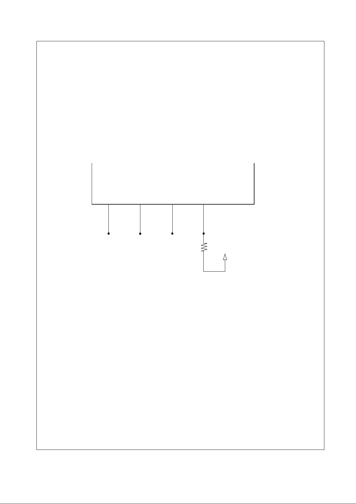
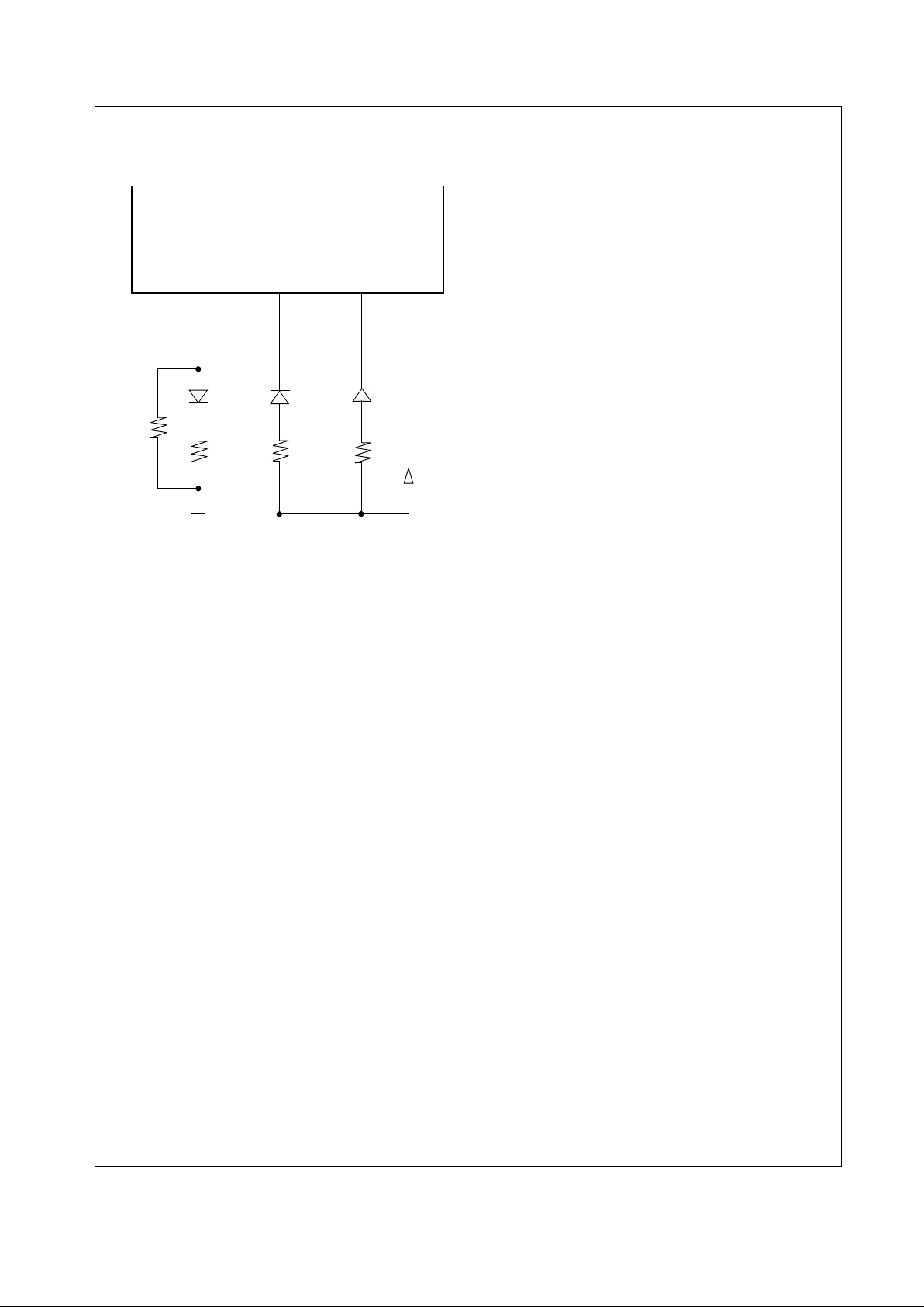
Figure 2. PHYAD Strapping Example
RXD0_A
RXD1_A
RXD0_B
RXD1_B
VCC
2.2kΩ
PHYAD1 = 1
PHYAD2 = 0PHY AD3 = 0
PHYAD4= 0

21 www.national.com
DP83849I
2.4 LED Interface
The DP83849I supports three configurable Light Emitting
Diode (LED) pins for each port.
Several functions can be multiplexed onto the three LEDs
using three different modes of operation. The LED operation mode can be selected by writing to the LED_CFG[1:0]
register bits in the PHY Control Register (PHYCR) at
address 19h, bits [6:5]. In addition, LED_CFG[0] for each
port can be set by a strap option on the CRS_A and
CRS_B pins. LED_CFG[1] is only controllable through reg
-
ister access and cannot be set by as strap pin.
See Table 3 for LED Mode selection.
The LED_LINK pin in Mode 1 indicates the link status of
the port. In 100BASE-T mode, link is established as a
result of input receive amplitude compliant with the TPPMD specifications which will result in internal generation
of signal detect. A 10 Mb/s Link is est abli shed as a result of
the reception of at least seven consecutive normal Link
Pulses or the reception of a valid 10BASE-T packet. This
will cause the as se rtion of LED_LINK. LED_LINK will dea s
sert in accordance with the Link Loss Timer as specified in
the IEEE 802.3 specification.
The LED_LINK p in in Mo de 1 w ill be OF F w h en no LI NK is
present.
The LED_LINK pin in Mode 2 and Mode 3 will be ON to
indicate Link is good and BLINK to indicate activity is
present on activity. The BLINK frequency is defined in
BLINK_FREQ, bits [7:6] of register LEDCR (18h).
Activity is defined as configured in LEDACT_RX, bit 8 of
register LEDCR (18h). If LEDACT_RX is 0, Activity is sig
naled for either transmit or receive. If LEDACT_RX is 1,
Activity is only signaled for receive.
The LED_SPEED pin indicates 10 or 100 Mb/s data rate of
the port. The LED is ON when operating in 100Mb/s mode
and OFF when operating in 10Mb/s mode. The functional
ity of this LED is independent of mode selected.
The LED_ACT/LED_COL pin in Mo de 1 ind ic ates the pre sence of either transmit or receive activity. The LED will be
ON for Activity and OFF for No Activity. In Mode 2, this pin
indicates the Collision status of the port. The LED will be
ON for Collision and OFF for No Collision.
The LED_ACT/LED_COL pin in Mode 3 indicates Duplex
status for 10 Mb/s or 100 Mb/s operation. The LED will be
ON for Full Duplex and OFF for Half Duplex.
In 10 Mb/s half duplex mode, the collision LED is based on
the COL signal.
Since these LED pins are also used as strap options, the
polarity of the LED is dependent on whether the pin is
pulled up or down.
2.4.1 LEDs
Since the Auto-Negotiation (AN) strap options share the
LED output pins, the external components required for
strapping and LED usage must be considered in order to
avoid contention.
Specifically, when the LED outputs are used to drive LEDs
directly, the active state of each output driver is dependent
on the logic level sampled by the corresponding AN input
upon power-up/reset. For example, if a given AN input is
resistively pulled low then the corresponding output will be
configured as an active high driver. Conversely, if a given
AN input is resistively pulled high, then the corresponding
output will be configured as an active low driver.
Refer to Figure 3 for an example of AN connections to
external components at port A. In this example, the AN
strapping results in Auto-Negotiation disabled with 100
Full-Duplex forced.
The adaptive nature of the LED outputs helps to simplify
potential implemen t ation issues o f th ese dual purpos e pins .
Table 3. LED Mode Select
Mode LED_CFG[1] LED_CFG[0] LED_LINK LED_SPEED LED_ACT/LED_COL
1 don’t care 1 ON for Good Link
OFF for No Link
ON in 100 Mb/s
OFF in 10 Mb/s
ON for Activity
OFF for No Activity
2 0 0 ON for Good Link
BLINK for Activity
ON in 100 Mb/s
OFF in 10 Mb/s
ON for Collision
OFF for No Collision
3 1 0 ON for Good Link
BLINK for Activity
ON in 100 Mb/s
OFF in 10 Mb/s
ON for Full Duplex
OFF for Half Duplex
22 www.national.com
DP83849I
2.4.2 LED Direct Control
The DP83849I provides another option to directly control
any or all LED outputs throu gh the LED Di rect Contro l Reg
ister (LEDCR), address 18h. The register does not provide
read access to LEDs.
2.5 Half Duplex vs. Full Duplex
The DP83849I supports both half and full duplex operation
at both 10 Mb/s and 100 Mb/s speeds.
Half-duplex relies on the C SMA/C D protoc ol to ha ndle c ollisions and network access. In Half-Duplex mode, CRS
responds to both transmit and receive activity in order to
maintain compliance with the IEEE 802.3 specification.
Since the DP83849I is designed to support simultaneous
transmit and receiv e act ivi ty it is capabl e of su ppor ting full duplex switched ap plications with a throughput of up to 20 0
Mb/s per port when operating in 100BASE-TX. Because
the CSMA/CD protocol does not apply to full-duplex opera
tion, the DP83849I disables its own internal collision sensing and reporting functions and modifies the behavior of
Carrier Sense (CRS) such that it indicates only receive
activity. This allows a full-duplex capable MAC to operate
properly.
All modes of operation (100BASE-TX, 10BASE-T) can run
either half-duplex or full-duplex. Additionally, other than
CRS and Collision reporting, all remaining MII signaling
remains the same regardless of the selected duplex mode.
It is important to understand that while Auto-Negotiation
with the use of Fast Link Pulse code words can interpret
and configure to full-duplex operation, parallel detection
can not recognize the difference between full and halfduplex from a fixed 10 Mb/s or 100 Mb/s link partner over
twisted pair. As specified in the 802.3u specification, if a
far-end link partner is configured to a forced full duplex
100BASE-TX ability, the parallel detection state machine in
the partner would be unable to detect the full duplex capa
bility of the far-end link partner. This link segment would
negotiate to a half duplex 100BASE-TX configuration
(same scenario for 10Mb/s).
2.6 Internal Loopback
The DP83849I includes a Loopback Test mode for facilitating system diagnostics. The Loopback mode is selected
through bit 14 (Loopback) of the Basic Mode Control Reg
ister (BMCR). Writing 1 to this bit enables MII transmit data
to be routed to the MII receive outputs. Loopback status
may be checked in bit 3 of the PHY Status Register
(PHYSTS). While in Loopback mode the data will not be
transmitted onto the media. To ensure that the desired
operating mode is maintained, Auto-Negotiation should be
disabled before selecting the Loopback mode.
2.7 BIST
The DP83849I incorporates an internal Built-in Self Test
(BIST) circuit to accommodate in-circuit testing or diagnos
tics. The BIST circuit can be utilized to test the integrity of
the transmit and receive data paths. BIST testing can be
performed with the part in the internal loopback mode or
externally looped back using a loopback cable fixture.
The BIST is implemented with independent transmit and
receive paths, with the tran smit block generating a continuous stream of a pseudo random sequence. The user can
select a 9 bit or 15 bit pseudo random sequence from the
PSR_15 bit in the PHY Control Register (PHYCR). The
received data is compared to the generated pseudo-ran
dom data by the BIST Linear Feedback Shift Register
(LFSR) to determine the BIST pass/fail status.
The pass/fail status of the BIST is stored in the BIST status
bit in the PHYCR regis ter. The status bit defaults to 0 (BIST
fail) and will transition on a successful comparison. If an
error (mis-compare) oc curs, the status bit is latched and is
cleared upon a subsequent write to the Start/Stop bit.
For transmit VOD testing, the Packet BIST Continuous
Mode can be used to allow continuous data transmission,
setting BIST_CONT_MODE, bit 5, of CDCTRL1 (1Bh).
The number of BIST errors can be monitored through the
BIST Error Count in the CDCTRL1 (1Bh), bits [15:8].
LED_LINK_A
LED_SPEED_A
LED_ACT/LED_COL_A
VCC
165Ω
165Ω
2.2kΩ
165Ω
AN0_A = 1
AN1_A = 1
AN_EN_A
= 0
GND
Figure 3. AN Strapping and LED Loading Example

23 www.national.com
DP83849I
3.0 MAC Interface
The DP83849I supports several modes of operation using
the MII interface pins. The optio ns are defi ned in th e follow
-
ing sections and include:
— MII Mode
— RMII Mode
— 10 Mb Serial Network Interface (SNI)
— Single Clock MII Mode (SCMII)
In addition, the DP83849 I suppo rt s the st and ard 802. 3u MII
Serial Management Interface and a Flexible MII Port
Assignment scheme.
The modes of operation can be selected by strap options
or register control. For RMII mode, it is recommended to
use the strap option, since it requires a 50 MHz clock
instead of the normal 25 MHz.
In each of these modes, the IEEE 802.3 serial management interface is operational for device configuration and
status. The serial management interface of the MII allows
for the configuration and control of multiple PHY devices,
gathering of status, error information, and the determina
-
tion of the type and ca pabilities of the attached PHY(s).
3.1 MII Interface
The DP83849I incorporates the Media Independent Interface (MII) as specified in Clause 22 of the IEEE 802.3u
standard. This interface may be used to connect PHY
devices to a MAC in 10/100 Mb/s systems. This section
describes the nibble wide MII data interface.
The nibble wide MII data interface consists of a rec ei ve bu s
and a transmit bus each with control signals to facilitate
data transfer between the PHY and the upper layer (MAC).
3.1.1 Nibble-wide MII Data Interface
Clause 22 of the IEEE 802.3u specification defines the
Media Independent Interface. This interface includes a
dedicated recei ve bu s an d a d edicated transmit bus. These
two data buses, along with various control and status sig
nals, allow for the simultaneous exchange of data between
the DP83849I and the upper layer agent (MAC).
The receive interface consists of a nibble wide data bus
RXD[3:0], a receive error signal RX_ER, a receive data
valid flag RX_DV, and a receive clock RX_CLK for syn
chronous transfer of the data. The receive clock operates
at either 2.5 MHz to su pport 10 Mb/s operation modes or at
25 MHz to support 100 Mb/s operational modes.
The transmit interface consists of a nibble wide data bus
TXD[3:0], a transmit enable control signal TX_EN, and a
transmit cloc k TX_CL K which runs at ei ther 2.5 MHz or 25
MHz.
Additionally, the MII includes the carrier sense signal CRS,
as well as a collision detect signal COL. The CRS signal
asserts to indicate the reception of data from the network
or as a function of transmit data in Half Duplex mode. The
COL signal asse rt s as an indication of a collision which ca n
occur during half-duplex operation when both a transmit
and receive operation occur simultaneously.
3.1.2 Collision Detect
For Half Duplex, a 10BASE-T or 100BASE-TX collision is
detected when the receive and transmit channels are
active sim ultaneously. Collisions are r eported by the COL
signal on the MII.
If the DP83849I is transmitting in 10 Mb/s mode when a
collision is dete cte d, the collision is not reported until seven
bits have been received while in the collision state. This
prevents a collision being reported incorrectly due to noise
on the network. The COL signal remains set for the dura
-
tion of the collision.
If a collision occ urs du ring a r eceive operation, it is immedi-
ately reported by the COL signal.
When heartbeat is enabled (only applicable to 10 Mb/s
operation), approximately 1
µs after the transmission of
each packet, a Si gn al Q u ali ty Error (SQE) signal of approximately 10 bit times is generated (internally) to indicate
successful transmiss io n. SQ E is repo rted as a pul se on th e
COL signal of the MII.
3.1.3 Carrier Sense
Carrier Sense (CRS) is asserted due to receive activity,
once valid data is detected via the squelch function during
10 Mb/s operation. During 100 Mb/s operation CRS is
asserted when a valid link (SD) and two non-contiguous
zeros are detected on the line.
For 10 or 100 Mb/s Half Duple x op era tio n, C RS is a sserte d
during either packet transmission or reception.
For 10 or 100 Mb/s Full Duplex operation, CRS is asserted
only due to receive activity.
CRS is deasserted following an end of packet.

24 www.national.com
DP83849I
3.2 Reduced MII Interface
The DP83849I incorporates the Reduced Media Independent Interface (RMII) as specified in the RMII specification
(rev1.2) from the RMII Consortium. This interface may be
used to connect PHY devices to a MAC in 10/100 Mb/s
systems using a reduced number of pins. In this mode,
data is transferred 2-bits at a time using the 50 MHz
RMII_REF clock for both transmit and receive. The follow
-
ing pins are used in RMII mode:
—TX_EN
—TXD[1:0]
— RX_ER (optional for Mac)
— CRS_DV
— RXD[1:0]
— X1 (RMII R eference clock is 50 MHz)
In addition, the RMII mode supplies an RX_DV signal
which allows for a simpler method of recovering receive
data without having to separate RX_DV from the CRS_DV
indication. This is especially useful for diagnostic testing
where it may be desirable to externally loop Receive MII
data directly to the transmitter.
The RX_ER output may be used by the MAC to detect
error conditions. It is asserted for symbol errors received
during a pack et, False Carrier even ts, and also for FIFO
underrun or overrun conditions. Since the Phy is required
to corrupt receive data on an error, a MAC is not required
to use RX_ER.
It is important to note that since both digital channels in the
DP83849I share the X1/RMII_REF input, both channels
must have RMII mod e ena bled or both channels must have
RMII mode disabled. Either channel may be in 10Mb or
100Mb mode in RMII or non-RMII mode.
Since the reference clock operates at 10 times the data
rate for 10 Mb/s operation, transmit data is sampled every
10 clocks. Likewise, receive data will be generated every
10th clock so that an attached device can sample the data
every 10 clocks.
RMII mode requires a 50 MHz oscillator be connected to
the device X1 pin. A 50 MHz crystal is not supported.
To tolerate potential frequency differences between the 50
MHz reference clock and the recovered receive clock, the
receive RMII function includes a programmable elasticity
buffer. The elasticity buffer is programmable to minimize
propagation delay based on expected packet size and
clock accuracy. This allows for supporting a range of
packet sizes including jumbo frames.
The elasticity buffer will force Frame Check Sequence
errors for packets which overrun or underrun the FIFO.
Underrun and Overrun conditions can be reported in the
RMII and Bypass Register (RBR). The following table indi
cates how to program the elastic ity buff er fifo (in 4-bi t increments) based on expected max packet size and clock
accuracy. It assumes both clocks (RMII Reference clock
and far-end Transmitter clock) have the same accuracy.
Packet lengths can be scaled linearly based on accuracy
(+/- 25ppm would allows packets twice as large). If the
threshold setting must support both 10Mb and 100Mb
operation, the setting should be made to support both
speeds.
Table 4. Supported packet sizes at +/-50ppm frequency accuracy
Start Threshold
RBR[1:0]
Latency Tolerance Recommended Packet Size
at +/- 50ppm
100Mb 10Mb 100Mb 10Mb
01 (default) 2 bits 8 bits 2,400 bytes 9,600 bytes
10 6 bits 4 bits 7,200 bytes 4,800 bytes
11 10 bits 8 bits 12,000 bytes 9,600 bytes
00 14 bits 12 bits 16,800 bytes 14,400 bytes

25 www.national.com
DP83849I
3.3 10 Mb Serial Network Interface (SNI)
The DP83849I incorporates a 10 Mb Serial Network Interface (SNI) which al lo ws a s im pl e ser ial d ata interface for 10
Mb only devices. This is also referred to as a 7-wire inter
face. While there is no defined standard for this interface, it
is based on early 10 Mb physical layer devices. Data is
clocked serially at 10 MHz using separate transmit and
receive paths. The following pins are used in SNI mode:
—TX_CLK
—TX_EN
—TXD[0]
—RX_CLK
—RXD[0]
— CRS
—COL
3.4 Single Clock MII Mode
Single Clock MII (SCMII) Mode allows MII operation using
a single 25MHz reference clock. Normal MII Mode requires
three clocks, a reference clock for physical layer functions,
a Transmit MII clock, and a Receive MII clock. Similar to
RMII mode, Single Clock MII mode requires only the refer
ence clock. In addition to reducing the number of pins
required, this mode allows the attached MAC device to use
only the reference clock domain. Since the DP83849I has
two ports, this ac tually reduce s the nu mber o f clock s from 6
to 1. A/C Timing requirements for SCMII operation are
similar to the RMII timing requirements.
For 10Mb operation, as in RMII mode, data is sampled and
driven every 10 clocks sinc e the refere nce clock is a t 10x
the data rate.
Separate control bits allow enabling the Transmit and
Receive Single Clock modes separately, allowing just
transmit or receive to operate in this mode. Control of Sin
gle Clock MII mode is through the RBR register.
Single Clock MII mode incorporates the use of the RMII
elasticity buffer, whic h is required to tolerate potential fre
quency differences between the 25MHz reference clock
and the recovered receive clock. Settings for the Elasticity
Buffer for SCMII mode are detailed in the following table.
Table 5. Supported SCMII pa cket sizes at +/-50ppm frequency accuracy
Start Threshold
RBR[1:0]
Latency Tolerance Recommended Packet Size
at +/- 50ppm
100Mb 10Mb 100Mb 10Mb
01 (default) 4 bits 8 bits 4,000 bytes 9,600 bytes
10 4 bits 8 bits 4,000 bytes 9,600 bytes
11 12 bits 8 bits 9.600 bytes 9,600 bytes
00 12 bits 8 bits 9,600 bytes 9,600 bytes
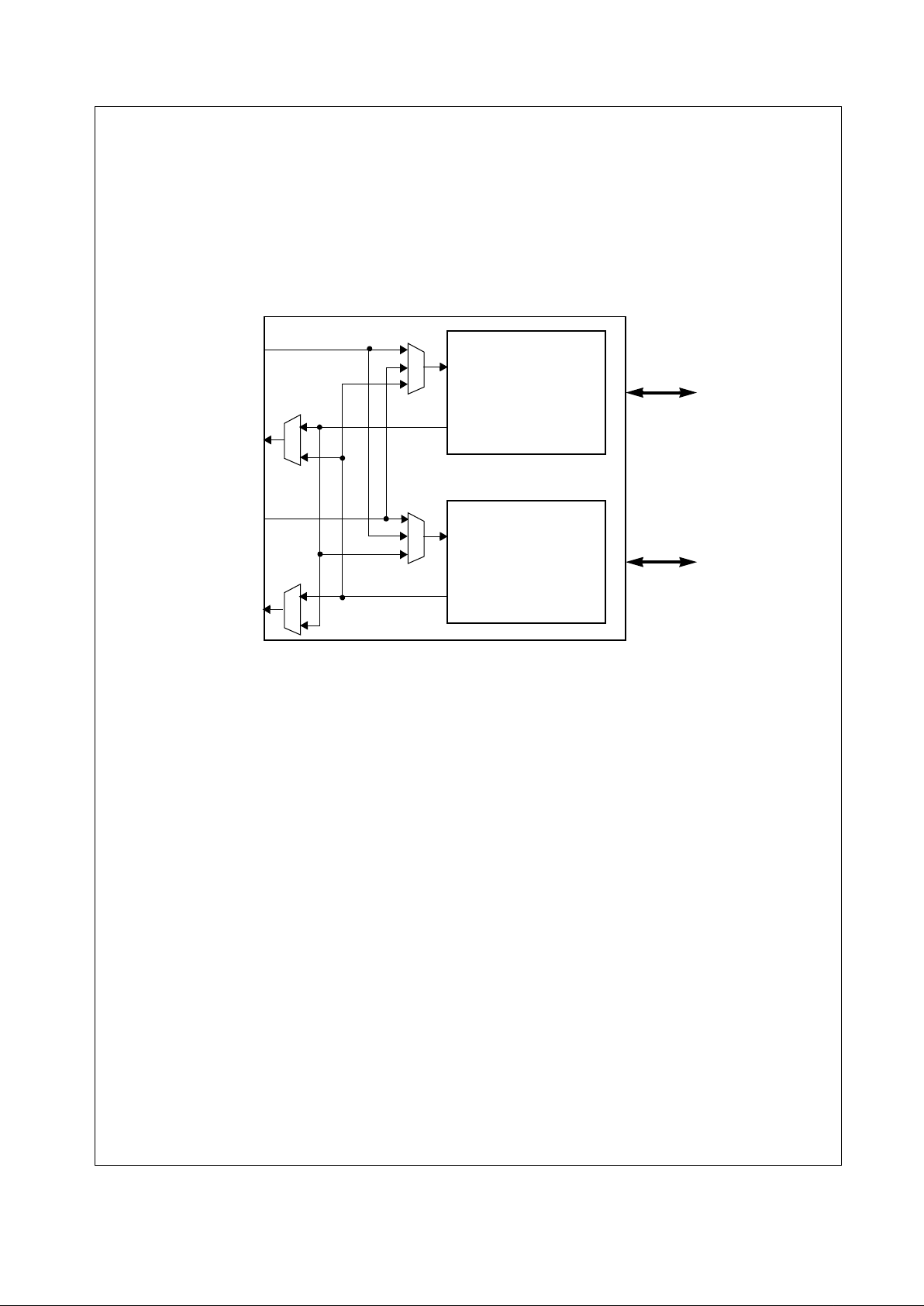
26 www.national.com
DP83849I
3.5 Flexible MII Port Assignment
The DP83849I supports a flexible assignment scheme for
each of the channels to the MII/RMII interface. Either of
the MII ports may be assigned to the internal channels A/B.
These values are contro lled by the R MII and Bypas s Reg
ister (RBR), address 17h. Transmit assignments and
Receive assignments can be made separately to allow
even more flexibility (i.e. both channels could transmit from
MII A while still allowing separate receive paths for the
channels).
In addition, the opposite receive channel may be used as
the transmit source for each channel. As shown in
Figure 4, Channel A receive data may be used as the
Channel B transmit data source while Channel B receive
data may be used as the Channel A transmit data source.
For proper clock synchronization, this function requires the
device be in RMII m ode o r Si ngl e Cl oc k MI I m od e o f ope ra
tion. A configuration strap is provided on pin 56,
RXD2_B/EXTENDER_EN to enable this mode.
MII
Channel A
Port
A
TX
RX
TX
RX
MII
Channel B
Port
B
TX
RX
TX
RX
10BASE-T
or
100BASE-TX
10BASE-T
or
100BASE-TX
Figure 4. MII Port Mapping

27 www.national.com
DP83849I
3.5.1 RX MII Port Mapping
Note that Channel A is the master of MII Port A, and Channel B is the master of MII Port B. This means that in order
for Channel B to control MII Port A, Channel A must be
configured t o either cont rol MII Po rt B or be Disa bled; the
reverse is also true.
RX MII Port Mapping controls and configurations are
shown in the following tables:
Table 6. RX MII Port Mapping Controls
Table 7. RX MII Port Mapping Configurations
RBR[12:11] Desired RX Channel Destination
00 Normal Port
01 Opposite Port
10 Both Ports
11 Disabled
Channel A RBR[12:11] Channel B RBR[12:11] RX MII Port A Source RX MII Port B Source
00 00 Channel A Channel B
00 01 Channel A Channel B
00 10 Channel A Channel B
00 11 Channel A Disabled
01 00 Channel A Channel B
01 01 Channel B Channel A
01 10 Channel B Channel A
01 11 Disabled Channel A
10 00 Channel A Channel B
10 01 Channel B Channel A
10 10 Channel A Channel B
10 11 Channel A Channel A
11 00 Disabled Channel B
11 01 Channel B Disabled
11 10 Channel B Channel B
11 11 Disabled Disabled

28 www.national.com
DP83849I
3.5.2 TX MII Port Mapping
TX MII Port Mapping controls and configurations are
shown in the following tables:
Table 8. TX MII Port Mapping Controls
Table 9. TX MII Port Mapping Configurations
3.5.3 Common Flexible MII Port Configurations
Table 10. Common Flexible MII Port Configurations
RBR[10:9] TX Channel Source
00 Normal Port
01 Opposite Port
10 Opposite RX Port
11 Disabled
Channel A RBR[10:9] Port A TX Source Channel B RBR[10:9] Port B TX Source
00 MII Port A 00 MII Port B
01 MII Port B 01 MII Port A
10 RX Channel B 10 RX Channel A
11 Disabled 11 Disabled
Mode Channel A
RBR[12:9]
Channel B
RBR[12:9]
Description
Normal 0000 0000 MII port A assigned to Channel A, MII
Port B assigned to Channel B
Full Port Swap 0101 0101 MII port A assigned to Channel B, MII
Port B assigned to Channel A
Extender 1110 1110 MII RX disabled, Channel A transmits
from Channel B RX data, Channel B
transmits from Channel A RX data
Broadcast TX MII Port A xx00 xx01 Both Channels transmit from TX MII
Port A
Broadcast TX MII Port B xx01 xx00 Both Channels transmit from TX MII
Port B
Mirror RX Channel A 10xx 11xx Channel A RX traffic appears on both
Ports.
Mirror RX Channel B 11xx 10xx Channel B RX traffic appears on both
Ports.
Disable Port A 1111 xxxx MII Port A is disabled
Disable Port B xxxx 1111 MII Port B is disabled

29 www.national.com
DP83849I
3.5.4 Strapped Extender Mode
The DP83849I provides a simple strap option to automatically configure both channels for Extender Mode with no
device register configuration necessary. The
EXTENDER_EN Strap can be used in conjunction with the
Auto-Negotiation Straps (AN_EN, AN0, AN1), the RMII
Mode Strap to allow many possible configurations. If
Extender Mode is strapped but RMII Mode is not, both
channels will automatically be configured for Single Clock
MII Receive and Transmit Modes. The optional use of
RMII Mode in co njun cti on wi th E xte nde r Mode a llo ws f lexi
-
bility in the system design.
Several common configurations are shown in Table 11.
Table 11. Common Strapped Extender Mode Configurations
3.5.5 Notes and Restrictions
— Extender: Both channels mus t be operating at th e same
speed (10 or 100Mb). This can be acco mplis hed us ing
straps or channel re gister contro ls. Bo th ch annels must
be in Full Duplex mode. Bo th channels must eithe r be in
RMII Mode (RBR:RMII_EN = 1) or full Single Clock MII
Mode (RBR:SCMII_RX = 1 and RBR:SCMII_TX = 1) to
ensure synchronous operation.
If only one RX to TX path
is enabled, SCMII_RX in the RX channel (RBR regist er
17h bit 7) and SCMII_TX in the TX channel (RBR regis
-
ter 17h bit 6) must be set to 1.
— Broadcast TX MII Port Mode: To ensure sync hro nou s
operation, both channels must be in RMII Mode (RBR
register 17h bit 5 = 1) or in Single Clock TX MII Mode
(RBR register 17h bit 6 = 1). Both channels must be op
erating at the same speed (10 or 100Mb). Both channels
must be in Full Duplex mode to ensure no collisions are
seen. This is because in Single Clock TX MII Mode, a
collision on one PHY channel would cause both chan
-
nels to send the Jam pattern.
— RMII Mode: Both Channels must have RMII Mode en-
abled or disabled concurrently due to the internal reference clocking scheme. In Full Port Swap Mode,
Channels are not required to have a common speed.
— 10Base- T Serial Mode: This MAC- side mode, also
known as Serial Network Interface (SNI), may not be
used when both channels share data connections (Ex
tender or Broadcast TX MII Port). This is due to the requirement of synchro nous op era tion be tween ch ann els,
which is not supported in SNI Mode.
— CRS Assignment: When a channel is n ot in RMII M ode,
its associated CRS pin is sourced from the transmitter
and controlled by the TX MII Port Ass ignment, bits [10:9]
of RBR (17h). When a channel is in RMII Mode, the as
-
sociated CRS pin is sourced from the receiver and controlled by the RX MII Port Assignment, bits [12:11] of
RBR (17h).
— Output Enables: Flexible MII Port Assignment does not
control signal output enables.
— Test Modes: Test modes are not designed to be com-
patible with Flexible MII Port Selection, which assumes
default MII pin directions.
— LED Assignment: LEDs are associated with their re-
spective digital channels, and therefore do not get
mapped to alternate channels. For example, assertion
of LED_LINK_A indicate s valid lin k status fo r Channel A
independent of the MII Port Assignment.
— Straps: Strap pins are always associated with their re-
spective channel, i.e. a strap on RX_ER_A is used by
Channel A.
— Port Isolate Mode: Each MII port’s Isolate function, bit
10 of BMCR (00h) is always associated with its respec
tive channel, i. e. the Isolat e func tion fo r Port A i s alwa ys
controlled by Channel A’s BMCR (00h). Due to the var
ious possible combi nation s of TX and RX po rt selectio n,
it may not be advisable to place a port in Isolate mode.
— Energy Detect and Powerdown Modes: The output
enables for each MII port are alwa ys controlled b y the re
spective channel Energy Detect and Powerdown functions. These functions shoul d be dis abled wh eneve r an
MII port is in use b ut not ass igned to its defau lt chann el.
Note that Extender/Media Converter modes allow the
use of Energy Detect and Powerdown modes if the RX
MII ports are not in use.
Mode Auto-Negotiation Straps
100Mb Copper Extender Both channels are forced to 100Mb Full Duplex
10Mb Copper Extender Both channels are forced to 10Mb Full Duplex
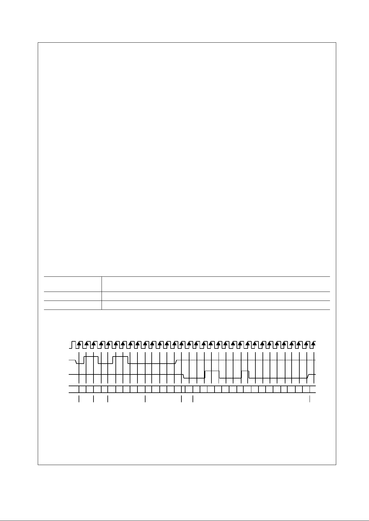
30 www.national.com
DP83849I
3.6 802.3u MII Serial Management Interface
3.6.1 Serial Management Register Access
The serial management MII specification defines a set of
thirty-two 16-bit status and control registers that are acces
sible through the management interface pins MDC and
MDIO. The DP83849I implements all the required MII reg
isters as well as several optional registers. These registers
are fully described in Section 7.0. A descri ption of the serial
management access protocol follows.
3.6.2 Serial Management Access Protocol
The serial cont rol interface co nsists of two pins, Management Data Clock (MDC) and Management Data Input/Output (MDIO). MDC has a maximum clock rate of 25 MHz
and no minimum rate. The MDIO line is bi-directional and
may be shared by up to 32 devices. The MDIO frame for
mat is shown below in Table 12.
In addition, the MDIO pin requires a pull-up resistor (1.5
k
Ω) which, during IDLE and turnaround, will pull MDIO
high. In order to initialize the MDIO interface, the station
management entity sends a sequence of 32 contiguous
logic ones on MDIO to provide the DP83849I with a
sequence that can be used to establish synchronization.
This preamble may be generated either by driving MDIO
high for 32 consecutive MDC clock cycles, or by simply
allowing the MDIO p ull-up r esi stor to pull th e MDIO pin hig h
during which time 32 MDC clock cycles are provided. In
addition 32 MDC clock cycles should be used to re-sync
the device if an invalid start, opcode, or turnaround bit is
detected.
The DP83849I waits until it has received this preamble
sequence before responding to any other transaction.
Once the DP83849I serial management port has been ini
tialized no further preamble sequencing is required until
after a power-on/reset, invalid Start, invalid Opcode, or
invalid turnaround bit has occurred.
The St art co de is in dic ate d by a <01> p atte rn. Th is ass ure s
the MDIO line transitions from the default idle line state.
Turnaround is defined as an idle bit time inserted between
the Register Address field and the Data field. To avoid contention during a read transaction, no device shall actively
drive the MDIO signal during the first bit of Turnaround.
The addressed DP83849I drives the MDIO with a zero for
the second bit of turnaround and follows this with the
required data.
Figure 5 shows the timing relationship
between MDC and th e MDIO as dr iven/re ceived by the Station (STA) and the DP83849I (PHY) for a typical register
read access.
For write transactions, the station management entity
writes data to the addresse d DP838 49I thus eli mina ting the
requirement for MDIO Turnaround. The Turnaround time is
filled by the management entity by inserting <10>.
Figure 6
shows the timing relationship for a typical MII register write
access.
Table 12. Typical MDIO Frame Format
Figure 5. Typical MDC/MDIO Read Operation
MII Management
Serial Protocol
<idle><start><op code><device addr><reg addr><turnaround><data><idle>
Read Operation <idle><01><10><AAAAA><RRRRR><Z0><xxxx xxxx xxxx xxxx><i d le>
Write Operation <idle><01><01><AAAAA><RRRRR><10><xxxx xxxx xxxx xxxx><idle>
MDC
MDIO
00011 110000000
(STA)
Idle Start
Opcode
(Read)
PHY Address
(PHYAD = 0Ch)
Register Address
(00h = BMCR)
TA
Register Data
Z
MDIO
(PHY)
Z
Z
Z
0 0 011000100000000
Z
Idle
Z
Z
 Loading...