

NSC DP83848IVV, DP83848I Datasheet
© 2007 National Semiconductor Corporation www.national.com
1
DP83848I PHYTER
®
— Industrial Temperature Single Port 10/100 Mb/s Ethernet Physical Layer Transceiver
February 2007
DP83848I PHYTER® - Industrial Temperature
Single Port 10/100 Mb/s Ethernet Physical Layer Transceiver
General Description
The DP83848I is a robust fully featured 10/100 single
port Physical Layer device offering low power consumption, including several intelligent power down
states. These low power modes increase overall product reliability due to decre ased powe r dissi pat ion. Supporting multiple intelligent power modes allows the
application to use the absolute minimum amount of
power needed for operation. In addition to low power,
the DP83848I is optimized for cable length performance far exceeding IEEE specifications.
The DP83848I includes a 25MHz clock out. This
means that the application can be designed with a
minimum of external parts, which in turn results in the
lowest possible total cost of the solution.
The DP83848I easily interfaces to twisted pair media
via an external transformer and fully supports JTAG
IEEE specification 1149.1 for ease of manufacturing.
Additionally both MII and RMII are supported ensuring
ease and flexibility of design.
The DP83848I features integrated sublayers to support both 10BASE-T and 100BASE-TX Ethernet pro tocols, which ensures compatibility and interoperability
with all other standards based Ethernet solutions.
The DP83848I is offered in a small form factor (48 pin
LQFP) so that a minimum of board space is needed.
Applications
• High End Peripheral Devices
• Industrial Controls and Factory Automation
• General Embedded Applications
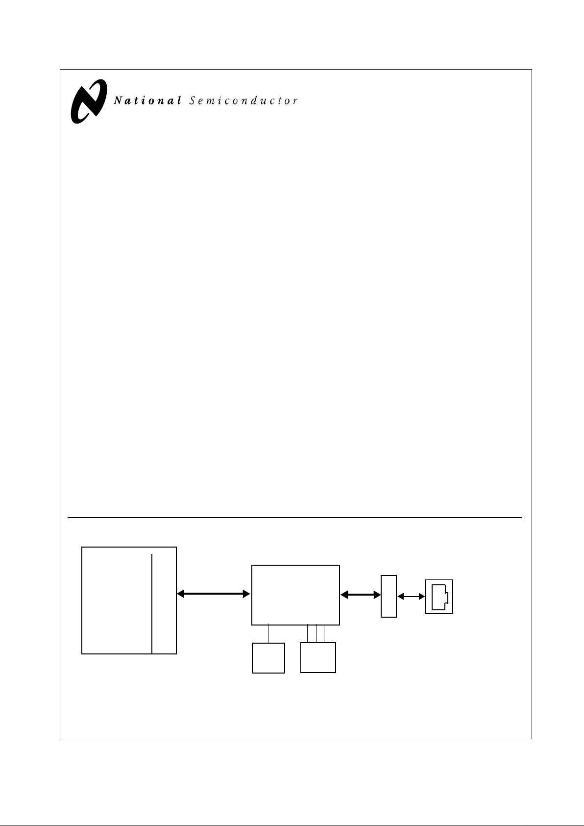
System Diagram
PHYTER® is a registered trademark of National Semiconductor.
Status
10BASE-T
or
100BASE-TX
MII/RMII/SNI
25 MHz
Magnetics
RJ-45
Clock
LEDs
DP83848I
10/100 Mb/s
Media Access Controller
MPU/CPU
Source
Typical Application
Features
• Low-power 3.3V, 0.18µm CMOS technology
• Low power consumption < 270mW Typical
• 3.3V MAC Interface
• Auto-MDIX for 10/100 Mb/s
• Energy Detection Mode
• 25 MHz clock out
• SNI Interface (configurable)
• RMII Rev. 1.2 Interface (configurable)
• MII Serial Management Interface (MDC and MDIO)
• IEEE 802.3u MII
• IEEE 802.3u Auto-Negotiation and Parallel Detection
• IEEE 802.3u ENDEC, 10BASE-T transceivers and filters
• IEEE 802.3u PCS, 100BASE-TX transceivers and filters
• IEEE 1149.1 JTAG
• Integrated ANSI X3.263 compliant TP-PMD physical sub-
layer with adaptive equalization and Baseline Wander compensation
• Error-free Operation up to 150 meters
• Programmable LED support Link, 10 /100 Mb/s Mode, Activ-
ity, and Collision Detect
• Single register access for complete PHY status
• 10/100 Mb/s packet BIST (Built in Self Test)
• 48-pin LQFP package (7mm) x (7mm)
2 www.national.com
DP83848I
SERIAL
MANAGEMENT
TX_CLK
TXD[3:0]
TX_EN
MDIO
MDC
COL
CRS/CRS_DV
RX_ER
RX_DV
RXD[3:0]
RX_CLK
Auto-Negotiation
State Machine
Clock
RX_DATA
RX_CLK
TX_DATA TX_CLK
REFERENCE CLOCK
TD±
RD±
LEDS
Generation
MII/RMII/SNI INTERFACES
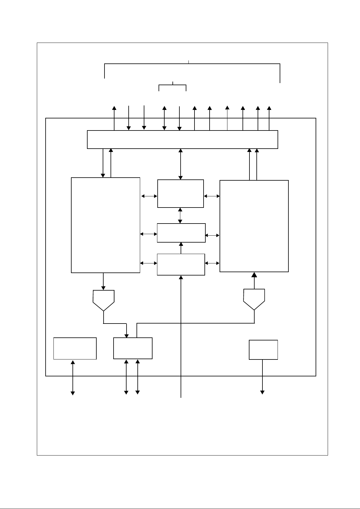
Figure 1. DP83848I Functional Block Diagram
MII
Registers
Transmit
Block
10BASE-T &
100BASE-TX
10BASE-T &
100BASE-TX
Receive
Block
Auto-MDIX
Boundary
Scan
DAC
ADC
JTAG
LED
Drivers
MII/RMII/SNI

3 www.national.com
DP83848I
Table of Contents
1.0 Pin Descriptions . . . . . . . . . . . . . . . . . . . . . . . . . . . . . . . . . . . . . . . . . . . . . . . . . 9
1.1 Serial Management Interface . . . . . . . . . . . . . . . . . . . . . . . . . . . . . . . . . . . . . . . . . . . . . . .9
1.2 MAC Data Interface . . . . . . . . . . . . . . . . . . . . . . . . . . . . . . . . . . . . . . . . . . . . . . . . . . . . . .9
1.3 Clock Interface . . . . . . . . . . . . . . . . . . . . . . . . . . . . . . . . . . . . . . . . . . . . . . . . . . . . . . . . .11
1.4 LED Interface . . . . . . . . . . . . . . . . . . . . . . . . . . . . . . . . . . . . . . . . . . . . . . . . . . . . . . . . . .11
1.5 JTAG Interface . . . . . . . . . . . . . . . . . . . . . . . . . . . . . . . . . . . . . . . . . . . . . . . . . . . . . . . . .12
1.6 Reset and Power Down . . . . . . . . . . . . . . . . . . . . . . . . . . . . . . . . . . . . . . . . . . . . . . . . . .12
1.7 Strap Options . . . . . . . . . . . . . . . . . . . . . . . . . . . . . . . . . . . . . . . . . . . . . . . . . . . . . . . . . .12
1.8 10 Mb/s and 100 Mb/s PMD Interface . . . . . . . . . . . . . . . . . . . . . . . . . . . . . . . . . . . . . . .14
1.9 Special Connections . . . . . . . . . . . . . . . . . . . . . . . . . . . . . . . . . . . . . . . . . . . . . . . . . . . . .14
1.10 Power Supply Pins . . . . . . . . . . . . . . . . . . . . . . . . . . . . . . . . . . . . . . . . . . . . . . . . . . . . .14
1.11 Package Pin Assignments . . . . . . . . . . . . . . . . . . . . . . . . . . . . . . . . . . . . . . . . . . . . . . .15
2.0 Configuration . . . . . . . . . . . . . . . . . . . . . . . . . . . . . . . . . . . . . . . . . . . . . . . . . . 16
2.1 Auto-Negotiation . . . . . . . . . . . . . . . . . . . . . . . . . . . . . . . . . . . . . . . . . . . . . . . . . . . . . . . .16
2.1.1 Auto-Negotiation Pin Control . . . . . . . . . . . . . . . . . . . . . . . . . . . . . . . . . . . . . . . . . . . . . . . . . 16
2.1.2 Auto-Negotiation Register Control . . . . . . . . . . . . . . . . . . . . . . . . . . . . . . . . . . . . . . . . . . . . . 16
2.1.3 Auto-Negotiation Parallel Detection . . . . . . . . . . . . . . . . . . . . . . . . . . . . . . . . . . . . . . . . . . . . 17
2.1.4 Auto-Negotiation Restart . . . . . . . . . . . . . . . . . . . . . . . . . . . . . . . . . . . . . . . . . . . . . . . . . . . . 17
2.1.5 Enabling Auto-Negotiation via Software . . . . . . . . . . . . . . . . . . . . . . . . . . . . . . . . . . . . . . . . 17
2.1.6 Auto-Negotiation Complete Time . . . . . . . . . . . . . . . . . . . . . . . . . . . . . . . . . . . . . . . . . . . . . . 17
2.2 Auto-MDIX . . . . . . . . . . . . . . . . . . . . . . . . . . . . . . . . . . . . . . . . . . . . . . . . . . . . . . . . . . . .17
2.3 PHY Address . . . . . . . . . . . . . . . . . . . . . . . . . . . . . . . . . . . . . . . . . . . . . . . . . . . . . . . . . .18
2.3.1 MII Isolate Mode . . . . . . . . . . . . . . . . . . . . . . . . . . . . . . . . . . . . . . . . . . . . . . . . . . . . . . . . . . 18
2.4 LED Interface . . . . . . . . . . . . . . . . . . . . . . . . . . . . . . . . . . . . . . . . . . . . . . . . . . . . . . . . . .19
2.4.1 LEDs . . . . . . . . . . . . . . . . . . . . . . . . . . . . . . . . . . . . . . . . . . . . . . . . . . . . . . . . . . . . . . . . . . . 19
2.4.2 LED Direct Control . . . . . . . . . . . . . . . . . . . . . . . . . . . . . . . . . . . . . . . . . . . . . . . . . . . . . . . . . 20
2.5 Half Duplex vs. Full Duplex . . . . . . . . . . . . . . . . . . . . . . . . . . . . . . . . . . . . . . . . . . . . . . .20
2.6 Internal Loopback . . . . . . . . . . . . . . . . . . . . . . . . . . . . . . . . . . . . . . . . . . . . . . . . . . . . . . .20
2.7 BIST . . . . . . . . . . . . . . . . . . . . . . . . . . . . . . . . . . . . . . . . . . . . . . . . . . . . . . . . . . . . . . . . .20
3.0 Functional Description. . . . . . . . . . . . . . . . . . . . . . . . . . . . . . . . . . . . . . . . . . . 21
3.1 MII Interface . . . . . . . . . . . . . . . . . . . . . . . . . . . . . . . . . . . . . . . . . . . . . . . . . . . . . . . . . . .21
3.1.1 Nibble-wide MII Data Interface . . . . . . . . . . . . . . . . . . . . . . . . . . . . . . . . . . . . . . . . . . . . . . . . 21
3.1.2 Collision Detect . . . . . . . . . . . . . . . . . . . . . . . . . . . . . . . . . . . . . . . . . . . . . . . . . . . . . . . . . . . 21
3.1.3 Carrier Sense . . . . . . . . . . . . . . . . . . . . . . . . . . . . . . . . . . . . . . . . . . . . . . . . . . . . . . . . . . . . . 21
3.2 Reduced MII Interface . . . . . . . . . . . . . . . . . . . . . . . . . . . . . . . . . . . . . . . . . . . . . . . . . . .21
3.3 10 Mb Serial Network Interface (SNI) . . . . . . . . . . . . . . . . . . . . . . . . . . . . . . . . . . . . . . . .22
3.4 802.3u MII Serial Management Interface . . . . . . . . . . . . . . . . . . . . . . . . . . . . . . . . . . . . .22
3.4.1 Serial Management Register Access . . . . . . . . . . . . . . . . . . . . . . . . . . . . . . . . . . . . . . . . . . . 22
3.4.2 Serial Management Access Protocol . . . . . . . . . . . . . . . . . . . . . . . . . . . . . . . . . . . . . . . . . . . 22
3.4.3 Serial Management Preamble Suppression . . . . . . . . . . . . . . . . . . . . . . . . . . . . . . . . . . . . . 23
4.0 Architecture. . . . . . . . . . . . . . . . . . . . . . . . . . . . . . . . . . . . . . . . . . . . . . . . . . . . 24
4.1 100BASE-TX TRANSMITTER . . . . . . . . . . . . . . . . . . . . . . . . . . . . . . . . . . . . . . . . . . . . .24
4.1.1 Code-group Encoding and Injection . . . . . . . . . . . . . . . . . . . . . . . . . . . . . . . . . . . . . . . . . . . . 26
4.1.2 Scrambler . . . . . . . . . . . . . . . . . . . . . . . . . . . . . . . . . . . . . . . . . . . . . . . . . . . . . . . . . . . . . . . . 26
4.1.3 NRZ to NRZI Encoder . . . . . . . . . . . . . . . . . . . . . . . . . . . . . . . . . . . . . . . . . . . . . . . . . . . . . . 26
4.1.4 Binary to MLT-3 Convertor . . . . . . . . . . . . . . . . . . . . . . . . . . . . . . . . . . . . . . . . . . . . . . . . . . . 26
4.2 100BASE-TX RECEIVER . . . . . . . . . . . . . . . . . . . . . . . . . . . . . . . . . . . . . . . . . . . . . . . . .26
4.2.1 Analog Front End . . . . . . . . . . . . . . . . . . . . . . . . . . . . . . . . . . . . . . . . . . . . . . . . . . . . . . . . . . 26
4.2.2 Digital Signal Processor . . . . . . . . . . . . . . . . . . . . . . . . . . . . . . . . . . . . . . . . . . . . . . . . . . . . . 26
4.2.2.1 Digital Adaptive Equalization and Gain Control . . . . . . . . . . . . . . . . . . . . . . . . . . . . . . 28
4.2.2.2 Base Line Wander Compensation . . . . . . . . . . . . . . . . . . . . . . . . . . . . . . . . . . . . . . . . 29
4.2.3 Signal Detect . . . . . . . . . . . . . . . . . . . . . . . . . . . . . . . . . . . . . . . . . . . . . . . . . . . . . . . . . . . . . 29
4.2.4 MLT-3 to NRZI Decoder . . . . . . . . . . . . . . . . . . . . . . . . . . . . . . . . . . . . . . . . . . . . . . . . . . . . . 29
4.2.5 NRZI to NRZ . . . . . . . . . . . . . . . . . . . . . . . . . . . . . . . . . . . . . . . . . . . . . . . . . . . . . . . . . . . . . 29
4.2.6 Serial to Parallel . . . . . . . . . . . . . . . . . . . . . . . . . . . . . . . . . . . . . . . . . . . . . . . . . . . . . . . . . . . 29
4.2.7 Descrambler . . . . . . . . . . . . . . . . . . . . . . . . . . . . . . . . . . . . . . . . . . . . . . . . . . . . . . . . . . . . . . 30

4 www.national.com
DP83848I
4.2.8 Code-group Alignment . . . . . . . . . . . . . . . . . . . . . . . . . . . . . . . . . . . . . . . . . . . . . . . . . . . . . . 30
4.2.9 4B/5B Decoder . . . . . . . . . . . . . . . . . . . . . . . . . . . . . . . . . . . . . . . . . . . . . . . . . . . . . . . . . . . . 30
4.2.10 100BASE-TX Link Integrity Monitor . . . . . . . . . . . . . . . . . . . . . . . . . . . . . . . . . . . . . . . . . . . 30
4.2.11 Bad SSD Detection . . . . . . . . . . . . . . . . . . . . . . . . . . . . . . . . . . . . . . . . . . . . . . . . . . . . . . . 30
4.3 10BASE-T TRANSCEIVER MODULE . . . . . . . . . . . . . . . . . . . . . . . . . . . . . . . . . . . . . . .30
4.3.1 Operational Modes . . . . . . . . . . . . . . . . . . . . . . . . . . . . . . . . . . . . . . . . . . . . . . . . . . . . . . . . . 30
4.3.2 Smart Squelch . . . . . . . . . . . . . . . . . . . . . . . . . . . . . . . . . . . . . . . . . . . . . . . . . . . . . . . . . . . . 31
4.3.3 Collision Detection and SQE . . . . . . . . . . . . . . . . . . . . . . . . . . . . . . . . . . . . . . . . . . . . . . . . . 31
4.3.4 Carrier Sense . . . . . . . . . . . . . . . . . . . . . . . . . . . . . . . . . . . . . . . . . . . . . . . . . . . . . . . . . . . . . 31
4.3.5 Normal Link Pulse Detection/Generation . . . . . . . . . . . . . . . . . . . . . . . . . . . . . . . . . . . . . . . . 31
4.3.6 Jabber Function . . . . . . . . . . . . . . . . . . . . . . . . . . . . . . . . . . . . . . . . . . . . . . . . . . . . . . . . . . . 32
4.3.7 Automatic Link Polarity Detection and Correction . . . . . . . . . . . . . . . . . . . . . . . . . . . . . . . . . 32
4.3.8 Transmit and Receive Filtering . . . . . . . . . . . . . . . . . . . . . . . . . . . . . . . . . . . . . . . . . . . . . . . 32
4.3.9 Transmitter . . . . . . . . . . . . . . . . . . . . . . . . . . . . . . . . . . . . . . . . . . . . . . . . . . . . . . . . . . . . . . . 32
4.3.10 Receiver . . . . . . . . . . . . . . . . . . . . . . . . . . . . . . . . . . . . . . . . . . . . . . . . . . . . . . . . . . . . . . . . 32
5.0 Design Guidelines. . . . . . . . . . . . . . . . . . . . . . . . . . . . . . . . . . . . . . . . . . . . . . . 33
5.1 TPI Network Circuit . . . . . . . . . . . . . . . . . . . . . . . . . . . . . . . . . . . . . . . . . . . . . . . . . . . . . .33
5.2 ESD Protection . . . . . . . . . . . . . . . . . . . . . . . . . . . . . . . . . . . . . . . . . . . . . . . . . . . . . . . . .34
5.3 Clock In (X1) Requirements . . . . . . . . . . . . . . . . . . . . . . . . . . . . . . . . . . . . . . . . . . . . . . .34
5.4 Power Feedback Circuit . . . . . . . . . . . . . . . . . . . . . . . . . . . . . . . . . . . . . . . . . . . . . . . . . .35
5.5 Power Down/Interrupt . . . . . . . . . . . . . . . . . . . . . . . . . . . . . . . . . . . . . . . . . . . . . . . . . . . .35
5.5.1 Power Down Control Mode . . . . . . . . . . . . . . . . . . . . . . . . . . . . . . . . . . . . . . . . . . . . . . . . . . 35
5.5.2 Interrupt Mechanisms . . . . . . . . . . . . . . . . . . . . . . . . . . . . . . . . . . . . . . . . . . . . . . . . . . . . . . 35
5.6 Energy Detect Mode . . . . . . . . . . . . . . . . . . . . . . . . . . . . . . . . . . . . . . . . . . . . . . . . . . . . .35
6.0 Reset Operation . . . . . . . . . . . . . . . . . . . . . . . . . . . . . . . . . . . . . . . . . . . . . . . . 36
6.1 Hardware Reset . . . . . . . . . . . . . . . . . . . . . . . . . . . . . . . . . . . . . . . . . . . . . . . . . . . . . . . .36
6.2 Software Reset . . . . . . . . . . . . . . . . . . . . . . . . . . . . . . . . . . . . . . . . . . . . . . . . . . . . . . . . .36
7.0 Register Block . . . . . . . . . . . . . . . . . . . . . . . . . . . . . . . . . . . . . . . . . . . . . . . . . 37
7.1 Register Definition . . . . . . . . . . . . . . . . . . . . . . . . . . . . . . . . . . . . . . . . . . . . . . . . . . . . . .40
7.1.1 Basic Mode Control Register (BMCR) . . . . . . . . . . . . . . . . . . . . . . . . . . . . . . . . . . . . . . . . . . 41
7.1.2 Basic Mode Status Register (BMSR) . . . . . . . . . . . . . . . . . . . . . . . . . . . . . . . . . . . . . . . . . . . 43
7.1.3 PHY Identifier Register #1 (PHYIDR1) . . . . . . . . . . . . . . . . . . . . . . . . . . . . . . . . . . . . . . . . . . 44
7.1.4 PHY Identifier Register #2 (PHYIDR2) . . . . . . . . . . . . . . . . . . . . . . . . . . . . . . . . . . . . . . . . . . 44
7.1.5 Auto-Negotiation Advertisement Register (ANAR) . . . . . . . . . . . . . . . . . . . . . . . . . . . . . . . . . 44
7.1.6 Auto-Negotiation Link Partner Ability Register (ANLPAR) (BASE Page) . . . . . . . . . . . . . . . . 46
7.1.7 Auto-Negotiation Link Partner Ability Register (ANLPAR) (Next Page) . . . . . . . . . . . . . . . . . 47
7.1.8 Auto-Negotiate Expansion Register (ANER) . . . . . . . . . . . . . . . . . . . . . . . . . . . . . . . . . . . . . 47
7.1.9 Auto-Negotiation Next Page Transmit Register (ANNPTR) . . . . . . . . . . . . . . . . . . . . . . . . . . 48
7.2 Extended Registers . . . . . . . . . . . . . . . . . . . . . . . . . . . . . . . . . . . . . . . . . . . . . . . . . . . . .49
7.2.1 PHY Status Register (PHYSTS) . . . . . . . . . . . . . . . . . . . . . . . . . . . . . . . . . . . . . . . . . . . . . . 49
7.2.2 MII Interrupt Control Register (MICR) . . . . . . . . . . . . . . . . . . . . . . . . . . . . . . . . . . . . . . . . . . 51
7.2.3 MII Interrupt Status and Misc. Control Register (MISR) . . . . . . . . . . . . . . . . . . . . . . . . . . . . . 52
7.2.4 False Carrier Sense Counter Register (FCSCR) . . . . . . . . . . . . . . . . . . . . . . . . . . . . . . . . . . 53
7.2.5 Receiver Error Counter Register (RECR) . . . . . . . . . . . . . . . . . . . . . . . . . . . . . . . . . . . . . . . 53
7.2.6 100 Mb/s PCS Configuration and Status Register (PCSR) . . . . . . . . . . . . . . . . . . . . . . . . . . 54
7.2.7 RMII and Bypass Register (RBR) . . . . . . . . . . . . . . . . . . . . . . . . . . . . . . . . . . . . . . . . . . . . . 55
7.2.8 LED Direct Control Register (LEDCR) . . . . . . . . . . . . . . . . . . . . . . . . . . . . . . . . . . . . . . . . . . 55
7.2.9 PHY Control Register (PHYCR) . . . . . . . . . . . . . . . . . . . . . . . . . . . . . . . . . . . . . . . . . . . . . . . 56
7.2.10 10Base-T Status/Control Register (10BTSCR) . . . . . . . . . . . . . . . . . . . . . . . . . . . . . . . . . . 57
7.2.11 CD Test and BIST Extensions Register (CDCTRL1) . . . . . . . . . . . . . . . . . . . . . . . . . . . . . . 59
7.2.12 Energy Detect Control (EDCR) . . . . . . . . . . . . . . . . . . . . . . . . . . . . . . . . . . . . . . . . . . . . . . 60
8.0 Electrical Specifications. . . . . . . . . . . . . . . . . . . . . . . . . . . . . . . . . . . . . . . . . . 61
8.1 DC Specs . . . . . . . . . . . . . . . . . . . . . . . . . . . . . . . . . . . . . . . . . . . . . . . . . . . . . . . . . . . . .61
8.2 AC Specs . . . . . . . . . . . . . . . . . . . . . . . . . . . . . . . . . . . . . . . . . . . . . . . . . . . . . . . . . . . . .63
8.2.1 Power Up Timing . . . . . . . . . . . . . . . . . . . . . . . . . . . . . . . . . . . . . . . . . . . . . . . . . . . . . . . . . . 63
8.2.2 Reset Timing . . . . . . . . . . . . . . . . . . . . . . . . . . . . . . . . . . . . . . . . . . . . . . . . . . . . . . . . . . . . . 64
8.2.3 MII Serial Management Timing . . . . . . . . . . . . . . . . . . . . . . . . . . . . . . . . . . . . . . . . . . . . . . . 65
8.2.4 100 Mb/s MII Transmit Timing . . . . . . . . . . . . . . . . . . . . . . . . . . . . . . . . . . . . . . . . . . . . . . . . 65
8.2.5 100 Mb/s MII Receive Timing . . . . . . . . . . . . . . . . . . . . . . . . . . . . . . . . . . . . . . . . . . . . . . . . 66
8.2.6 100BASE-TX Transmit Packet Latency Timing . . . . . . . . . . . . . . . . . . . . . . . . . . . . . . . . . . . 66

5 www.national.com
DP83848I
8.2.7 100BASE-TX Transmit Packet Deassertion Timing . . . . . . . . . . . . . . . . . . . . . . . . . . . . . . . . 67
8.2.8 100BASE-TX Transmit Timing (tR/F & Jitter) . . . . . . . . . . . . . . . . . . . . . . . . . . . . . . . . . . . . . 68
8.2.9 100BASE-TX Receive Packet Latency Timing . . . . . . . . . . . . . . . . . . . . . . . . . . . . . . . . . . . 69
8.2.10 100BASE-TX Receive Packet Deassertion Timing . . . . . . . . . . . . . . . . . . . . . . . . . . . . . . . 69
8.2.11 10 Mb/s MII Transmit Timing . . . . . . . . . . . . . . . . . . . . . . . . . . . . . . . . . . . . . . . . . . . . . . . 70
8.2.12 10 Mb/s MII Receive Timing . . . . . . . . . . . . . . . . . . . . . . . . . . . . . . . . . . . . . . . . . . . . . . . . 70
8.2.13 10 Mb/s Serial Mode Transmit Timing . . . . . . . . . . . . . . . . . . . . . . . . . . . . . . . . . . . . . . . . . 71
8.2.14 10 Mb/s Serial Mode Receive Timing . . . . . . . . . . . . . . . . . . . . . . . . . . . . . . . . . . . . . . . . . 71
8.2.15 10BASE-T Transmit Timing (Start of Packet) . . . . . . . . . . . . . . . . . . . . . . . . . . . . . . . . . . . 72
8.2.16 10BASE-T Transmit Timing (End of Packet) . . . . . . . . . . . . . . . . . . . . . . . . . . . . . . . . . . . . 72
8.2.17 10BASE-T Receive Timing (Start of Packet) . . . . . . . . . . . . . . . . . . . . . . . . . . . . . . . . . . . . 73
8.2.18 10BASE-T Receive Timing (End of Packet) . . . . . . . . . . . . . . . . . . . . . . . . . . . . . . . . . . . . . 73
8.2.19 10 Mb/s Heartbeat Timing . . . . . . . . . . . . . . . . . . . . . . . . . . . . . . . . . . . . . . . . . . . . . . . . . . 74
8.2.20 10 Mb/s Jabber Timing . . . . . . . . . . . . . . . . . . . . . . . . . . . . . . . . . . . . . . . . . . . . . . . . . . . . 74
8.2.21 10BASE-T Normal Link Pulse Timing . . . . . . . . . . . . . . . . . . . . . . . . . . . . . . . . . . . . . . . . . 75
8.2.22 Auto-Negotiation Fast Link Pulse (FLP) Timing . . . . . . . . . . . . . . . . . . . . . . . . . . . . . . . . . . 75
8.2.23 100BASE-TX Signal Detect Timing . . . . . . . . . . . . . . . . . . . . . . . . . . . . . . . . . . . . . . . . . . 76
8.2.24 100 Mb/s Internal Loopback Timing . . . . . . . . . . . . . . . . . . . . . . . . . . . . . . . . . . . . . . . . . . 76
8.2.25 10 Mb/s Internal Loopback Timing . . . . . . . . . . . . . . . . . . . . . . . . . . . . . . . . . . . . . . . . . . . 77
8.2.26 RMII Transmit Timing . . . . . . . . . . . . . . . . . . . . . . . . . . . . . . . . . . . . . . . . . . . . . . . . . . . . . 78
8.2.27 RMII Receive Timing . . . . . . . . . . . . . . . . . . . . . . . . . . . . . . . . . . . . . . . . . . . . . . . . . . . . . . 79
8.2.28 Isolation Timing . . . . . . . . . . . . . . . . . . . . . . . . . . . . . . . . . . . . . . . . . . . . . . . . . . . . . . . . . . 80
8.2.29 25 MHz_OUT Timing . . . . . . . . . . . . . . . . . . . . . . . . . . . . . . . . . . . . . . . . . . . . . . . . . . . . . . 80
9.0 Physical Dimensions . . . . . . . . . . . . . . . . . . . . . . . . . . . . . . . . . . . . . . . . . . . . 81

6 www.national.com
DP83848I
List of Figures
Figure 1. DP83848I Functional Block Diagram . . . . . . . . . . . . . . . . . . . . . . . . . . . . . . . . . . . . . . . . . . . . . . . . . . . 2
Figure 2. PHYAD Strapping Example . . . . . . . . . . . . . . . . . . . . . . . . . . . . . . . . . . . . . . . . . . . . . . . . . . . . . . . . . 18
Figure 3. AN Strapping and LED Loading Example . . . . . . . . . . . . . . . . . . . . . . . . . . . . . . . . . . . . . . . . . . . . . .19
Figure 4. Typical MDC/MDIO Read Operation . . . . . . . . . . . . . . . . . . . . . . . . . . . . . . . . . . . . . . . . . . . . . . . . . .23
Figure 5. Typical MDC/MDIO Write Operation . . . . . . . . . . . . . . . . . . . . . . . . . . . . . . . . . . . . . . . . . . . . . . . . . . 23
Figure 6. 100BASE-TX Transmit Block Diagram . . . . . . . . . . . . . . . . . . . . . . . . . . . . . . . . . . . . . . . . . . . . . . . . 24
Figure 7. 100BASE-TX Receive Block Diagram . . . . . . . . . . . . . . . . . . . . . . . . . . . . . . . . . . . . . . . . . . . . . . . . . 27
Figure 8. EIA/TIA Attenuation vs. Frequency for 0, 50, 100, 130 & 150 meters of CAT 5 cable . . . . . . . . . . . 28
Figure 9. 100BASE-TX BLW Event . . . . . . . . . . . . . . . . . . . . . . . . . . . . . . . . . . . . . . . . . . . . . . . . . . . . . . . . . . . 29
Figure 10. 10BASE-T Twisted Pair Smart Squelch Operation . . . . . . . . . . . . . . . . . . . . . . . . . . . . . . . . . . . . . 31
Figure 11. 10/100 Mb/s Twisted Pair Interface . . . . . . . . . . . . . . . . . . . . . . . . . . . . . . . . . . . . . . . . . . . . . . . . . . 33
Figure 12. Crystal Oscillator Circuit . . . . . . . . . . . . . . . . . . . . . . . . . . . . . . . . . . . . . . . . . . . . . . . . . . . . . . . . . . 34
Figure 13. Power Feeback Connection . . . . . . . . . . . . . . . . . . . . . . . . . . . . . . . . . . . . . . . . . . . . . . . . . . . . . . . . 35

7 www.national.com
DP83848I
List of Tables
Table 1. Auto-Negotiation Modes . . . . . . . . . . . . . . . . . . . . . . . . . . . . . . . . . . . . . . . . . . . . . . . . . . . . . . . . . . . . .16
Table 2. PHY Address Mapping . . . . . . . . . . . . . . . . . . . . . . . . . . . . . . . . . . . . . . . . . . . . . . . . . . . . . . . . . . . . . .18
Table 3. LED Mode Select . . . . . . . . . . . . . . . . . . . . . . . . . . . . . . . . . . . . . . . . . . . . . . . . . . . . . . . . . . . . . . . . . . .19
Table 4. Supported packet sizes at +/-50ppm +/-100ppm for each clock . . . . . . . . . . . . . . . . . . . . . . . . . . . . .22
Table 5. Typical MDIO Frame Format . . . . . . . . . . . . . . . . . . . . . . . . . . . . . . . . . . . . . . . . . . . . . . . . . . . . . . . . . .23
Table 5. 4B5B Code-Group Encoding/Decoding . . . . . . . . . . . . . . . . . . . . . . . . . . . . . . . . . . . . . . . . . . . . . . . .25
Table 6. 25 MHz Oscillator Specification . . . . . . . . . . . . . . . . . . . . . . . . . . . . . . . . . . . . . . . . . . . . . . . . . . . . . . .34
Table 7. 50 MHz Oscillator Specification . . . . . . . . . . . . . . . . . . . . . . . . . . . . . . . . . . . . . . . . . . . . . . . . . . . . . . .34
Table 8. 25 MHz Crystal Specification . . . . . . . . . . . . . . . . . . . . . . . . . . . . . . . . . . . . . . . . . . . . . . . . . . . . . . . . .35
Table 9. Register Map . . . . . . . . . . . . . . . . . . . . . . . . . . . . . . . . . . . . . . . . . . . . . . . . . . . . . . . . . . . . . . . . . . . . . .37
Table 10. Register Table . . . . . . . . . . . . . . . . . . . . . . . . . . . . . . . . . . . . . . . . . . . . . . . . . . . . . . . . . . . . . . . . . . . .38
Table 11. Basic Mode Control Register (BMCR), address 0x00 . . . . . . . . . . . . . . . . . . . . . . . . . . . . . . . . . . . .41
Table 12. Basic Mode Status Register (BMSR), address 0x01 . . . . . . . . . . . . . . . . . . . . . . . . . . . . . . . . . . . . .43
Table 13. PHY Identifier Register #1 (PHYIDR1), address 0x02 . . . . . . . . . . . . . . . . . . . . . . . . . . . . . . . . . . . . .44
Table 14. PHY Identifier Register #2 (PHYIDR2), address 0x03 . . . . . . . . . . . . . . . . . . . . . . . . . . . . . . . . . . . . .44
Table 15. Negotiation Advertisement Register (ANAR), address 0x04 . . . . . . . . . . . . . . . . . . . . . . . . . . . . . . .44
Table 16. Auto-Negotiation Link Partner Ability Register (ANLPAR) (BASE Page), address 0x05 . . . . . . . .46
Table 17. Auto-Negotiation Link Partner Ability Register (ANLPAR) (Next Page), address 0x05 . . . . . . . . .47
Table 18. Auto-Negotiate Expansion Register (ANER), address 0x06 . . . . . . . . . . . . . . . . . . . . . . . . . . . . . . .47
Table 19. Auto-Negotiation Next Page Transmit Register (ANNPTR), address 0x07 . . . . . . . . . . . . . . . . . . .48
Table 20. PHY Status Register (PHYSTS), address 0x10 . . . . . . . . . . . . . . . . . . . . . . . . . . . . . . . . . . . . . . . . . .49
Table 21. MII Interrupt Control Register (MICR), address 0x11 . . . . . . . . . . . . . . . . . . . . . . . . . . . . . . . . . . . . .51
Table 22. MII Interrupt Status and Misc. Control Register (MISR), address 0x12 . . . . . . . . . . . . . . . . . . . . . .52
Table 23. False Carrier Sense Counter Register (FCSCR), address 0x14 . . . . . . . . . . . . . . . . . . . . . . . . . . . .53
Table 24. Receiver Error Counter Register (RECR), address 0x15 . . . . . . . . . . . . . . . . . . . . . . . . . . . . . . . . . .53
Table 25. 100 Mb/s PCS Configuration and Status Register (PCSR), address 0x16 . . . . . . . . . . . . . . . . . . . .54
Table 26. RMII and Bypass Register (RBR), addresses 0x17 . . . . . . . . . . . . . . . . . . . . . . . . . . . . . . . . . . . . . .55
Table 27. LED Direct Control Register (LEDCR), address 0x18 . . . . . . . . . . . . . . . . . . . . . . . . . . . . . . . . . . . .55
Table 28. PHY Control Register (PHYCR), address 0x19 . . . . . . . . . . . . . . . . . . . . . . . . . . . . . . . . . . . . . . . . . .56
Table 29. 10Base-T Status/Control Register (10BTSCR), address 0x1A . . . . . . . . . . . . . . . . . . . . . . . . . . . . .57
Table 30. CD Test and BIST Extensions Register (CDCTRL1), address 0x1B . . . . . . . . . . . . . . . . . . . . . . . . .59
Table 31. Energy Detect Control (EDCR), address 0x1D . . . . . . . . . . . . . . . . . . . . . . . . . . . . . . . . . . . . . . . . . .60

8 www.national.com
DP83848I
Pin Layout
Top View
NS Package Number VBH48A
DGND
IOGNDX1X2
IOVDD33
MDC
MDIO
RESET_N
LED_LINK/AN0
LED_SPEED/AN1
LED_ACT/COL/AN_EN
25MHz_OUT
RBIAS
PFBOUT
AVDD33
RESERVED
RESERVED
AGND
PFBIN1
TD +
TD AGND
RD +
RD -
TX_CLK
TX_EN
TXD_0
TXD_1
TXD_2
TXD_3/SNI_MODE
PWR_DOWN/INT
TCK
TDO
TMS
TRST#
TDI
DP83848I
1
2
3
4
5
6
7
8
9
10
11
38
39
40
41
42
43
44
45
46
47
48
35
34
33
32
313029
28
272625
23
22
21
20
19
18
17
16
15
14
13
o
PFBIN2
RX_CLK
RX_DV/MII_MODE
CRS/CRS_DV/LED_CFG
RX_ER/MDIX_EN
COL/PHYAD0
RXD_0/PHYAD1
RXD_1/PHYAD2
RXD_2/PHYAD3
RXD_3/PHYAD4
IOGND
IOVDD33
24
37
36
12

9 www.national.com
DP83848I
1.0 Pin Descriptions
The DP83848I pins are classified into the following interface categories (each interface is described in the sections
that follow):
— Serial Management Interface
— MAC Data Interface
— Clock Interface
— LED Interface
—JTAG Interface
— Reset and Power Down
— Strap Options
— 10/100 Mb/s PMD Interface
— Special Connect Pins
— Power and Ground pins
Note: Strapping pin option. Please see Section 1.7 for strap
definitions.
All DP83848I signal pins are I/O cell s regardl ess of the par ticular use. The definitions below define the functionality of
the I/O cells for each pin.
1.1 Serial Management Interface
1.2 MAC Data Interface
Type: I Input
Type: O Output
Type: I/O Input/Output
Type OD Open Drain
Type: PD,PU Internal Pulldown/Pullup
Type: S Strapping Pin (All strap pins have weak in-
ternal pu ll-ups or pull- downs. If the default
strap value is needed to b e changed then an
external 2.2 kΩ resistor should be used.
Please see
Section 1.7 for details.)
Signal Name Type Pin # Description
MDC I 31 MANAGEMENT DATA CLOCK: Synchronous clock to the M DIO
management data input/output serial interface which may be
asynchronous to transmit and receive clocks. The maximum clock
rate is 25 MHz with no minimum clock rate.
MDIO I/O 30 MANAGEMENT DATA I/O: Bi-directional management instruc-
tion/data signal th at may be s ourc ed by th e st atio n m ana gem en t
entity or the PHY. This pin requires a 1.5 kΩ pullup resistor.
Signal Name Type Pin # Description
TX_CLK O 1 MII TRANSMIT CLOCK: 25 MHz Transmit clock output in 100
Mb/s mode or 2.5 MHz in 10 Mb/s mode de rived from t he 25 MHz
reference clock.
Unused in RMII mode. Th e device uses the X1 reference clock in put as the 50 MHz reference for both transmit and receive.
SNI TRANSMIT CLOCK: 10 MHz Transmit clock ou tput in 10 Mb
SNI mode. The MAC should source T X_EN and TXD_0 using this
clock.
TX_EN I, PD 2 MII TRANSMIT ENABLE: Active high input indicates the pres-
ence of valid data inputs on TXD[3:0] .
RMII TRANSMIT ENABLE: Active high input indicates the pres-
ence of valid data on TXD[1:0].
SNI TRANSMIT ENABLE: Active high input indi cates the pr es-
ence of valid data on TXD_0.
TXD_0
TXD_1
TXD_2
TXD_3
I
S, I, PD
3
4
5
6
MII TRANSMIT DATA: Transmit da ta MII input pin s, TXD[3:0],
that accept data sync hronous to the TX_CL K (2.5 MHz in 10 Mb/s
mode or 25 MHz in 100 Mb/s mode).
RMII TRANSMIT DATA: Transmit data RMII input pins, TXD[1:0],
that accept data synchronous to the 50 MHz reference clock.
SNI TRANSMIT DATA: Transmit data SNI input pin, TXD_0, that
accept data synchro nous to the TX_C LK (10 MHz in 10 M b/s SNI
mode).

10 www.national.com
DP83848I
RX_CLK O 38 MII RECEIVE CLOCK: Provides the 25 MHz recovere d receive
clocks for 100 Mb/s mode and 2.5 MHz for 10 Mb/s mode.
Unused in RMII mode. Th e device uses the X1 reference clock in -
put as the 50 MHz reference for both transmit and receive.
SNI RECEIVE CLOCK: Provides the 10 MHz recovered receive
clocks for 10 Mb/s SNI mode.
RX_DV S, O, PD 39 MII RECEIVE DATA VALID: Asserted high to indicat e tha t vali d
data is present on the corresponding RXD[3:0]. MII mode by de
-
fault with internal pulldown.
RMII Synchronous Receive Data Valid: This signal provides the
RMII Receive Data Val id indicatio n independen t of Carrier Sen se.
This pin is not used in SNI mode.
RX_ER S, O, PU 41 MII RECEIVE ERROR: Asserted high synchronously to RX_CLK
to indicate that an invalid symbol has been detected within a re
-
ceived packet in 100 Mb/s mode.
RMII RECEIVE ERROR: Assert high synchronously to X1 when-
ever it detect s a media err or and RXDV is asserte d in 100 Mb/s
mode.
This pin is not required to be used by a MAC, in either MII or RMII
mode, since the Phy is required to corru pt data on a receive error .
This pin is not used in SNI mode.
RXD_0
RXD_1
RXD_2
RXD_3
S, O, PD 43
44
45
46
MII RECEIVE DATA: Nibble wide receiv e data signals d riven synchronously to the RX_CL K , 25 MH z for 1 00 M b/s mod e, 2. 5 MHz
for 10 Mb/s mode). RXD[3:0] signals contain valid data when
RX_DV is asserted.
RMII RECEIVE DATA: 2-bits receive data signals, RXD[1: 0], driven synchronously to the X1 clock, 50 MHz.
SNI RECEIVE DATA: Receive data signal, RXD_0, driven synchronously to the R X_CLK. RXD_0 con tains valid data when CRS
is asserted. RXD[3:1] are not used in this mode.
CRS/CRS_DV S, O, PU 40 MII CARRIER SENSE: Asserted high to indicate the receive me-
dium is non-idle.
RMII CARRIER SENSE/RECEIVE DATA VALID: This signal
combines the RMII Carrier and Receive Data Valid indications.
For a detailed description of this signal, see the RMII Specifica
-
tion.
SNI CARRIER SENSE: Asserted high to indi cate the rece ive me -
dium is non-idle. It is used to frame valid receive data on the
RXD_0 signal.
COL S, O, PU 42 MII COLLISION DETECT: Asserted high to indicate detecti on of
a collision condition (simultaneous transmit and receive activity)
in 10 Mb/s and 100 Mb/s Half Duplex Modes.
While in 10BASE-T Half Duplex mode w ith heartbeat enabled this
pin is also asserted for a duration of approximately 1µs at the end
of transmission to indicate heartbeat (SQE test).
In Full Duplex Mode, for 10 Mb/s or 100 Mb/s operation, this signal is always logic 0. There is no heartbeat function during 10
Mb/s full duplex operation.
RMII COLLISION DETECT: Per the RMII Specification, no COL
signal is required. The MAC will recover CRS from the CRS_DV
signal and use that along with its TX_EN signal to determine col
-
lision.
SNI COLLISION DETECT: Asserted high to indic ate detec tion of
a collision condition (simultaneous transmit and receive activity)
in 10 Mb/s SNI mode.
Signal Name Type Pin # Description

11 www.national.com
DP83848I
1.3 Clock Interface
1.4 LED Interface
See Table 3 for LED Mode Selection.
Signal Name Type Pin # Description
X1 I 34 CRYSTAL/OSCILLATOR INPUT: This pin is the primary clock
reference input for the DP83848 I and must be connec ted to a 25
MHz 0.005% (
+50 ppm) clock sourc e. The DP8 3848I supp orts either an external crystal resonator connected across pins X1 and
X2, or an external CMOS -level oscil lator sourc e connec ted to pin
X1 only.
RMII REFERENCE CLOCK: This pin is the primary clock reference input for the RMII mode and mu st be connected to a 50 MHz
0.005% (
+50 ppm) CMOS-level oscillator source.
X2 O 33 CRYSTAL OUTPUT: This pin is the primary clock reference out-
put to connect to an external 25 MHz crystal resonator device.
This pin must be le ft unconnected if an extern al C MOS osc illator
clock source is used.
25MHz_OUT O 25 25 MHz CLOCK OUTPUT:
In MII mode, this pin provides a 25 MHz clock output to the system.
In RMII mode, this pin prov ides a 50 MHz cloc k outpu t to the sys tem.
This allows other devices to use the reference clock from the
DP83848I without requiring additional clock sources.
Signal Name Type Pin # Description
LED_LINK S, O, PU 28 LINK LED: In Mode 1, this pin indicates the status of the LINK.
The LED will be ON when Link is good.
LINK/ACT LED: In Mode 2 and Mode 3, this pi n indicates tra nsmit
and receive activity in addition to the status of the Link. The LED
will be ON when Link is good. It will blink when the transmitter or
receiver is active.
LED_SPEED S, O, PU 27 SPEED LED: The LED is ON when dev ice is in 100 Mb/s and OFF
when in 10 Mb/s. F unctionality of this LED is independ ent of mode
selected.
LED_ACT/COL S, O, PU 26 ACTIVITY LED: In Mode 1, th is pin is th e Activit y LED whic h is
ON when activity is present on either Transmit or Receive.
COLLISION/DUPLEX LED: In Mode 2, this pin by default indi-
cates Collision detection. For Mode 3, this LED output may be
programmed to indicate Full-duplex status instead of Collision.

12 www.national.com
DP83848I
1.5 JTAG Interface
1.6 Reset a nd Power Down
1.7 Strap Options
The DP83848I uses many of the functional pins as strap
options. The values of these pins are sampled during reset
and used to strap the device into specific modes of opera
tion. The strap option pin assignments are defined below.
The functional pin name is indicated in parentheses.
A 2.2 kΩ resistor should be used for pull-down or pull-up to
change the default strap option. If the default option is
required, then there is no need for external pull-up or pull
down resistors. Since these pins may have alternate func
tions after reset is deasserted, they should not be connected directly to VCC or GND.
Signal Name Type Pin # Description
TCK I, PU 8 TEST CLOCK
This pin has a weak internal pullup.
TDI I, PU 12 TEST DATA INPUT
This pin has a weak internal pullup.
TDO O 9 TEST OUTPUT
TMS I, PU 10 TEST MODE SELECT
This pin has a weak internal pullup.
TRST# I, PU 11 TEST RESET: Active low asynchronous test reset.
This pin has a weak internal pullup.
Signal Name Type Pin # Description
RESET_N I, PU 29 RESET: Active Low input that initializes or re-initializes the
DP83848I. Asserting thi s pin low for at lea st 1 µs will force a reset
process to occur. All internal registers will re-initialize to their de
fault states as spe ci fie d for each bit in the R egi st er Bl oc k section.
All strap options are re-initialized as well.
PWR_DOWN/INT I, OD, PU 7 See Section 5.5 for detailed description.
The default function of this pin is POWER DOWN.
POWER DOWN: The pin is an active low input in this mode and
should be asserted low to put the device in a Power Down mode.
INTERRUPT: The pin is an open drain output in thi s mode and will
be asserted low when a n in terru pt co nd itio n oc c urs . Alth oug h the
pin has a weak internal pull-up, some applications may require an
external pull-up resi ster. Reg ister a ccess i s requi red for th e pin to
be used as an in terrupt mech anism. Se e
Section 5.5.2 Interrupt
Mechanism for more details on the interrupt mechanisms.
Signal Name Type Pin # Description
PHYAD0 (COL)
PHYAD1 (RXD_0)
PHYAD2 (RXD_1)
PHYAD3 (RXD_2)
PHYAD4 (RXD_3)
S, O, PU
S, O, PD
42
43
44
45
46
PHY ADDRESS [4:0]: The DP83848I provides five PHY addres s
pins, the state of w hich a re latc hed in to the PHYC TRL regi ster at
system Hardware-Reset.
The DP83848I supports PHY Address strapping values 0
(<00000>) through 31 (<11111 >). A PHY Address of 0 puts the
part into the MII Isolate Mode. The MII isolate mod e must be se
lected by strapping Phy Addres s 0; changing to Addres s 0 by register write will not p ut the Phy in the MII is olate mode. Plea se refer
to section 2.3 for additional information.
PHYAD0 pin has weak internal pull-up resistor.
PHYAD[4:1] pins have weak internal pull-down resistors.
13 www.national.com
1.7 Strap Options (Continued)
DP83848I
AN_EN (LED_ACT/COL)
AN_1 (LED_SPEED)
AN_0 (LED_LINK)
S, O, PU 26
27
28
Auto-Negotiation Enable: When high, this enables Auto-Negoti ation with the capability set by ANO and AN1 pins. When low, this
puts the part into Forced Mode w ith the capabili ty set by AN0 an d
AN1 pins.
AN0 / AN1: These input pins control t he forced or advertised operating mode of the DP83848I according to the following table.
The value on these pins is set by connecting the input pins to
GND (0) or V
CC
(1) through 2.2 kΩ resistors. These pins should
NEVER be connected directly to GND or VCC.
The value set at this input is latched into the DP83848I at Hardware-Reset.
The float/pull-down stat us of thes e pin s are la tched into the Basic
Mode Control Register and the Auto_Negotiation Advertisement
Register during Hardware-Reset.
The default is 111 since these pins have internal pull-ups.
MII_MODE (RX_DV)
SNI_MODE (TXD_3)
S, O, PD 39
6
MII MODE SELECT: This strapping option pair determines the
operating mode o f the MA C Da ta Interf ace. De fault o peratio n (No
pull-ups) will enable normal MII Mode of operation. Strapping
MII_MODE high will cause the device to be in RMII or SNI mode
of operation, determined by the status of the SNI_MODE strap.
Since the pins include internal pull-downs, the default values are
0.
The following table details the configurations:
LED_CFG (CRS) S, O, PU 40 LED CONFIGURATION: This strapping option determines the
mode of operation of the LED pins . Default is Mode 1. Mode 1 and
Mode 2 can be controlled via the s trap opti on. All m odes are con
figurable via register access.
SeeTable 3 for LED Mode Selection.
MDIX_EN (RX_ER) S, O, PU 41 MDIX ENABLE: Default is to enable MDIX. Thi s s trapp ing option
disables Auto-MDIX. An external pull-down will disable AutoMDIX mode.
Signal Name Type Pin # Description
AN_EN AN1 AN0 Forced Mode
0 0 0 10BASE-T, Half-Duplex
0 0 1 10BASE-T, Full-Duplex
0 1 0 100BASE-TX, Half-Duplex
0 1 1 100BASE-TX, Full-Duplex
AN_EN AN1 AN0 Advertised Mode
1 0 0 10BASE-T, Half/Full-Duplex
1 0 1 100BASE-TX, Half/Full-Duplex
1 1 0 10BASE-T Half-Duplex
100BASE-TX, Half-Duplex
1 1 1 10BASE-T, Half/Full-Duplex
100BASE-TX, Half/Full-Duplex
MII_MODE SNI_MODE MAC Interface
Mode
0 X MII Mode
1 0 RMII Mode
1 1 10 Mb SNI Mode

14 www.national.com
DP83848I
1.8 10 Mb/s and 100 Mb/s PMD Interface
1.9 Special Connections
1.10 Power Supply Pins
Signal Name Type Pin # Description
TD-, TD+ I/O 16, 17 Differential common driver transmit output (PMD Output Pair).
These differential outputs are automatically configured to either
10BASE-T or 100BASE-TX signaling.
In Auto-MDIX mode of opera tion, this pair c an be used as the Receive Input pair.
These pins require 3.3V bias for operation.
RD-, RD+ I/O 13, 14 Differential receive input (PMD Input Pair). These differential in-
puts are automatically configured to accept either 100BASE-TX
or 10BASE-T signaling.
In Auto-MDIX mode of operation, this pair can be used as the
Transmit Output pair.
These pins require 3.3V bias for operation.
Signal Name Type Pin # Description
RBIAS I 24 Bias Resistor Connection. A 4.87 kΩ 1% resistor should be con-
nected from RBIAS to GND.
PFBOUT O 23 Power Feedback Output. Parallel caps, 10µ F (Tantalum pre-
ferred) and 0.1µF, should be placed close to the PFBOUT. Connect this pin to PFBIN1 (pin 18) and PFBIN2 (pin 37). See
Section 5.4 for proper placement pin.
PFBIN1
PFBIN2
I 18
37
Power Feedback Input. These pins are fed with power from
PFBOUT pin. A small capacitor of 0.1
µF should be connected
close to each pin.
Note: Do not supply power to these pins other than from
PFBOUT.
RESERVED I/O 20, 21 RESERVED: These pins must be p ulled-u p throug h 2.2 k Ω resis-
tors to AVDD33 supply.
Signal Name Pin # Description
IOVDD33 32, 48 I/O 3.3V Supply
IOGND 35, 47 I/O Ground
DGND 36 Digital Ground
AVDD33 22 Analog 3.3V Supply
AGND 15, 19 Analog Ground

15 www.national.com
DP83848I
1.11 Package Pin Assignments
VBH48A Pin # Pin Name
1 TX_CLK
2 TX_EN
3 TXD_0
4 TXD_1
5 TXD_2
6 TXD_3/SNI_MODE
7 PWR_DOWN/INT
8 TCK
9 TDO
10 TMS
11 TRST#
12 TDI
13 RD 14 RD +
15 AGND
16 TD 17 TD +
18 PFBIN1
19 AGND
20 RESERVED
21 RESERVED
22 AVDD33
23 PFBOUT
24 RBIAS
25 25MHz_OUT
26 LED_ACT/COL/AN_EN
27 LED_SPEED/AN1
28 LED_LINK/AN0
29 RESET_N
30 MDIO
31 MDC
32 IOVDD33
33 X2
34 X1
35 IOGND
36 DGND
37 PFBIN2
38 RX_CLK
39 RX_DV/MII_MODE
40 CRS/CRS_DV/LED_CFG
41 RX_ER/MDIX_EN
42 COL/PHYAD0
43 RXD_0/PHYAD1
44 RXD_1/PHYAD2
45 RXD_2/PHYAD3
46 RXD_3/PHYAD4
47 IOGND
48 IOVDD33
VBH48A Pin # Pin Name

16 www.national.com
DP83848I
2.0 Configuration
This section in clude s inform ation on the vari ous con figura tion options available with the DP83848I. The configuration
options described below include:
— Auto-Negotiation
— PHY Address and LEDs
— Half Duplex vs. Full Duplex
— Isolate mode
— Loopback mode
—BIST
2.1 Auto-Negotiatio n
The Auto-Negotiation function provides a mechanism for
exchanging configuration information between two ends of
a link segment and automatically selecting the highest per
formance mode of operation supported by both devices.
Fast Link Pulse (FLP) Bursts provide the signalling used to
communicate Auto-Negotiation abilities between two
devices at each end of a link segment. For further detail
regarding Auto-Negotiation, refer to Clause 28 of the IEEE
802.3u specification. The DP83848I supports four different
Ethernet protocols (10 Mb/s Half Duplex, 10 Mb/s Full
Duplex, 100 Mb/s Half Duplex, and 100 Mb/s Full Duplex),
so the inclusion of Auto-Negotiation ensures that the high
est performance protocol will be selected based on the
advertised ability of the Link Partner. The Auto-Negotiation
function within the DP83848I can be controlled either by
internal register access or by the use of the AN_EN, AN1
and AN0 pins.
2.1.1 Auto-Negotiation Pin Control
The state of AN_EN, AN0 an d AN1 det ermine s wheth er the
DP83848I is forced into a specific mode or Auto-Negotiation will advertise a specific ability (or set of abilities) as
given in
Table 1. These pins allow configuration options to
be selected without requiring internal register access.
The state of AN_E N, AN0 and A N1, upon po wer-up/ reset,
determines the state of bits [8:5] of the ANAR register.
The Auto-Negotiation function selected at power-up or
reset can be chan ged at any time by writin g to the Basic
Mode Control Register (BMCR) at address 0x00h.
2.1.2 Auto-Negotiation Register Control
When Auto-Negotiation i s enabl ed, the DP 83848 I transmits
the abilit ies programme d into the Au to-Negotia tion Advertisement register (ANAR) at address 04h via FLP Bursts.
Any combination of 10 Mb/s, 100 Mb/s, Half-Duplex, and
Full Duplex modes may be selected.
Auto-Negotiation Priority Resolution:
— (1) 100BASE-TX Full Duplex (Highest Priority)
— (2) 100BASE-TX Half Duplex
— (3) 10BASE-T Full Duplex
— (4) 10BASE-T Half Duplex (Lowest Priority)
The Basic Mode Control Register (BMCR) at address 00h
provides control for enabling, disabling, and restarting the
Auto-Negotiation process. When Auto-Negotiation is dis
abled, the Speed Selection bit in the BMCR controls
switching between 10 Mb/s or 100 Mb/s operation, and the
Duplex Mode bit controls switching between full duplex
operation and half duplex operation. The Speed Selection
and Duplex Mode bits have no effect on the mode of oper
ation when the Auto-Negotiation Enable bit is set.
The Link Speed can be examined through the PHY Status
Register (PHYSTS) at address 10h after a Link is
achieved.
The Basic Mode Status Register (BMSR) indicates the set
of available abilities for technology types, Auto-Negotiation
ability, and Extended Register Capability. These bits are
permanently set to indicate the full functionality of the
DP83848I (only the 100BASE-T4 bit is not set since the
DP83848I does not support that function).
The BMSR also provides status on:
— Whether or not Auto-Negotiation is complete
— Whether or not the Link Partner is advertising that a re-
mote fault has occurred
— Whether or not valid link has been established
— Support for Management Frame Preamble suppression
The Auto-Negotiation Advertisement Register (ANAR)
indicates the Auto-Negotiation abilities to be advertised by
the DP83848I. All available abilities are transmitted by
default, but any ability can be suppressed by writing to the
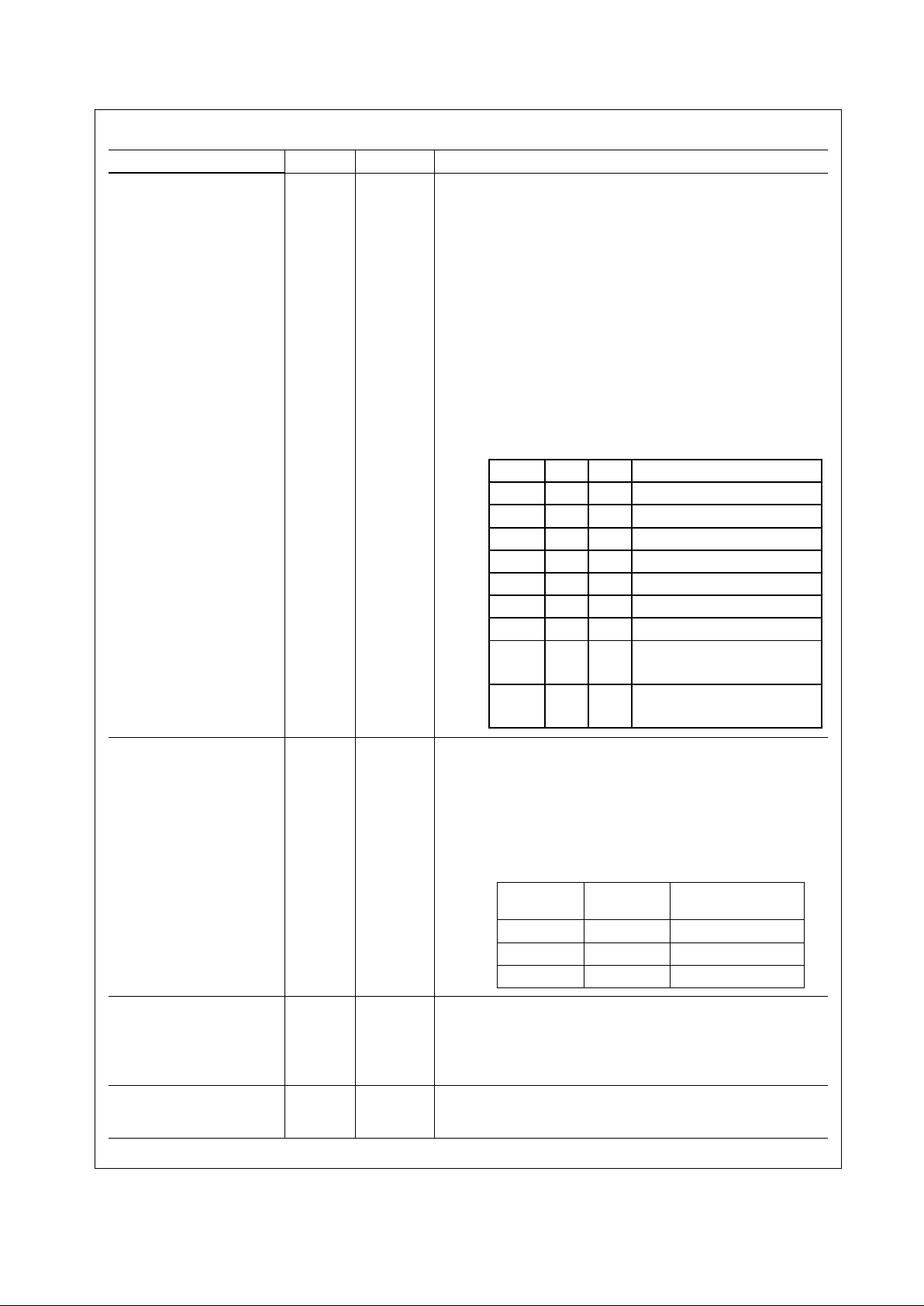
Table 1. Auto-Negotiation Modes
AN_EN AN1 AN0 Forced Mode
0 0 0 10BASE-T, Half-Duplex
0 0 1 10BASE-T, Full-Duplex
0 1 0 100BASE-TX, Half-Duplex
0 1 1 100BASE-TX, Full-Duplex
AN_EN AN1 AN0 Advertised Mode
1 0 0 10BASE-T, Half/Full-Duplex
1 0 1 100BASE-TX, Half/Full-Duplex
1 1 0 10BASE-T Half-Duplex
100BASE-TX, Half-Duplex
1 1 1 10BASE-T, Half/Full-Duplex
100BASE-TX, Half/Full-Duplex

17 www.national.com
DP83848I
ANAR. Updating the ANAR to suppress an ability is one
way for a management agent to change (restrict) the tech
-
nology that is used.
The Auto-Negotiation Link Partner Ability Register
(ANLPAR) at address 05h is used to receive the base link
code word as well as all next page code words during the
negotiati on. Furthermore, the ANLPAR will be updat ed to
either 0081h or 0021h for parallel detection to either 100
Mb/s or 10 Mb/s respectively.
The Auto-Negotiation Expansion Register (ANER) indicates additional Auto-Negotiation status. The ANER provides status on:
— Whether or not a Parallel Detect Fault has occurred
— Whether or not the Link Partne r supp orts the Next Pag e
function
— Whether or not the DP83848I supports the Next Page
function
— Whether or not the current page being exchanged by
Auto-Negotiation has been receiv ed
— Whether or not the Link Partner supports Auto-Negotia-
tion
2.1.3 Auto-Negotiation Parallel Detection
The DP83848I supports the Parallel Detection function as
defined in the IEEE 802.3u specifi ca tio n. Para lle l Detec tion
requires both the 10 Mb/s and 100 Mb/s receivers to moni
tor the receive signal and report link status to the AutoNegotiation function. Auto-Negotiation uses this informa
tion to configure th e correct t echno logy i n the e vent th at the
Link Partner does not support Auto-Negotiation but is
transmitting link signals that the 100BASE-TX or 10BASET PMAs recognize as valid link signa ls .
If the DP83848I completes Auto-Negotiation as a result of
Parallel Detection, bits 5 and 7 within the ANLPAR register
will be set to reflect the mode of operation present in the
Link Partner. Note that bits 4:0 of the ANLPAR will also be
set to 00001 based on a successful parallel detection to
indicate a valid 802.3 selector field. Software may deter
mine that negotiation completed via Parallel Detection by
reading a zero in the Link Partn er Au to-Neg oti ati on Ab le b it
once the Auto-Negotiatio n Com pl ete b it i s s et. I f co nfi gure d
for parallel detect mode and any condition other than a sin
gle good link occurs then the parallel detect fault bit will be
set.
2.1.4 Auto-Negotiation Restart
Once Auto-Negotiation has completed, it may be restarted
at any time by setting bit 9 (Res tart Auto-Negot iat ion) of the
BMCR to one. If the mode confi gured b y a su cces sful Aut oNegotiation loses a valid link, then the Auto-Negotiation
process will resume and attempt to determine the configu
ration for the link. This function ensures that a valid configuration is maintained if the cable becomes disconnected.
A renegotiation reques t fro m a ny en tity, such as a management agent, will cause the DP83848I to halt any transmit
data and link pulse activity until the break_link_timer
expires (~1500 ms). Consequently, the Link Partner will go
into link fail and normal Auto-Negotiation resumes. The
DP83848I will resume Auto-Negotiation after the
break_link_timer has expired by issuing FLP (Fast Link
Pulse) bursts.
2.1.5 Enabling Auto-Negotiation via Software
It is important to note that if the DP83848I has been initialized upon power-up as a non-auto-negotiating device
(forced technology), and it is then requ ire d that Auto-Negotiation or re-Auto-Negotiation be initiated via software,
bit
12 (Auto-Negotiation Enable) of the Basic Mode Control
Register (BMCR) must first be cleared and then set for any
Auto-Negotiation function to take effect.
2.1.6 Auto-Negotiation Complete Time
Parallel detection and Auto-Negotiation take approximately
2-3 seconds to co mp let e. In addition, Auto-Negotiatio n wi th
next page should take approximately 2-3 seconds to com
-
plete, depending on the number of next pages sent.
Refer to Clause 28 of the IEEE 802.3u standard for a full
description of the individual timers related to Auto-Negotiation.
2.2 Auto-MDIX
When enabled, this function utilizes Auto-Negotiation to
determine the proper configuration for transmission and
reception of data and subsequently selects the appropriate
MDI pair for MD I/ MD IX o per a ti on. T h e fu nc t io n us es a r an
dom seed to control switching of the crossover circuitry.
This implementati on compl ie s with the corres po ndi ng IEEE
802.3 Auto-Negotiation and Crossover Specifications.
Auto-MDIX is enabled by default and can be configu r ed vi a
strap or via PHYCR (0x19h) register, bits [15:14].
Neither Auto-Negotiation nor Auto-MDIX is required to be
enabled in forcing crossover of the MDI pairs. Forced
crossover can be achieved through the FORCE_MDIX bit,
bit 14 of PHYCR (0x19h) register.
Note: Auto-MDIX will not work in a forced mode of operation.
18 www.national.com
DP83848I
2.3 PHY Address
The 5 PHY address inputs pins are shared with the
RXD[3:0] pins and COL pin as shown below.
The DP83848I can be set to respond to any of 32 possible
PHY addresses via strap pins. The information is latched
into the PHYCR register (address 19h, bits [4:0]) at device
power-up and hardware reset. The PHY Address pins are
shared with the RXD a nd COL p ins. Ea ch DP 83848I or port
sharing an MDIO bus in a system must have a unique
physical address.
The DP83848I supports PHY Address strapping values 0
( <0000 0>) th rou gh 3 1 ( < 1 1111 > ) . St ra pp ing PHY Address
0 puts the part into Isol a t e Mod e. It should also be noted
that selecting PHY Address 0 via an MDIO write to PHYCR
will not put the device in Is olate Mode. Se e
Section 2.3.1for
more information.
For further detail relatin g to the la tch- in timi ng requi rement s
of the PHY Address pins, as well as the other hardware
configuration pins, refer to the Reset summary in
Section 6.0.
Since the PHYAD[0] pin has weak internal pull-up resistor
and PHYAD[4:1] pins have weak internal pull-down resis
tors, the default setting for the PHY address is 00001
(01h).
Refer to Figure 2 for an example o f a PHY AD c onn ec tio n to
external c omponents. In this exam ple, the PHYAD strapping results in address 00011 (03h).
2.3.1 MII Isolate Mode
The DP83848I can be put into MII Isolate mode by writing
to bit 10 of t he BMCR regi ster or by st rapping in P hysical
Address 0. It should be noted that selecting Physical
Address 0 via an MDIO write to PHYCR will not put the
device in the MII isolate mode.
When in the MII isolate mode, the DP83848I does not
respond to packet data present at TXD[3:0], TX_EN inputs
and presents a high impedance on the TX_CLK, RX_CLK,
RX_DV, RX_ER, RXD[3:0], COL, and CRS outputs. When
in Isolate mode, the DP83848I will continue to respond to
all management transactions.
While in Isolate mod e, th e PM D ou tpu t p a ir wi ll n ot t r ansm it
packet data but will continue to source 100BASE-TX
scrambled idles or 10BASE-T normal link pulses.
The DP8384 8I can Auto-Neg otiate or parallel detect to a
specific technology depending on the receive signal at the
PMD input pair. A valid link can be established for the
receiver even when the DP83848I is in Isolate mode.
Table 2. PHY Address Mapping
Pin # PHYAD Function RXD Function
42 PHYAD0 COL
43 PHYAD1 RXD_0
44 PHYAD2 RXD_1
45 PHYAD3 RXD_2
46 PHYAD4 RXD_3
Figure 2. PHYAD Strapping Example
COL
RXD_0
RXD_1
RXD_2
RXD_3
VCC
2.2kΩ
PHYAD0 = 1
PHYAD1 = 1
PHYAD2 = 0PHY AD3 = 0
PHYAD4= 0
19 www.national.com
DP83848I
2.4 LED Interface
The DP83848I supports three configurable Light Emitting
Diode (LED) pins. The device supports three LED configurations: Link, Speed, Activity and Collision. Function are
multiplexed among the LEDs. The PHY Control Register
(PHYCR) for the LEDs can also be selected through
address 19h, bits [6:5].
See Table 3 for LED Mode selection.
The LED_LINK pin in Mode 1 indicates the link status of
the port. In 100BASE-T mode, link is established as a
result of input receive amplitude compliant with the TPPMD specifications which will result in internal generation
of signal detect. A 10 Mb/s Link is est abli shed as a result of
the reception of at least seven consecutive normal Link
Pulses or the reception of a valid 10BASE-T packet. This
will cause the as se rtion of LED_LINK. LED _LINK wil l deas
sert in accordance with the Link Loss Timer as specified in
the IEEE 802.3 specification.
The LED_LINK p in in Mo de 1 w ill be OF F w h en no LI NK is
present.
The LED_LINK pin in Mode 2 and Mode 3 will be ON to
indicate Link is good and BLINK to indicate activity is
present on either transmit or receive activity.
The LED_SPEED pin indicates 10 or 100 Mb/s data rate of
the port. The standard CMOS driver goes high when operating in 100 Mb/s operation. The functionality of this LED is
independent of mode selected.
The LED_ACT/COL pin in Mode 1 indicates the presence
of either transmit or r ece iv e ac ti vit y. The LED will be ON for
Activity and OFF for No Activity. In Mode 2, this pin indi
cates the Collision status of the port. The LED will be ON
for Collision and OFF for No Collision.
The LED_ACT/COL pin in Mode 3 indicates the presence
of Duplex status for 10 Mb/s or 100 Mb/s operation. The
LED will be ON for Full Duplex and OFF for Half Duplex.
In 10 Mb/s half duplex mode, the collision LED is based on
the COL signal.
Since these LED pins are also used as strap options, the
polarity of the LED is dependent on whether the pin is
pulled up or down.
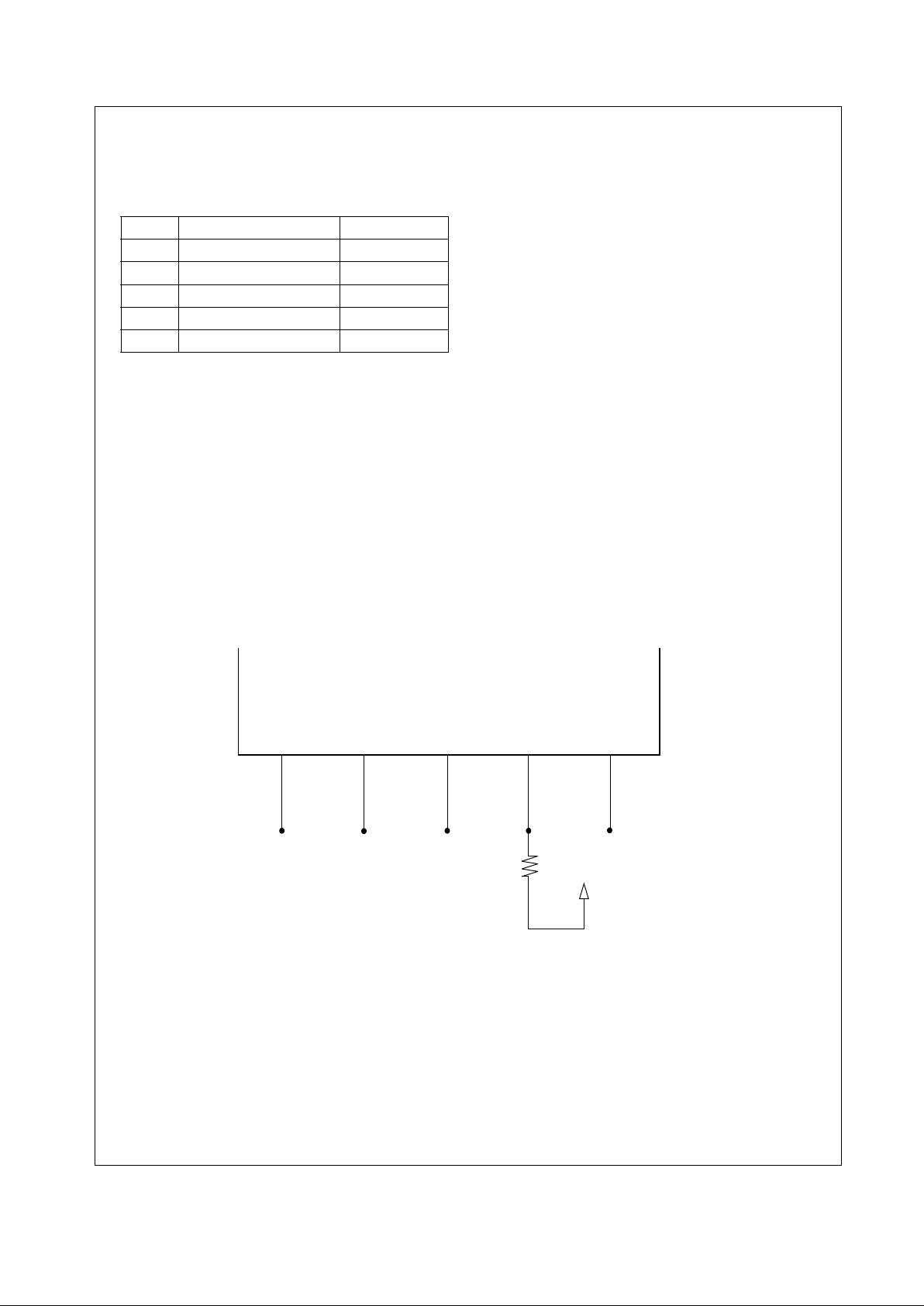
2.4.1 LEDs
Since the Auto-Negotiation (AN) strap options share the
LED output pins, the external components required for
strapping and LED usage must be considered in order to
avoid contention.
Specifically, when the LED outputs are used to drive LEDs
directly, the active state of each output driver is dependent
on the logic level sampled by the corresponding AN input
upon power-up/reset. For example, if a given AN input is
resistively pulled low then the corresponding output will be
configured as an active high driver. Conversely, if a given
AN input is resistively pulled high, then the corresponding
output will be configured as an active low driver.
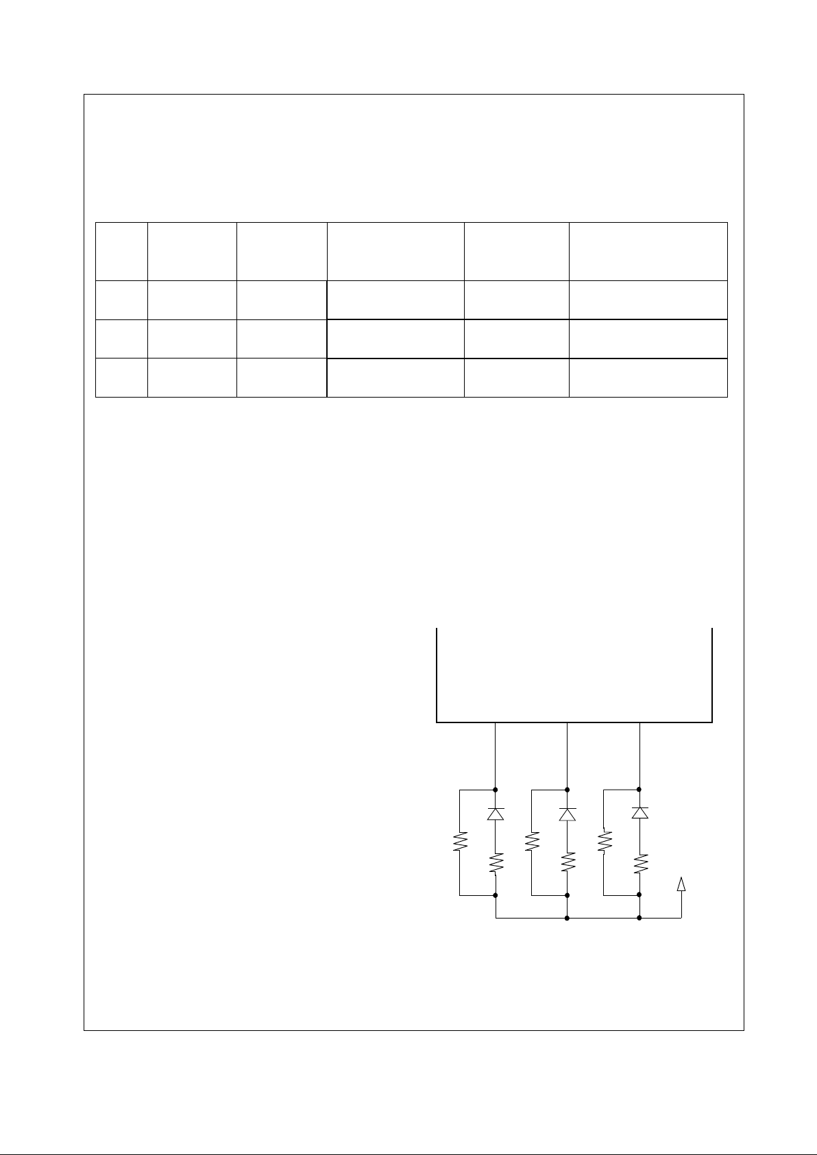
Refer to Figure 3 for an example of AN connections to
external components. In this example, the AN strapping
results in Auto-Negotiation with 10/100 Half/Full-Duplex
advertised.
The adaptive nature of the LED outputs helps to simplify
potential implemen t ation issues o f th ese dual purpos e pins .
Table 3. LED Mode Select
Mode LED_CFG[1]
(bit 6)
LED_CFG[0]
(bit 5)
or (pin40)
LED_LINK LED_SPEED LED_ACT/COL
1 don’t care 1 ON for Good Link
OFF for No Link
ON in 100 Mb/s
OFF in 10 Mb/s
ON for Activity
OFF for No Activity
2 0 0 ON for Good Link
BLINK for Activity
ON in 100 Mb/s
OFF in 10 Mb/s
ON for Collision
OFF for No Collision
3 1 0 ON for Good Link
BLINK for Activity
ON in 100 Mb/s
OFF in 10 Mb/s
ON for Full Duplex
OFF for Half Duplex
LED_LINK
LED_SPEED
LED_ACT/COL
VCC
2.2kΩ
110Ω
110Ω
2.2kΩ
110Ω
AN0 = 1
AN1 = 1
AN_EN = 1
2.2kΩ
Figure 3. AN Strapping and LED Loading Example

20 www.national.com
DP83848I
2.4.2 LED Direct Control
The DP83848I provides another option to directly control
any or all LED outputs throu gh the LED Di rect Contro l Reg
ister (LEDCR), address 18h. The register does not provide
read access to LEDs.
2.5 Half Duplex vs. Full Duplex
The DP83848I supports both half and full duplex operation
at both 10 Mb/s and 100 Mb/s speeds.
Half-duplex relies on the C SMA/C D protoc ol to ha ndle c ollisions and network access. In Half-Duplex mode, CRS
responds to both transmit and receive activity in order to
maintain compliance with the IEEE 802.3 specification.
Since the DP83848I is designed to support simultaneous
transmit and receiv e act ivi ty it is capabl e of su ppor ting full duplex switched ap plications with a throug hpu t o f up to 200
Mb/s per port when operating in 100BASE-TX mode.
Because the CSMA/CD protocol does not apply to fullduplex operation, the DP83848I disables its own internal
collision sensing and reporting functions and modifies the
behavior of Carrier Sense (CRS) such that it indicates only
receive acti vity. This allows a full-d uplex capable MAC to
operate properly.
All modes of operation (100BASE-TX and 10BASE-T) can
run either half-duplex or full-duplex. Additionally, other than
CRS and Collision reporting, all remaining MII signaling
remains the same regardless of the selected duplex mode.
It is important to understand that while Auto-Negotiation
with the use of Fast Link Pulse code words can interpret
and configure to full-duplex operation, parallel detection
can not recognize the difference between full and halfduplex from a fixed 10 Mb/s or 100 Mb/s link partner over
twisted pair. As specified in the 802.3u specification, if a
far-end link partner is configured to a forced full duplex
100BASE-TX ability, the parallel detection state machine in
the partner would be unable to detect the full duplex capa
bility of the far-end link partner. This link segment would
negotiate to a half duplex 100BASE-TX configuration
(same scenario for 10 Mb/s).
2.6 Internal Loopback
The DP83848I includes a Loopback Test mode for facilitating system diagnostics. The Loopback mode is selected
through bit 14 (Loopback) of the Basic Mode Control Reg
ister (BMCR). Writing 1 to this bit enables MII transmit data
to be routed to the MII receive outputs. Loopback status
may be checked in bit 3 of the PHY Status Register
(PHYSTS). While in Loopback mode the data will not be
transmitted onto the media. To ensure that the desired
operating mode is maintained, Auto-Negotiation should be
disabled before selecting the Loopback mode.
2.7 BIST
The DP83848I incorporates an internal Built-in Self Test
(BIST) circuit to accommodate in-circuit testing or diagnos
tics. The BIST circuit can be utilized to test the integrity of
the transmit and receive data paths. BIST testing can be
performed with the part in the internal loopback mode or
externally looped back using a loopback cable fixture.
The BIST is implemented with independent transmit and
receive paths, with the tran smit block generating a continu
ous stream of a pseudo random sequence. The user can
select a 9 bit or 15 bit pseudo random sequence from the
PSR_15 bit in the PHY Control Register (PHYCR). The
received data is compared to the generated pseudo-ran
dom data by the BIST Linear Feedback Shift Register
(LFSR) to determine the BIST pass/fail status.
The pass/fail status of the BIST is stored in the BIST status
bit in the PHYCR regis ter. The status bit defaults to 0 (BIST
fail) and will transition on a successful comparison. If an
error (mis-compare) occurs, the status bit is latched and is
cleared upon a subsequent write to the Start/Stop bit.
For transmit VOD testing, the Packet BIST Continuous
Mode can be used to allow continuous data transmission,
setting BIST_CONT_MODE, bit 5, of CDCTRL1 (0x1Bh).
The number of BIST errors can be monitored through the
BIST Error Count in the CDCTRL1 (0x1Bh), bits [15:8].

21 www.national.com
DP83848I
3.0 Functional Description
The DP83848I supports several modes of operation using
the MII interface pins. The optio ns are defi ned in th e follow
-
ing sections and include:
— MII Mode
— RMII Mode
— 10 Mb Serial Network Interface (SNI)
The modes of operation can be selected by strap options
or register control. For RMII mode, it is recommended to
use the strap option, since it requires a 50 MHz clock
instead of the normal 25 MHz.
In each of these modes, the IEEE 802.3 serial management interface is operational for device configuration and
status. The serial management interface of the MII allows
for the configuration and control of multiple PHY devices,
gathering of status, error information, and the determina
-
tion of the type and capabilities of the attached PHY(s).
3.1 MII Interface
The DP83848I incorporates the Media Independent Interface (MII) as specified in Clause 22 of the IEEE 802.3u
standard. This interface may be used to connect PHY
devices to a MAC in 10/100 Mb/s systems. This section
describes the nibble wide MII data interface.
The nibble wide MII data interface c ons is t s of a rec ei ve bus
and a transmit bus each with control signals to facilitate
data transfer between the PHY and the upper layer (MAC).
3.1.1 Nibble-wide MII Data Interface
Clause 22 of the IEEE 802.3u specification defines the
Media Independent Interface. This interface includes a
dedicated recei ve bu s an d a d edicated transmit bus . T hes e
two data buses, along with various control and status sig
nals, allow for the simultaneous exchange of data between
the DP83848I and the upper layer agent (MAC).
The receive interface consists of a nibble wide data bus
RXD[3:0], a receive error signal RX_ER, a receive data
valid flag RX_DV, and a receive clock RX_CLK for syn
chronous transfer of the data. The receive clock operates
at either 2.5 MHz to su pport 10 Mb/s operation modes or at
25 MHz to support 100 Mb/s operational modes.
The transmit interface consists of a nibble wide data bus
TXD[3:0], a transmit enable control signal TX_EN, and a
transmit cloc k TX_CL K which runs at ei ther 2. 5 MHz or 25
MHz.
Additionally, the MII includes the carrier sense signal CRS,
as well as a collision detect signal COL. The CRS signal
asserts to ind icate the re ception of d ata from the ne twork
or as a function of transmit data in Half Duplex mode. The
COL signal asse rt s as an ind ic atio n of a collision which ca n
occur during half-duplex operation when both a transmit
and receive operation occur simultaneously.
3.1.2 Collision Detect
For Half Duplex, a 10BASE-T or 100BASE-TX collision is
detected when the receive and transmit channels are
active simu ltaneously. Collisions are reported by the COL
signal on the MII.
If the DP83848I is transmitting in 10 Mb/s mode when a
collision is dete cte d, the collision is n ot r eported until seven
bits have been received while in the collision state. This
prevents a collision being reported incorrectly due to noise
on the network. The COL signal remains set for the dura
-
tion of the collision.
If a collision occ urs du ring a r eceive operation, it is i mmed i -
ately reported by the COL signal.
When heartbeat is enabled (only applicable to 10 Mb/s
operation), approximately 1µs after the transmission of
each packet, a Si gn al Q u ali ty Error (SQE) signal of approx
imately 10 bit times is generated (internally) to indicate
successful transmiss io n. SQ E is repo rted as a pul se on th e
COL signal of the MII.
3.1.3 Carrier Sense
Carrier Sense (CRS) is asserted due to receive activity,
once valid data is detected via the squelch function during
10 Mb/s operation. During 100 Mb/s operation CRS is
asserted when a valid link (SD) and two non-contiguous
zeros are detected on the line.
For 10 or 100 Mb/s Half Duple x op era tio n, C RS is a sserte d
during either packet transmission or reception.
For 10 or 100 Mb/s Full Duplex operation, CRS is asserted
only due to receive activity.
CRS is deasserted following an end of packet.
3.2 Reduced MII Interface
The DP83848I incorporates the Reduced Media Independent Interface (RMII) as specified in the RMII specification
(rev1.2) from the RMII Consortium. This interface may be
used to connect PHY devices to a MAC in 10/100 Mb/s
systems using a reduced number of pins. In this mode,
data is transferred 2-bits at a time using the 50 MHz
RMII_REF clock for both transmit and receive. The follow
ing pins are used in RMII mode:
— TX_EN
—TXD[1:0]
— RX_ER (optional for Mac)
— CRS_DV
— RXD[1:0]
— X1 (RMI I Reference c lock is 50 MHz)
In addition, the RMII mode supplies an RX_DV signal
which allows for a simpler method of recovering receive
data without having to separate RX_DV from the CRS_DV
indication. This is especially useful for systems which do
not require CRS, such as systems that only support fullduplex operation. This signal is also useful for diagnostic
testing where it may be desirable to loop Receive RMII
data directly to the transmitte r.
Since the reference clock operates at 10 times the data
rate for 10 Mb/s operation, transmit data is sampled every
10 clocks. Likewise, receive data will be generated every
10th clock so that an attached device can sample the data
every 10 clocks.
RMII mode requires a 50 MHz oscillator be connected to
the device X1 pin. A 50 MHz crystal is not supported.

22 www.national.com
DP83848I
To tolerate potential frequency differences between the 50
MHz referenc e clock an d the recove red recei ve clock, the
receive RMII function includes a programmable elasticity
buffer. The elasticity buffer is programmable to minimize
propagation delay based on expected packet size and
clock accuracy. This allows for supporting a range of
packet sizes including jumbo frames.
The elasticity buffer will force Frame Check Sequence
errors for packets which overrun or underrun the FIFO.
Underrun and Overrun conditions can be reported in the
RMII and Bypass Register (RBR). The following table indi
cates how to program the elastic ity buff er fifo (in 4-bi t increments) based on expected max packet size and clock
accuracy. It assumes both clocks (RMII Reference clock
and far-end Transmitter clock) have the same accuracy.
3.3 10 Mb Serial Network Interface (SNI)
The DP83848I incorporates a 10 Mb Serial Network Interface (SNI) which al lo ws a s im pl e ser ial d ata interface for 10
Mb only devices. This is also referred to as a 7-wire inter
face. While there is no defined standard for this interface, it
is based on early 10 Mb physical layer devices. Data is
clocked serially at 10 MHz using separate transmit and
receive paths. The following pins are used in SNI mode:
—TX_CLK
—TX_EN
—TXD[0]
—RX_CLK
—RXD[0]
— CRS
—COL
3.4 802.3u MII Serial Management Interface
3.4.1 Serial Management Register A ccess
The serial management MII specification defines a set of
thirty-two 16-bit status and control registers that are acces
sible through the management interface pins MDC and
MDIO. The DP83848I implements all the required MII reg
isters as well as several optional registers. These registers
are fully described in
Section 7.0. A description of the seria l
management access protocol follows.
3.4.2 Serial Management Access Protocol
The serial cont rol interface co nsists of two pins, Management Data Clock (MDC) and Management Data Input/Output (MDIO). MDC has a maximum clock rate of 25 MHz
and no minimum rate. The MDIO line is bi-directional and
may be shared by up to 32 devices. The MDIO frame for
mat is shown below in Table 5.
The MDIO pin requires a pull-up resistor (1.5 kΩ) which,
during IDLE and turnaro und, will pull M DIO hi gh. In o rder to
initialize the MDIO int erface , the st atio n manag ement entit y
sends a sequence of 32 contiguous logic ones on MDIO to
provide the DP83848I with a sequence that can be used to
establish synchronization. This preamble may be gener
ated either by driving MDIO high for 32 consecutive MDC
clock cycles, or by simply allowing the MDIO pull-up resis
tor to pull the MDIO pin high during which time 32 MDC
clock cycles are provided. In addition 32 MDC clock cycles
should be used to re-sync the device if an invalid start,
opcode, or turnaround bit is detected.
The DP83848I waits until it has received this preamble
sequence before responding to any other transaction.
Once the DP83848I serial management port has been ini
tialized no further preamble sequencing is required until
after a power-on/reset, invalid Start, invalid Opcode, or
invalid turnaround bit has occurred.
The St art co de is in dic ate d by a <01> p atte rn. Th is ass ure s
the MDIO line transitions from the default idle line state.
Turnaround is defined as an idle bit time inserted between
the Register Address field and the Data field. To avoid contention during a read transaction, no device shall actively
drive the MDIO signal during the first bit of Turnaround.
The addressed DP83848I drives the MDIO with a zero for
the second bit of turnaround and follows this with the
required data.
Figure 4 shows the timing relationship
between MDC and th e MDIO as dr iven/re ceived by the Station (STA) and the DP83848I (PHY) for a typical register
read access.
For write transactions, the station management entity
writes data to the addresse d DP838 48I thus eli mina ting the
requirement for MDIO Turnaround. The Turnaround time is
filled by the management entity by inserting <10>.
Figure 5
shows the timing relationship for a typical MII register write
access.
Table 4. Supported packet sizes at +/-50ppm +/-100ppm for each clock
Start Threshold
RBR[1:0]
Latency Tolerance Recommende d Packet Size
at +/- 50ppm
Recommended Packet Size
at +/- 100ppm
1 (4-bits) 2 bits 24 00 byt es 1200 bytes
2 (8-bits) 6 bits 72 00 byt es 3600 bytes
3 (12-bits) 10 bits 12000 bytes 6000 bytes
0 (16-bits) 14 bits 16800 bytes 8400 bytes
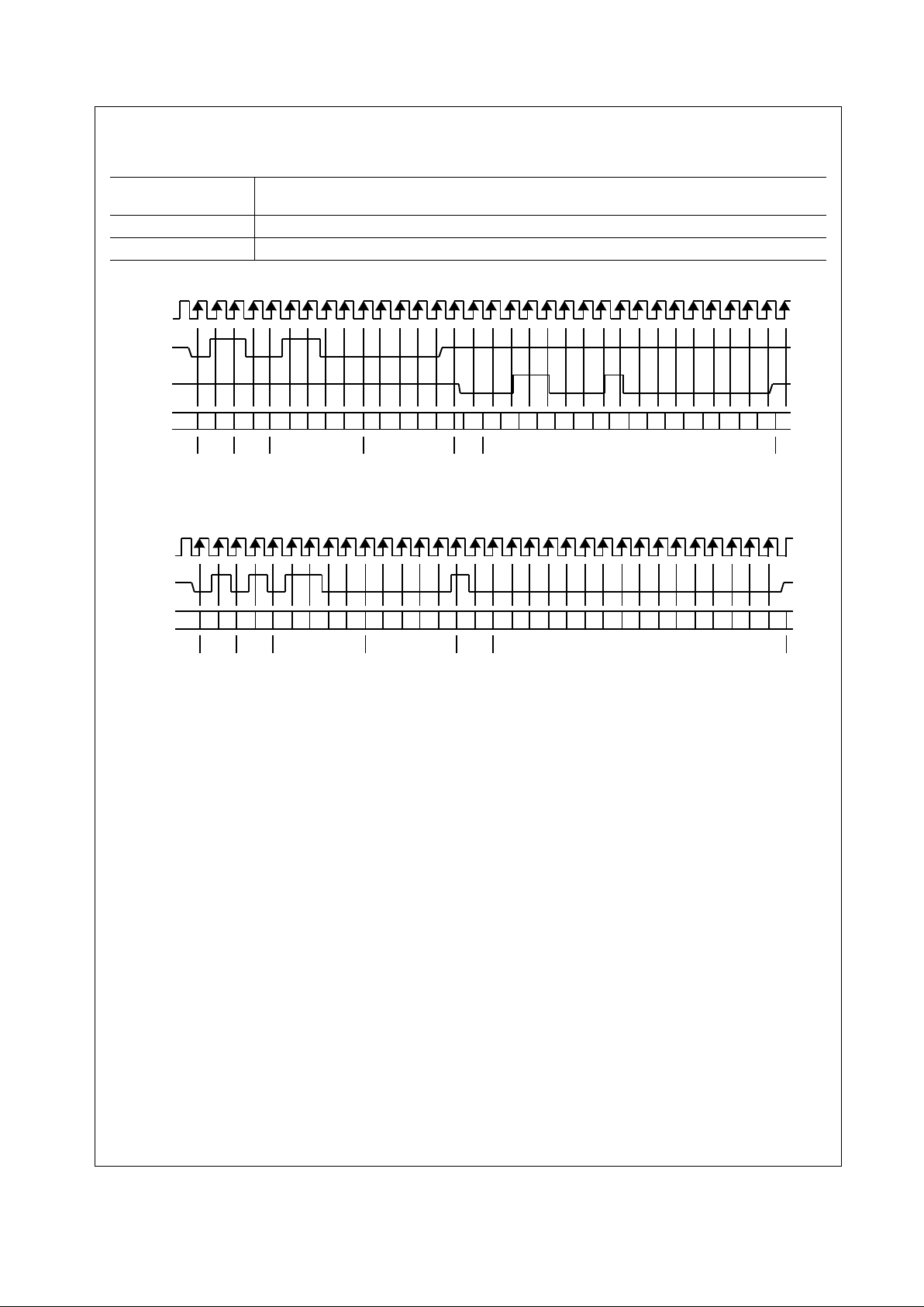
23 www.national.com
DP83848I
3.4.3 Serial Management Preamble Suppression
The DP83848I supports a Preamble Suppression mode as
indicated by a one in bit 6 of the Basic Mode Status Regis
ter (BMSR, address 01h.) If the station management entity
(i.e. MAC or other management controller) determines that
all PHYs in the system support Preamble Suppression by
returning a one in this bit, then the station management
entity need not generate preamble for each management
transaction.
The DP83848I requires a single initialization sequence of
32 bits of preamble fol lo w ing hard ware/s oftware reset. This
requirement is generally met by the mandatory pull-up
resistor on MDI O in co nj u nc tio n wi th a co nt i nuo u s MD C, or
the management access made to determine whether Pre
-
amble Suppression is supported.
While the DP83848I requires an initial preamble sequence
of 32 bits for management initialization, it does not require
a full 32-bit sequence between each subsequent transac
tion. A minimum of one idle bit between management
transactions is required as specified in the IEEE 802.3u
specification.
Table 5. Typical MDIO Frame Format
MII Management
Serial Protocol
<idle><start><op code><device addr><reg addr><turnaround><data><idle>
Read Operation <idle><01><10><AAAAA><RRRRR><Z0><xxxx xxxx xxxx xxxx><idle>
Write Operation <idle><01><01><AAAAA><RRRRR><10><xxxx xxxx xxxx xxxx><idle>
Figure 4. Typical MDC/MDIO Read Operation
Figure 5. Typical MDC/MDIO Write Operation
MDC
MDIO
00011 110000000
(STA)
Idle Start
Opcode
(Read)
PHY Address
(PHYAD = 0Ch)
Register Address
(00h = BMCR)
TA
Register Data
Z
MDIO
(PHY)
Z
Z
Z
0 0 011000100000000
Z
Idle
Z
Z
MDC
MDIO
00011110000000
(STA)
Idle Start
Opcode
(Write)
PHY Address
(PHYAD = 0Ch)
Register Address
(00h = BMCR)
TA
Register Data
Z
0 0 0 000 00000000
Z
Idle
1000
ZZ
24 www.national.com
DP83848I
4.0 Architecture
This section describes the operations within each transceiver module, 100BASE-TX and 10BASE-T. Each operation consists of several functional blocks and described in
the following:
— 100BASE-TX Transmitter
— 100BASE-TX Receiver
— 10BASE-T Transceiver Module
4.1 100BASE-TX TRANSMITTER
The 100BASE-TX transmitter consists of several functional
blocks which conver t sync hronous 4-bit ni bble d at a, as p ro
vided by the MII, to a scrambled MLT-3 125 Mb/s serial
data stream. Because the 100BASE-TX TP-PMD is integrated, the differential output pins, PMD Output Pair, can
be directly routed to the magnetics.
The block diagram in Figure 6. provides an overview of
each functional block within the 100BASE-TX transmit section.
The Transmitter section consists of the following functional
blocks:
— Code-group Encoder and Injection block
— Scrambler block (bypass option)
— NRZ to NRZI encoder block
— Binary to MLT-3 converter / Common Driver
The bypass option for the functional blocks within the
100BASE-TX transmitter provides flexibility for applications
where data conversion is not always required. The
DP83848I implements the 100BASE-TX transmit state
machine diagram as specified in the IEEE 802.3u Stan
-
dard, Clause 24.
Figure 6. 100BASE-TX Transmit Block Diagram
4B5B CODE-
GROUP
ENCODER &
SCRAMBLER
NRZ TO NRZI
ENCODER
5B PARALLEL
TO SERIAL
PMD OUTPUT PAIR
TX_CLK
TXD[3:0] /
TX_EN
BINARY
TO MLT-3 /
COMMON
DRIVER
125MHZ CLOCK
BP_SCR
MUX
100BASE-TX
LOOPBACK
MLT[1:0]
DIVIDE
BY 5

25 www.national.com
DP83848I
Table 5. 4B5B CCode-group Encoding and Injection
The code-group encoder converts 4-bit (4B) nibble data
generated by the MAC into 5-bit (5B) code-groups for
transmission. This conversion is required to allow control
data to be combined with packet data code-groups. Refer
to
Table 5 for 4B to 5B code-group mapping details.
The code-group encoder substitutes the first 8-bits of the
MAC preamble with a J/K code-group pair (11000 10001)
upon transmission. The code-group encoder continues to
replace subsequent 4B preamble and data nibbles with
corresponding 5B code-groups. At the end of the transmit
packet, upon the deassertion of Transmit Enable signal
from the MAC, the code-group encoder injects the T/R
code-group pair (01101 00111) indicating the end of the
frame.
After the T/R code-group pair, the code-group encoder
continuously injects IDLEs into the transmit data stream
until the next transmit packet is detected (reassertion of
Transmit Enable).
4.1.1 Scrambler
The scrambler is required to control the radiated emissions
at the media connector and on the twisted pair cable (for
DATA CODES
0 11110 0000
1 01001 0001
2 10100 0010
3 10101 0011
4 01010 0100
5 01011 0101
6 01110 0110
7 01111 0111
8 10010 1000
9 10011 1001
A 10110 1010
B 10111 1011
C 11010 1100
D 11011 1101
E 11100 1110
F 11101 1111
IDLE AND CONTROL CODES
H 00100 HALT code-group - Error code
I 11111 Inter-Packet IDLE - 0000 (Note 1)
J 11000 First Start of Packet - 0101 (Note 1)
K 10001 Second Start of Packet - 0101 (Note 1)
T 01101 First End of Packet - 0000 (Note 1)
R 00111 Second End of Packet - 0000 (Note 1)
INVALID CODES
V 00000
V 00001
V 00010
V 00011
V 00101
V 00110
V 01000
V 01100
Note: Control code-groups I, J, K, T and R in data fields will be mapped as invalid codes, together with RX_ER asserted.
6.
 Loading...