

© 2007 National Semiconductor Corporation www.national.com
1
DP83848C PHYTER
®
— Commercial Temperature Single Port 10/100 Mb/s Ethernet Physical Layer Transceiver
Febuary 2007
DP83848C PHYTER® - Commercial Temperature
Single Port 10/100 Mb/s Ethernet Physical Layer Transceiver
General Description
The DP83848C is a robust fully featured 10/100 single
port Physical Layer device offering low power consumption, including several intelligent power down
states. These low power modes increase overall product reliability due to decre ased powe r dissi pat ion. Supporting multiple intelligent power modes allows the
application to use the absolute minimum amount of
power needed for operation.
The DP83848C includes a 25MHz clock out. This
means that the application can be designed with a
minimum of external parts, which in turn results in the
lowest possible total cost of the solution.
The DP83848C easily interfaces to twisted pair media
via an external transformer. Both MII and RMII are
supported ensuring ease and flexibility of design.
The DP83848C features integrated sublayers to support both 10BASE-T and 100BASE-TX Ethernet pro tocols, which ensures compatibility and interoperability
with all other standards based Ethernet solutions.
The DP83848C is offered in a small form factor (48 pi n
LQFP) so that a minimum of board space is needed.
Applications
• High End Peripheral Devices
• Industrial Controls and Factory Automation
• General Embedded Applications
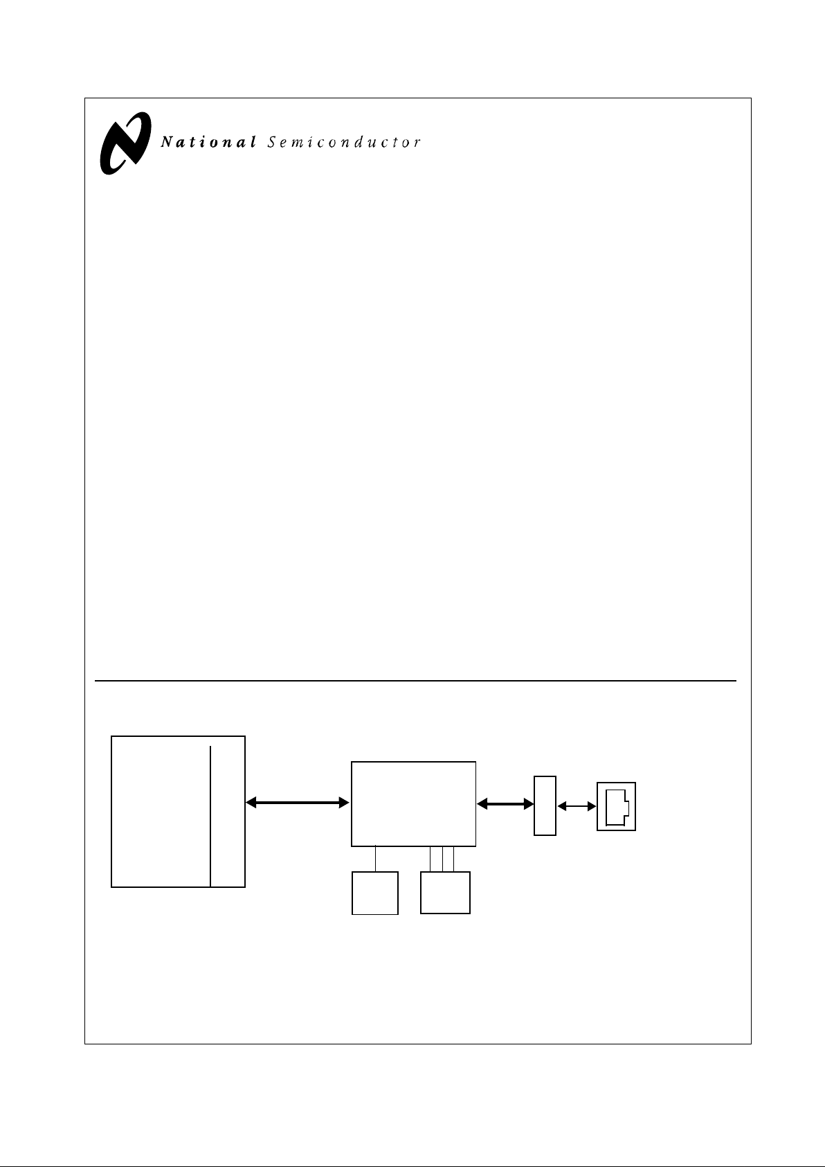
System Diagram
PHYTER® is a registered trademark of National Semiconductor.
Status
10BASE-T
or
100BASE-TX
MII/RMII/SNI
25 MHz
Magnetics
RJ-45
Clock
LEDs
DP83848C
10/100 Mb/s
Media Access Controller
MPU/CPU
Source
Typical Application
Features
• Low-power 3.3V, 0.18µm CMOS technology
• Low power consumption < 270mW Typical
• 3.3V MAC Interface
• Auto-MDIX for 10/100 Mb/s
• Energy Detection Mode
• 25 MHz clock out
• SNI Interface (configurable)
• RMII Rev. 1.2 Interface (configurable)
• MII Serial Management Interface (MDC and MDIO)
• IEEE 802.3u MII
• IEEE 802.3u Auto-Negotiation and Parallel Detection
• IEEE 802.3u ENDEC, 10BASE-T transceivers and filters
• IEEE 802.3u PCS, 100BASE-TX transceivers and filters
• Integrated ANSI X3.263 compliant TP-PMD physical sub-
layer with adaptive equalization and Baseline Wander compensation
• Error-free Operation up to 137 meters
• Programmable LED support Link, 10 /100 Mb/s Mode, Activ-
ity, and Collision Detect
• Single register access for complete PHY status
• 10/100 Mb/s packet BIST (Built in Self Test)
• 48-pin LQFP package (7mm) x (7mm)
2 www.national.com
DP83848C
SERIAL
MANAGEMENT
TX_CLK
TXD[3:0]
TX_EN
MDIO
MDC
COL
CRS/CRS_DV
RX_ER
RX_DV
RXD[3:0]
RX_CLK
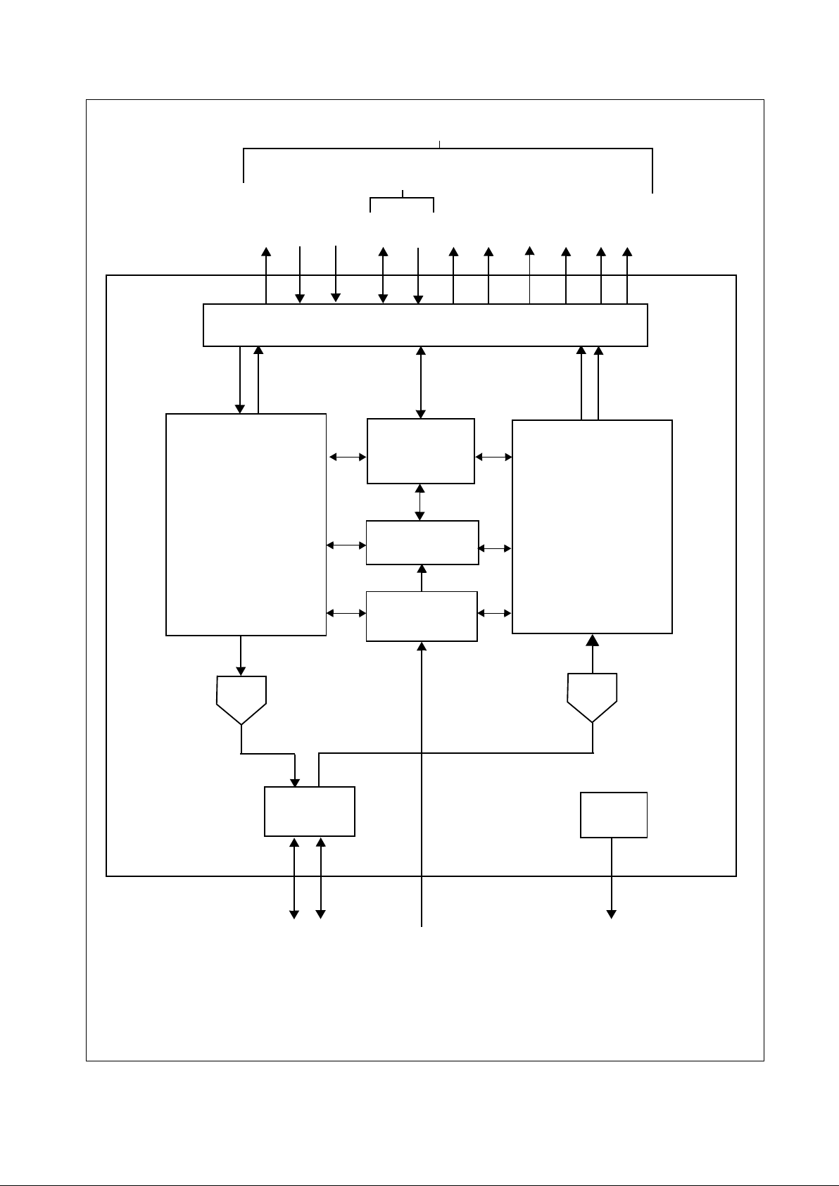
Auto-Negotiation
State Machine
Clock
RX_DATA
RX_CLK
TX_DATA TX_CLK
REFERENCE CLOCK
TD±
RD±
LEDS
Generation
MII/RMII/SNI INTERFACES
Figure 1. DP83848C Functional Block Diagram
MII
Registers
Transmit
Block
10BASE-T &
100BASE-TX
10BASE-T &
100BASE-TX
Receive
Block
Auto-MDIX
DAC
ADC
LED
Drivers
MII/RMII/SNI

3 www.national.com
DP83848C
Table of Contents
1.0 Pin Descriptions . . . . . . . . . . . . . . . . . . . . . . . . . . . . . . . . . . . . . . . . . . . . . . . . . 9
1.1 Serial Management Interface . . . . . . . . . . . . . . . . . . . . . . . . . . . . . . . . . . . . . . . . . . . . . . .9
1.2 MAC Data Interface . . . . . . . . . . . . . . . . . . . . . . . . . . . . . . . . . . . . . . . . . . . . . . . . . . . . . .9
1.3 Clock Interface . . . . . . . . . . . . . . . . . . . . . . . . . . . . . . . . . . . . . . . . . . . . . . . . . . . . . . . . .11
1.4 LED Interface . . . . . . . . . . . . . . . . . . . . . . . . . . . . . . . . . . . . . . . . . . . . . . . . . . . . . . . . . .11
1.5 Reset and Power Down . . . . . . . . . . . . . . . . . . . . . . . . . . . . . . . . . . . . . . . . . . . . . . . . . .12
1.6 Strap Options . . . . . . . . . . . . . . . . . . . . . . . . . . . . . . . . . . . . . . . . . . . . . . . . . . . . . . . . . .12
1.7 10 Mb/s and 100 Mb/s PMD Interface . . . . . . . . . . . . . . . . . . . . . . . . . . . . . . . . . . . . . . .14
1.8 Special Connections . . . . . . . . . . . . . . . . . . . . . . . . . . . . . . . . . . . . . . . . . . . . . . . . . . . . .14
1.9 Power Supply Pins . . . . . . . . . . . . . . . . . . . . . . . . . . . . . . . . . . . . . . . . . . . . . . . . . . . . . .14
1.10 Package Pin Assignments . . . . . . . . . . . . . . . . . . . . . . . . . . . . . . . . . . . . . . . . . . . . . . .15
2.0 Configuration . . . . . . . . . . . . . . . . . . . . . . . . . . . . . . . . . . . . . . . . . . . . . . . . . . 16
2.1 Auto-Negotiation . . . . . . . . . . . . . . . . . . . . . . . . . . . . . . . . . . . . . . . . . . . . . . . . . . . . . . . .16
2.1.1 Auto-Negotiation Pin Control . . . . . . . . . . . . . . . . . . . . . . . . . . . . . . . . . . . . . . . . . . . . . . . . . 16
2.1.2 Auto-Negotiation Register Control . . . . . . . . . . . . . . . . . . . . . . . . . . . . . . . . . . . . . . . . . . . . . 16
2.1.3 Auto-Negotiation Parallel Detection . . . . . . . . . . . . . . . . . . . . . . . . . . . . . . . . . . . . . . . . . . . . 17
2.1.4 Auto-Negotiation Restart . . . . . . . . . . . . . . . . . . . . . . . . . . . . . . . . . . . . . . . . . . . . . . . . . . . . 17
2.1.5 Enabling Auto-Negotiation via Software . . . . . . . . . . . . . . . . . . . . . . . . . . . . . . . . . . . . . . . . 17
2.1.6 Auto-Negotiation Complete Time . . . . . . . . . . . . . . . . . . . . . . . . . . . . . . . . . . . . . . . . . . . . . . 17
2.2 Auto-MDIX . . . . . . . . . . . . . . . . . . . . . . . . . . . . . . . . . . . . . . . . . . . . . . . . . . . . . . . . . . . .17
2.3 PHY Address . . . . . . . . . . . . . . . . . . . . . . . . . . . . . . . . . . . . . . . . . . . . . . . . . . . . . . . . . .18
2.3.1 MII Isolate Mode . . . . . . . . . . . . . . . . . . . . . . . . . . . . . . . . . . . . . . . . . . . . . . . . . . . . . . . . . . 18
2.4 LED Interface . . . . . . . . . . . . . . . . . . . . . . . . . . . . . . . . . . . . . . . . . . . . . . . . . . . . . . . . . .19
2.4.1 LEDs . . . . . . . . . . . . . . . . . . . . . . . . . . . . . . . . . . . . . . . . . . . . . . . . . . . . . . . . . . . . . . . . . . . 19
2.4.2 LED Direct Control . . . . . . . . . . . . . . . . . . . . . . . . . . . . . . . . . . . . . . . . . . . . . . . . . . . . . . . . . 20
2.5 Half Duplex vs. Full Duplex . . . . . . . . . . . . . . . . . . . . . . . . . . . . . . . . . . . . . . . . . . . . . . .20
2.6 Internal Loopback . . . . . . . . . . . . . . . . . . . . . . . . . . . . . . . . . . . . . . . . . . . . . . . . . . . . . . .20
2.7 BIST . . . . . . . . . . . . . . . . . . . . . . . . . . . . . . . . . . . . . . . . . . . . . . . . . . . . . . . . . . . . . . . . .20
3.0 Functional Description. . . . . . . . . . . . . . . . . . . . . . . . . . . . . . . . . . . . . . . . . . . 21
3.1 MII Interface . . . . . . . . . . . . . . . . . . . . . . . . . . . . . . . . . . . . . . . . . . . . . . . . . . . . . . . . . . .21
3.1.1 Nibble-wide MII Data Interface . . . . . . . . . . . . . . . . . . . . . . . . . . . . . . . . . . . . . . . . . . . . . . . . 21
3.1.2 Collision Detect . . . . . . . . . . . . . . . . . . . . . . . . . . . . . . . . . . . . . . . . . . . . . . . . . . . . . . . . . . . 21
3.1.3 Carrier Sense . . . . . . . . . . . . . . . . . . . . . . . . . . . . . . . . . . . . . . . . . . . . . . . . . . . . . . . . . . . . . 21
3.2 Reduced MII Interface . . . . . . . . . . . . . . . . . . . . . . . . . . . . . . . . . . . . . . . . . . . . . . . . . . .21
3.3 10 Mb Serial Network Interface (SNI) . . . . . . . . . . . . . . . . . . . . . . . . . . . . . . . . . . . . . . . .22
3.4 802.3u MII Serial Management Interface . . . . . . . . . . . . . . . . . . . . . . . . . . . . . . . . . . . . .22
3.4.1 Serial Management Register Access . . . . . . . . . . . . . . . . . . . . . . . . . . . . . . . . . . . . . . . . . . . 22
3.4.2 Serial Management Access Protocol . . . . . . . . . . . . . . . . . . . . . . . . . . . . . . . . . . . . . . . . . . . 22
3.4.3 Serial Management Preamble Suppression . . . . . . . . . . . . . . . . . . . . . . . . . . . . . . . . . . . . . 23
4.0 Architecture. . . . . . . . . . . . . . . . . . . . . . . . . . . . . . . . . . . . . . . . . . . . . . . . . . . . 24
4.1 100BASE-TX TRANSMITTER . . . . . . . . . . . . . . . . . . . . . . . . . . . . . . . . . . . . . . . . . . . . .24
4.1.1 Code-group Encoding and Injection . . . . . . . . . . . . . . . . . . . . . . . . . . . . . . . . . . . . . . . . . . . . 26
4.1.2 Scrambler . . . . . . . . . . . . . . . . . . . . . . . . . . . . . . . . . . . . . . . . . . . . . . . . . . . . . . . . . . . . . . . . 26
4.1.3 NRZ to NRZI Encoder . . . . . . . . . . . . . . . . . . . . . . . . . . . . . . . . . . . . . . . . . . . . . . . . . . . . . . 26
4.1.4 Binary to MLT-3 Convertor . . . . . . . . . . . . . . . . . . . . . . . . . . . . . . . . . . . . . . . . . . . . . . . . . . . 26
4.2 100BASE-TX RECEIVER . . . . . . . . . . . . . . . . . . . . . . . . . . . . . . . . . . . . . . . . . . . . . . . . .26
4.2.1 Analog Front End . . . . . . . . . . . . . . . . . . . . . . . . . . . . . . . . . . . . . . . . . . . . . . . . . . . . . . . . . . 26
4.2.2 Digital Signal Processor . . . . . . . . . . . . . . . . . . . . . . . . . . . . . . . . . . . . . . . . . . . . . . . . . . . . . 26
4.2.2.1 Digital Adaptive Equalization and Gain Control . . . . . . . . . . . . . . . . . . . . . . . . . . . . . . 28
4.2.2.2 Base Line Wander Compensation . . . . . . . . . . . . . . . . . . . . . . . . . . . . . . . . . . . . . . . . 29
4.2.3 Signal Detect . . . . . . . . . . . . . . . . . . . . . . . . . . . . . . . . . . . . . . . . . . . . . . . . . . . . . . . . . . . . . 29
4.2.4 MLT-3 to NRZI Decoder . . . . . . . . . . . . . . . . . . . . . . . . . . . . . . . . . . . . . . . . . . . . . . . . . . . . . 29
4.2.5 NRZI to NRZ . . . . . . . . . . . . . . . . . . . . . . . . . . . . . . . . . . . . . . . . . . . . . . . . . . . . . . . . . . . . . 29
4.2.6 Serial to Parallel . . . . . . . . . . . . . . . . . . . . . . . . . . . . . . . . . . . . . . . . . . . . . . . . . . . . . . . . . . . 29
4.2.7 Descrambler . . . . . . . . . . . . . . . . . . . . . . . . . . . . . . . . . . . . . . . . . . . . . . . . . . . . . . . . . . . . . . 30
4.2.8 Code-group Alignment . . . . . . . . . . . . . . . . . . . . . . . . . . . . . . . . . . . . . . . . . . . . . . . . . . . . . . 30

4 www.national.com
DP83848C
4.2.9 4B/5B Decoder . . . . . . . . . . . . . . . . . . . . . . . . . . . . . . . . . . . . . . . . . . . . . . . . . . . . . . . . . . . . 30
4.2.10 100BASE-TX Link Integrity Monitor . . . . . . . . . . . . . . . . . . . . . . . . . . . . . . . . . . . . . . . . . . . 30
4.2.11 Bad SSD Detection . . . . . . . . . . . . . . . . . . . . . . . . . . . . . . . . . . . . . . . . . . . . . . . . . . . . . . . 30
4.3 10BASE-T TRANSCEIVER MODULE . . . . . . . . . . . . . . . . . . . . . . . . . . . . . . . . . . . . . . .30
4.3.1 Operational Modes . . . . . . . . . . . . . . . . . . . . . . . . . . . . . . . . . . . . . . . . . . . . . . . . . . . . . . . . . 30
4.3.2 Smart Squelch . . . . . . . . . . . . . . . . . . . . . . . . . . . . . . . . . . . . . . . . . . . . . . . . . . . . . . . . . . . . 31
4.3.3 Collision Detection and SQE . . . . . . . . . . . . . . . . . . . . . . . . . . . . . . . . . . . . . . . . . . . . . . . . . 31
4.3.4 Carrier Sense . . . . . . . . . . . . . . . . . . . . . . . . . . . . . . . . . . . . . . . . . . . . . . . . . . . . . . . . . . . . . 31
4.3.5 Normal Link Pulse Detection/Generation . . . . . . . . . . . . . . . . . . . . . . . . . . . . . . . . . . . . . . . . 31
4.3.6 Jabber Function . . . . . . . . . . . . . . . . . . . . . . . . . . . . . . . . . . . . . . . . . . . . . . . . . . . . . . . . . . . 32
4.3.7 Automatic Link Polarity Detection and Correction . . . . . . . . . . . . . . . . . . . . . . . . . . . . . . . . . 32
4.3.8 Transmit and Receive Filtering . . . . . . . . . . . . . . . . . . . . . . . . . . . . . . . . . . . . . . . . . . . . . . . 32
4.3.9 Transmitter . . . . . . . . . . . . . . . . . . . . . . . . . . . . . . . . . . . . . . . . . . . . . . . . . . . . . . . . . . . . . . . 32
4.3.10 Receiver . . . . . . . . . . . . . . . . . . . . . . . . . . . . . . . . . . . . . . . . . . . . . . . . . . . . . . . . . . . . . . . . 32
5.0 Design Guidelines. . . . . . . . . . . . . . . . . . . . . . . . . . . . . . . . . . . . . . . . . . . . . . . 33
5.1 TPI Network Circuit . . . . . . . . . . . . . . . . . . . . . . . . . . . . . . . . . . . . . . . . . . . . . . . . . . . . . .33
5.2 ESD Protection . . . . . . . . . . . . . . . . . . . . . . . . . . . . . . . . . . . . . . . . . . . . . . . . . . . . . . . . .34
5.3 Clock In (X1) Requirements . . . . . . . . . . . . . . . . . . . . . . . . . . . . . . . . . . . . . . . . . . . . . . .34
5.4 Power Feedback Circuit . . . . . . . . . . . . . . . . . . . . . . . . . . . . . . . . . . . . . . . . . . . . . . . . . .35
5.5 Power Down/Interrupt . . . . . . . . . . . . . . . . . . . . . . . . . . . . . . . . . . . . . . . . . . . . . . . . . . . .35
5.5.1 Power Down Control Mode . . . . . . . . . . . . . . . . . . . . . . . . . . . . . . . . . . . . . . . . . . . . . . . . . . 35
5.5.2 Interrupt Mechanisms . . . . . . . . . . . . . . . . . . . . . . . . . . . . . . . . . . . . . . . . . . . . . . . . . . . . . . 35
5.6 Energy Detect Mode . . . . . . . . . . . . . . . . . . . . . . . . . . . . . . . . . . . . . . . . . . . . . . . . . . . . .35
6.0 Reset Operation . . . . . . . . . . . . . . . . . . . . . . . . . . . . . . . . . . . . . . . . . . . . . . . . 36
6.1 Hardware Reset . . . . . . . . . . . . . . . . . . . . . . . . . . . . . . . . . . . . . . . . . . . . . . . . . . . . . . . .36
6.2 Software Reset . . . . . . . . . . . . . . . . . . . . . . . . . . . . . . . . . . . . . . . . . . . . . . . . . . . . . . . . .36
7.0 Register Block . . . . . . . . . . . . . . . . . . . . . . . . . . . . . . . . . . . . . . . . . . . . . . . . . 37
7.1 Register Definition . . . . . . . . . . . . . . . . . . . . . . . . . . . . . . . . . . . . . . . . . . . . . . . . . . . . . .40
7.1.1 Basic Mode Control Register (BMCR) . . . . . . . . . . . . . . . . . . . . . . . . . . . . . . . . . . . . . . . . . . 41
7.1.2 Basic Mode Status Register (BMSR) . . . . . . . . . . . . . . . . . . . . . . . . . . . . . . . . . . . . . . . . . . . 43
7.1.3 PHY Identifier Register #1 (PHYIDR1) . . . . . . . . . . . . . . . . . . . . . . . . . . . . . . . . . . . . . . . . . . 44
7.1.4 PHY Identifier Register #2 (PHYIDR2) . . . . . . . . . . . . . . . . . . . . . . . . . . . . . . . . . . . . . . . . . . 44
7.1.5 Auto-Negotiation Advertisement Register (ANAR) . . . . . . . . . . . . . . . . . . . . . . . . . . . . . . . . . 44
7.1.6 Auto-Negotiation Link Partner Ability Register (ANLPAR) (BASE Page) . . . . . . . . . . . . . . . . 46
7.1.7 Auto-Negotiation Link Partner Ability Register (ANLPAR) (Next Page) . . . . . . . . . . . . . . . . . 47
7.1.8 Auto-Negotiate Expansion Register (ANER) . . . . . . . . . . . . . . . . . . . . . . . . . . . . . . . . . . . . . 47
7.1.9 Auto-Negotiation Next Page Transmit Register (ANNPTR) . . . . . . . . . . . . . . . . . . . . . . . . . . 48
7.2 Extended Registers . . . . . . . . . . . . . . . . . . . . . . . . . . . . . . . . . . . . . . . . . . . . . . . . . . . . .49
7.2.1 PHY Status Register (PHYSTS) . . . . . . . . . . . . . . . . . . . . . . . . . . . . . . . . . . . . . . . . . . . . . . 49
7.2.2 MII Interrupt Control Register (MICR) . . . . . . . . . . . . . . . . . . . . . . . . . . . . . . . . . . . . . . . . . . 51
7.2.3 MII Interrupt Status and Misc. Control Register (MISR) . . . . . . . . . . . . . . . . . . . . . . . . . . . . . 52
7.2.4 False Carrier Sense Counter Register (FCSCR) . . . . . . . . . . . . . . . . . . . . . . . . . . . . . . . . . . 53
7.2.5 Receiver Error Counter Register (RECR) . . . . . . . . . . . . . . . . . . . . . . . . . . . . . . . . . . . . . . . 53
7.2.6 100 Mb/s PCS Configuration and Status Register (PCSR) . . . . . . . . . . . . . . . . . . . . . . . . . . 54
7.2.7 RMII and Bypass Register (RBR) . . . . . . . . . . . . . . . . . . . . . . . . . . . . . . . . . . . . . . . . . . . . . 55
7.2.8 LED Direct Control Register (LEDCR) . . . . . . . . . . . . . . . . . . . . . . . . . . . . . . . . . . . . . . . . . . 55
7.2.9 PHY Control Register (PHYCR) . . . . . . . . . . . . . . . . . . . . . . . . . . . . . . . . . . . . . . . . . . . . . . . 56
7.2.10 10Base-T Status/Control Register (10BTSCR) . . . . . . . . . . . . . . . . . . . . . . . . . . . . . . . . . . 57
7.2.11 CD Test and BIST Extensions Register (CDCTRL1) . . . . . . . . . . . . . . . . . . . . . . . . . . . . . . 59
7.2.12 Energy Detect Control (EDCR) . . . . . . . . . . . . . . . . . . . . . . . . . . . . . . . . . . . . . . . . . . . . . . 60
8.0 Electrical Specifications. . . . . . . . . . . . . . . . . . . . . . . . . . . . . . . . . . . . . . . . . . 61
8.1 DC Specs . . . . . . . . . . . . . . . . . . . . . . . . . . . . . . . . . . . . . . . . . . . . . . . . . . . . . . . . . . . . .61
8.2 AC Specs . . . . . . . . . . . . . . . . . . . . . . . . . . . . . . . . . . . . . . . . . . . . . . . . . . . . . . . . . . . . .63
8.2.1 Power Up Timing . . . . . . . . . . . . . . . . . . . . . . . . . . . . . . . . . . . . . . . . . . . . . . . . . . . . . . . . . . 63
8.2.2 Reset Timing . . . . . . . . . . . . . . . . . . . . . . . . . . . . . . . . . . . . . . . . . . . . . . . . . . . . . . . . . . . . . 64
8.2.3 MII Serial Management Timing . . . . . . . . . . . . . . . . . . . . . . . . . . . . . . . . . . . . . . . . . . . . . . . 65
8.2.4 100 Mb/s MII Transmit Timing . . . . . . . . . . . . . . . . . . . . . . . . . . . . . . . . . . . . . . . . . . . . . . . . 65
8.2.5 100 Mb/s MII Receive Timing . . . . . . . . . . . . . . . . . . . . . . . . . . . . . . . . . . . . . . . . . . . . . . . . 66
8.2.6 100BASE-TX Transmit Packet Latency Timing . . . . . . . . . . . . . . . . . . . . . . . . . . . . . . . . . . . 66
8.2.7 100BASE-TX Transmit Packet Deassertion Timing . . . . . . . . . . . . . . . . . . . . . . . . . . . . . . . . 67

5 www.national.com
DP83848C
8.2.8 100BASE-TX Transmit Timing (tR/F & Jitter) . . . . . . . . . . . . . . . . . . . . . . . . . . . . . . . . . . . . . 68
8.2.9 100BASE-TX Receive Packet Latency Timing . . . . . . . . . . . . . . . . . . . . . . . . . . . . . . . . . . . 69
8.2.10 100BASE-TX Receive Packet Deassertion Timing . . . . . . . . . . . . . . . . . . . . . . . . . . . . . . . 69
8.2.11 10 Mb/s MII Transmit Timing . . . . . . . . . . . . . . . . . . . . . . . . . . . . . . . . . . . . . . . . . . . . . . . 70
8.2.12 10 Mb/s MII Receive Timing . . . . . . . . . . . . . . . . . . . . . . . . . . . . . . . . . . . . . . . . . . . . . . . . 70
8.2.13 10 Mb/s Serial Mode Transmit Timing . . . . . . . . . . . . . . . . . . . . . . . . . . . . . . . . . . . . . . . . . 71
8.2.14 10 Mb/s Serial Mode Receive Timing . . . . . . . . . . . . . . . . . . . . . . . . . . . . . . . . . . . . . . . . . 71
8.2.15 10BASE-T Transmit Timing (Start of Packet) . . . . . . . . . . . . . . . . . . . . . . . . . . . . . . . . . . . 72
8.2.16 10BASE-T Transmit Timing (End of Packet) . . . . . . . . . . . . . . . . . . . . . . . . . . . . . . . . . . . . 72
8.2.17 10BASE-T Receive Timing (Start of Packet) . . . . . . . . . . . . . . . . . . . . . . . . . . . . . . . . . . . . 73
8.2.18 10BASE-T Receive Timing (End of Packet) . . . . . . . . . . . . . . . . . . . . . . . . . . . . . . . . . . . . . 73
8.2.19 10 Mb/s Heartbeat Timing . . . . . . . . . . . . . . . . . . . . . . . . . . . . . . . . . . . . . . . . . . . . . . . . . . 74
8.2.20 10 Mb/s Jabber Timing . . . . . . . . . . . . . . . . . . . . . . . . . . . . . . . . . . . . . . . . . . . . . . . . . . . . 74
8.2.21 10BASE-T Normal Link Pulse Timing . . . . . . . . . . . . . . . . . . . . . . . . . . . . . . . . . . . . . . . . . 75
8.2.22 Auto-Negotiation Fast Link Pulse (FLP) Timing . . . . . . . . . . . . . . . . . . . . . . . . . . . . . . . . . . 75
8.2.23 100BASE-TX Signal Detect Timing . . . . . . . . . . . . . . . . . . . . . . . . . . . . . . . . . . . . . . . . . . 76
8.2.24 100 Mb/s Internal Loopback Timing . . . . . . . . . . . . . . . . . . . . . . . . . . . . . . . . . . . . . . . . . . 76
8.2.25 10 Mb/s Internal Loopback Timing . . . . . . . . . . . . . . . . . . . . . . . . . . . . . . . . . . . . . . . . . . . 77
8.2.26 RMII Transmit Timing . . . . . . . . . . . . . . . . . . . . . . . . . . . . . . . . . . . . . . . . . . . . . . . . . . . . . 78
8.2.27 RMII Receive Timing . . . . . . . . . . . . . . . . . . . . . . . . . . . . . . . . . . . . . . . . . . . . . . . . . . . . . . 79
8.2.28 Isolation Timing . . . . . . . . . . . . . . . . . . . . . . . . . . . . . . . . . . . . . . . . . . . . . . . . . . . . . . . . . . 80
8.2.29 25 MHz_OUT Timing . . . . . . . . . . . . . . . . . . . . . . . . . . . . . . . . . . . . . . . . . . . . . . . . . . . . . . 80
9.0 Physical Dimensions . . . . . . . . . . . . . . . . . . . . . . . . . . . . . . . . . . . . . . . . . . . . 81

6 www.national.com
DP83848C
List of Figures
Figure 1. DP83848C Functional Block Diagram . . . . . . . . . . . . . . . . . . . . . . . . . . . . . . . . . . . . . . . . . . . . . . . . . . 2
Figure 2. PHYAD Strapping Example . . . . . . . . . . . . . . . . . . . . . . . . . . . . . . . . . . . . . . . . . . . . . . . . . . . . . . . . . 18
Figure 3. AN Strapping and LED Loading Example . . . . . . . . . . . . . . . . . . . . . . . . . . . . . . . . . . . . . . . . . . . . . . 19
Figure 4. Typical MDC/MDIO Read Operation . . . . . . . . . . . . . . . . . . . . . . . . . . . . . . . . . . . . . . . . . . . . . . . . . . 23
Figure 5. Typical MDC/MDIO Write Operation . . . . . . . . . . . . . . . . . . . . . . . . . . . . . . . . . . . . . . . . . . . . . . . . . . 23
Figure 6. 100BASE-TX Transmit Block Diagram . . . . . . . . . . . . . . . . . . . . . . . . . . . . . . . . . . . . . . . . . . . . . . . . 24
Figure 7. 100BASE-TX Receive Block Diagram . . . . . . . . . . . . . . . . . . . . . . . . . . . . . . . . . . . . . . . . . . . . . . . . . 27
Figure 8. EIA/TIA Attenuation vs. Frequency for 0, 50, 100, 130 & 150 meters of CAT 5 cable . . . . . . . . . . . 2 8
Figure 9. 100BASE-TX BLW Event . . . . . . . . . . . . . . . . . . . . . . . . . . . . . . . . . . . . . . . . . . . . . . . . . . . . . . . . . . . 29
Figure 10. 10BASE-T Twisted Pair Smart Squelch Operation . . . . . . . . . . . . . . . . . . . . . . . . . . . . . . . . . . . . . 31
Figure 11. 10/100 Mb/s Twisted Pair Interface . . . . . . . . . . . . . . . . . . . . . . . . . . . . . . . . . . . . . . . . . . . . . . . . . . 33
Figure 12. Crystal Oscillator Circuit . . . . . . . . . . . . . . . . . . . . . . . . . . . . . . . . . . . . . . . . . . . . . . . . . . . . . . . . . . 34
Figure 13. Power Feeback Connection . . . . . . . . . . . . . . . . . . . . . . . . . . . . . . . . . . . . . . . . . . . . . . . . . . . . . . . . 35

7 www.national.com
DP83848C
List of Tables
Table 1. Auto-Negotiation Modes . . . . . . . . . . . . . . . . . . . . . . . . . . . . . . . . . . . . . . . . . . . . . . . . . . . . . . . . . . . . .16
Table 2. PHY Address Mapping . . . . . . . . . . . . . . . . . . . . . . . . . . . . . . . . . . . . . . . . . . . . . . . . . . . . . . . . . . . . . .18
Table 3. LED Mode Select . . . . . . . . . . . . . . . . . . . . . . . . . . . . . . . . . . . . . . . . . . . . . . . . . . . . . . . . . . . . . . . . . . .19
Table 4. Supported packet sizes at +/-50ppm +/-100ppm for each clock . . . . . . . . . . . . . . . . . . . . . . . . . . . . .22
Table 5. Typical MDIO Frame Format . . . . . . . . . . . . . . . . . . . . . . . . . . . . . . . . . . . . . . . . . . . . . . . . . . . . . . . . . .23
Table 5. 4B5B Code-Group Encoding/Decoding . . . . . . . . . . . . . . . . . . . . . . . . . . . . . . . . . . . . . . . . . . . . . . . .25
Table 6. 25 MHz Oscillator Specification . . . . . . . . . . . . . . . . . . . . . . . . . . . . . . . . . . . . . . . . . . . . . . . . . . . . . . .34
Table 7. 50 MHz Oscillator Specification . . . . . . . . . . . . . . . . . . . . . . . . . . . . . . . . . . . . . . . . . . . . . . . . . . . . . . .34
Table 8. 25 MHz Crystal Specification . . . . . . . . . . . . . . . . . . . . . . . . . . . . . . . . . . . . . . . . . . . . . . . . . . . . . . . . .35
Table 9. Register Map . . . . . . . . . . . . . . . . . . . . . . . . . . . . . . . . . . . . . . . . . . . . . . . . . . . . . . . . . . . . . . . . . . . . . .37
Table 10. Register Table . . . . . . . . . . . . . . . . . . . . . . . . . . . . . . . . . . . . . . . . . . . . . . . . . . . . . . . . . . . . . . . . . . . .38
Table 11. Basic Mode Control Register (BMCR), address 0x00 . . . . . . . . . . . . . . . . . . . . . . . . . . . . . . . . . . . .41
Table 12. Basic Mode Status Register (BMSR), address 0x01 . . . . . . . . . . . . . . . . . . . . . . . . . . . . . . . . . . . . .43
Table 13. PHY Identifier Register #1 (PHYIDR1), address 0x02 . . . . . . . . . . . . . . . . . . . . . . . . . . . . . . . . . . . . .44
Table 14. PHY Identifier Register #2 (PHYIDR2), address 0x03 . . . . . . . . . . . . . . . . . . . . . . . . . . . . . . . . . . . . .44
Table 15. Negotiation Advertisement Register (ANAR), address 0x04 . . . . . . . . . . . . . . . . . . . . . . . . . . . . . . .44
Table 16. Auto-Negotiation Link Partner Ability Register (ANLPAR) (BASE Page), address 0x05 . . . . . . . .46
Table 17. Auto-Negotiation Link Partner Ability Register (ANLPAR) (Next Page), address 0x05 . . . . . . . . .47
Table 18. Auto-Negotiate Expansion Register (ANER), address 0x06 . . . . . . . . . . . . . . . . . . . . . . . . . . . . . . .47
Table 19. Auto-Negotiation Next Page Transmit Register (ANNPTR), address 0x07 . . . . . . . . . . . . . . . . . . .48
Table 20. PHY Status Register (PHYSTS), address 0x10 . . . . . . . . . . . . . . . . . . . . . . . . . . . . . . . . . . . . . . . . . .49
Table 21. MII Interrupt Control Register (MICR), address 0x11 . . . . . . . . . . . . . . . . . . . . . . . . . . . . . . . . . . . . .51
Table 22. MII Interrupt Status and Misc. Control Register (MISR), address 0x12 . . . . . . . . . . . . . . . . . . . . . .52
Table 23. False Carrier Sense Counter Register (FCSCR), address 0x14 . . . . . . . . . . . . . . . . . . . . . . . . . . . .53
Table 24. Receiver Error Counter Register (RECR), address 0x15 . . . . . . . . . . . . . . . . . . . . . . . . . . . . . . . . . .53
Table 25. 100 Mb/s PCS Configuration and Status Register (PCSR), address 0x16 . . . . . . . . . . . . . . . . . . . .54
Table 26. RMII and Bypass Register (RBR), addresses 0x17 . . . . . . . . . . . . . . . . . . . . . . . . . . . . . . . . . . . . . .55
Table 27. LED Direct Control Register (LEDCR), address 0x18 . . . . . . . . . . . . . . . . . . . . . . . . . . . . . . . . . . . .55
Table 28. PHY Control Register (PHYCR), address 0x19 . . . . . . . . . . . . . . . . . . . . . . . . . . . . . . . . . . . . . . . . . .56
Table 29. 10Base-T Status/Control Register (10BTSCR), address 0x1A . . . . . . . . . . . . . . . . . . . . . . . . . . . . .57
Table 30. CD Test and BIST Extensions Register (CDCTRL1), address 0x1B . . . . . . . . . . . . . . . . . . . . . . . . .59
Table 31. Energy Detect Control (EDCR), address 0x1D . . . . . . . . . . . . . . . . . . . . . . . . . . . . . . . . . . . . . . . . . .60

8 www.national.com
DP83848C
Pin Layout
Top View
NS Package Number VBH48A
DGND
IOGNDX1X2
IOVDD33
MDC
MDIO
RESET_N
LED_LINK/AN0
LED_SPEED/AN1
LED_ACT/COL/AN_EN
25MHz_OUT
RBIAS
PFBOUT
AVDD33
RESERVED
RESERVED
AGND
PFBIN1
TD +
TD AGND
RD +
RD -
TX_CLK
TX_EN
TXD_0
TXD_1
TXD_2
TXD_3/SNI_MODE
PWR_DOWN/INT
RESERVED
RESERVED
RESERVED
RESERVED
RESERVED
DP83848C
1
2
3
4
5
6
7
8
9
10
11
38
39
40
41
42
43
44
45
46
47
48
35
34
33
32
313029
28
272625
23
22
21
20
19
18
17
16
15
14
13
o
PFBIN2
RX_CLK
RX_DV/MII_MODE
CRS/CRS_DV/LED_CFG
RX_ER/MDIX_EN
COL/PHYAD0
RXD_0/PHYAD1
RXD_1/PHYAD2
RXD_2/PHYAD3
RXD_3/PHYAD4
IOGND
IOVDD33
24
37
36
12

9 www.national.com
DP83848C
1.0 Pin Descriptions
The DP83848C pins are classified into the following interface categories (each interface is described in the sections
that follow):
— Serial Management Interface
— MAC Data Interface
— Clock Interface
— LED Interface
— Reset and Power Down
— Strap Options
— 10/100 Mb/s PMD Interface
— Special Connect Pins
— Power and Ground pins
Note: Strapping pin opti on. Please see Section 1.6 for strap
definitions.
All DP83848C signal pins are I/O cells regardless of the
particular use. The defi nition s below defi ne the func tiona lit y
of the I/O cells for each pin.
1.1 Serial Management Interface
1.2 MAC Data Interface
Type: I Input
Type: O Output
Type: I/O Input/Output
Type OD Open Drain
Type: PD,PU Internal Pulldown/Pullup
Type: S Strapping Pin (All strap pins have weak in-
ternal pu ll-ups or pull- downs. If the default
strap value is needed to b e changed then an
external 2.2 kΩ resistor should be used.
Please see
Section 1.6 for details.)
Signal Name Type Pin # Description
MDC I 31 MANAGEMENT DATA CLOCK: Synchronous clock to the M DIO
management data input/output serial interface which may be
asynchronous to transmit and receive clocks. The maximum clock
rate is 25 MHz with no minimum clock rate.
MDIO I/O 30 MANAGEMENT DATA I/O: Bi-directional management instruc-
tion/data signal th at may be s ourc ed by th e st atio n m ana gem en t
entity or the PHY. This pin requires a 1.5 kΩ pullup resistor.
Signal Name Type Pin # Description
TX_CLK O 1 MII TRANSMIT CLOCK: 25 MHz Transmit clock output in 100
Mb/s mode or 2.5 MHz in 10 Mb/s mode de rived from t he 25 MHz
reference clock.
Unused in RMII mode. Th e device uses the X1 reference clock in put as the 50 MHz reference for both transmit and receive.
SNI TRANSMIT CLOCK: 10 MHz Transmit clock ou tput in 10 Mb
SNI mode. The MAC should source T X_EN and TXD_0 using this
clock.
TX_EN I, PD 2 MII TRANSMIT ENABLE: Active high input indicates the pres-
ence of valid data inputs on TXD[3:0].
RMII TRANSMIT ENABLE: Active high input indicates the pres-
ence of valid data on TXD[1:0].
SNI TRANSMIT ENABLE: Active high input indi cates the pr es-
ence of valid data on TXD_0.
TXD_0
TXD_1
TXD_2
TXD_3
I
S, I, PD
3
4
5
6
MII TRANSMIT DATA: Transmit da ta MII input pin s, TXD[3:0],
that accept data sync hronous to the TX_CL K (2.5 MHz in 10 Mb/s
mode or 25 MHz in 100 Mb/s mode).
RMII TRANSMIT DATA: Transmit data RMII input pins, TXD[1:0],
that accept data synchronous to the 50 MHz reference clock.
SNI TRANSMIT DATA: Transmit data SNI input pin, TXD_0, that
accept data synchro nous to the TX_C LK (10 MHz in 10 M b/s SNI
mode).

10 www.national.com
DP83848C
RX_CLK O 38 MII RECEIVE CLOCK: Provides the 25 MHz recovere d receive
clocks for 100 Mb/s mode and 2.5 MHz for 10 Mb/s mode.
Unused in RMII mode. Th e device uses the X1 reference clock in -
put as the 50 MHz reference for both transmit and receive.
SNI RECEIVE CLOCK: Provides the 10 MHz recovered receive
clocks for 10 Mb/s SNI mode.
RX_DV S, O, PD 39 MII RECEIVE DATA VALID: Asserted high to indicat e tha t vali d
data is present on the corresponding RXD[3:0]. MII mode by de
-
fault with internal pulldown.
RMII Synchronous Receive Data Valid: This signal provides the
RMII Receive Data Val id indicatio n independen t of Carrier Sen se.
This pin is not used in SNI mode.
RX_ER S, O, PU 41 MII RECEIVE ERROR: Asserted high synchronously to RX _CLK
to indicate that an invalid symbol has been detected within a re
-
ceived packet in 100 Mb/s mode.
RMII RECEIVE ERROR: Assert high synchronously to X1 when-
ever it detect s a media err or and RXDV is asserte d in 100 Mb/s
mode.
This pin is not required to be used by a MAC, in either MII or RMII
mode, since the Phy is required to corru pt data on a receive error .
This pin is not used in SNI mode.
RXD_0
RXD_1
RXD_2
RXD_3
S, O, PD 43
44
45
46
MII RECEIVE DATA: Nibble wide receiv e data signals d riven syn-
chronously to the RX_CL K , 25 MH z for 1 00 M b/s mod e, 2. 5 MHz
for 10 Mb/s mode). RXD[3:0] signals contain valid data when
RX_DV is asserted.
RMII RECEIVE DATA: 2-bits receive data signals, RXD[1: 0], driv-
en synchronously to the X1 clock, 50 MHz.
SNI RECEIVE DATA: Receive data signal, RXD_0, driven syn-
chronously to the R X_CLK. RXD_0 con tains valid data when CRS
is asserted. RXD[3:1] are not used in this mode.
CRS/CRS_DV S, O, PU 40 MII CARRIER SENSE: Asserted high to indicate the receive me-
dium is non-idle.
RMII CARRIER SENSE/RECEIVE DATA VALID: This signal
combines the RMII Carrier and Receive Data Valid indications.
For a detailed description of this signal, see the RMII Specifica
-
tion.
SNI CARRIER SENSE: Asserted high to indi cate the rece ive me -
dium is non-idle. It is used to frame valid receive data on the
RXD_0 signal.
COL S, O, PU 42 MII COLLISION DETECT: Asserted high to indicate detecti on of
a collision condition (simultaneous transmit and receive activity)
in 10 Mb/s and 100 Mb/s Half Duplex Modes.
While in 10BASE-T Half Duplex mode w ith heartbeat enabled this
pin is also asserted for a duration of approximately 1µs at the end
of transmission to indicate heartbeat (SQE test).
In Full Duplex Mode, for 10 Mb/s or 100 Mb/s operation, this sig-
nal is always logic 0. There is no heartbeat function during 10
Mb/s full duplex operation.
RMII COLLISION DETECT: Per the RMII Specification, no COL
signal is required. The MAC will recover CRS from the CRS_DV
signal and use that along with its TX_EN signal to determine col
-
lision.
SNI COLLISION DETECT: Asserted high to indic ate detec tion of
a collision condition (simultaneous transmit and receive activity)
in 10 Mb/s SNI mode.
Signal Name Type Pin # Description

11 www.national.com
DP83848C
1.3 Clock Interface
1.4 LED Interface
See Table 3 for LED Mode Selection.
Signal Name Type Pin # Description
X1 I 34 CRYSTAL/OSCILLATOR INPUT: This pin is the primary clock
reference input fo r the DP83848C and must be co nnected to a 25
MHz 0.005% (
+50 ppm) clock source. The DP83848C supports
either an external crys tal resonator connecte d across pins X1 and
X2, or an external CMOS -level oscil lator sourc e connec ted to pin
X1 only.
RMII REFERENCE CLOCK: This pin is the primary clock reference input for the RMII mode and mu st be connected to a 50 MHz
0.005% (
+50 ppm) CMOS-level oscillator source.
X2 O 33 CRYSTAL OUTPUT: This pin is the primary clock reference out-
put to connect to an external 25 MHz crystal resonator device.
This pin must be le ft unconnected if an external CMOS osc illator
clock source is used.
25MHz_OUT O 25 25 MHz CLOCK OUTPUT:
In MII mode, this pin provides a 25 MHz clock output to the system.
In RMII mode, this pin prov ides a 50 MHz cloc k outpu t to the sys tem.
This allows other devices to use the reference clock from the
DP83848C without requiring additional clock sources.
Signal Name Type Pin # Description
LED_LINK S, O, PU 28 LINK LED: In Mode 1, this pin indicates the status of the LINK.
The LED will be ON when Link is good.
LINK/ACT LED: In Mode 2 and Mode 3, this pi n indicates tra nsmit
and receive activity in addition to the status of the Link. The LED
will be ON when Link is good. It will blink when the transmitter or
receiver is active.
LED_SPEED S, O, PU 27 SPEED LED: The LED is ON when dev ice is in 100 Mb/s and OFF
when in 10 Mb/s. F unctionality of this LED is independ ent of mode
selected.
LED_ACT/COL S, O, PU 26 ACTIVITY LED: In Mode 1, th is pin is th e Activit y LED whic h is
ON when activity is present on either Transmit or Receive.
COLLISION/DUPLEX LED: In Mode 2, this pin by default indi-
cates Collision detection. For Mode 3, this LED output may be
programmed to indicate Full-duplex status instead of Collision.

12 www.national.com
DP83848C
1.5 Reset a nd Power Down
1.6 Strap Options
The DP83848C uses many of the functional pins as strap
options. The values of these pins are sampled during reset
and used to strap the device into specific modes of opera
tion. The strap option pin assignments are defined below.
The functional pin name is indicated in parentheses.
A 2.2 kΩ resistor should be used for pull-down or pull-up to
change the default strap option. If the default option is
required, then there is no need for external pull-up or pull
down resistors. Since these pins may have alternate func
tions after reset is deasserted, they should not be connected directly to VCC or GND.
Signal Name Type Pin # Description
RESET_N I, PU 29 RESET: Active Low input that initializes or re-initializes the
DP83848C. Asserting this pin low for at least 1 µs will force a reset
process to occur. All internal registers will re-initialize to their de
fault states as spe ci fie d for each bit in the Register Bl oc k section.
All strap options are re-initialized as well.
PWR_DOWN/INT I, OD, PU 7 See Section 5.5 for detailed description.
The default function of this pin is POWER DOWN.
POWER DOWN: The pin is an active low input in this mode and
should be asserted low to put the device in a Power Down mode.
INTERRUPT: The pin is an open drain output in this mode and will
be asserted low when a n in terru pt co nd itio n oc c urs . Alth oug h the
pin has a weak internal pull-up, some applications may require an
external pull-up resi ster. Reg ister a ccess i s requi red for th e pin to
be used as an in terrupt mech anism. Se e
Section 5.5.2 Interrupt
Mechanism for more details on the interrupt mechanisms.
Signal Name Type Pin # Description
PHYAD0 (COL)
PHYAD1 (RXD_0)
PHYAD2 (RXD_1)
PHYAD3 (RXD_2)
PHYAD4 (RXD_3)
S, O, PU
S, O, PD
42
43
44
45
46
PHY ADDRESS [4:0]: The DP83848C provides five PHY address pins, the state of w hi ch ar e la tch ed in to th e PH YCTR L reg ister at system Hardware-Reset.
The DP83848C supports PHY Address strapping values 0
(<00000>) through 31 (<11111 >). A PHY Address of 0 puts the
part into the MII Isolate Mode. The MII isolate mod e must be se
lected by strapping Phy Addres s 0; changing to Addres s 0 by register write will not p ut the Phy in the MII is olate mode. Plea se refer
to section 2.3 for additional information.
PHYAD0 pin has weak internal pull-up resistor.
PHYAD[4:1] pins have weak internal pull-down resistors.
13 www.national.com
1.6 Strap Options (Continued)
DP83848C
AN_EN (LED_ACT/COL)
AN_1 (LED_SPEED)
AN_0 (LED_LINK)
S, O, PU 26
27
28
Auto-Negotiation Enable: When high, this enables Auto-Negoti ation with the capability set by ANO and AN1 pins. When low, this
puts the part into Forced Mode w ith the capabili ty set by AN0 an d
AN1 pins.
AN0 / AN1: These input pins control the forced or advertised operating mode of the DP83848C according to the following table.
The value on these pins is set by connecting the input pins to
GND (0) or V
CC
(1) through 2.2 kΩ resistors. These pins should
NEVER be connected directly to GND or VCC.
The value set at this input is latched into the DP83848C at Hardware-Reset.
The float/pull-down stat us of thes e pin s are la tched into the Basic
Mode Control Register and the Auto_Negotiation Advertisement
Register during Hardware-Reset.
The default is 111 since these pins have internal pull-ups.
MII_MODE (RX_DV)
SNI_MODE (TXD_3)
S, O, PD 39
6
MII MODE SELECT: This strapping option pair determines the
operating mode o f the MA C Da ta Interf ace. De fault o peratio n (No
pull-ups) will enable normal MII Mode of operation. Strapping
MII_MODE high will cause the device to be in RMII or SNI mode
of operation, determined by the status of the SNI_MODE strap.
Since the pins include internal pull-downs, the default values are
0.
The following table details the configurations:
LED_CFG (CRS) S, O, PU 40 LED CONFIGURATION: This strapping option determines the
mode of operation of the LED pins . Default is Mode 1. Mode 1 and
Mode 2 can be controlled via the s trap opti on. All m odes are con
figurable via register access.
SeeTable 3 for LED Mode Selection.
MDIX_EN (RX_ER) S, O, PU 41 MDIX ENABLE: Default is to enable MDIX. Thi s s trapp ing option
disables Auto-MDIX. An external pull-down will disable AutoMDIX mode.
Signal Name Type Pin # Description
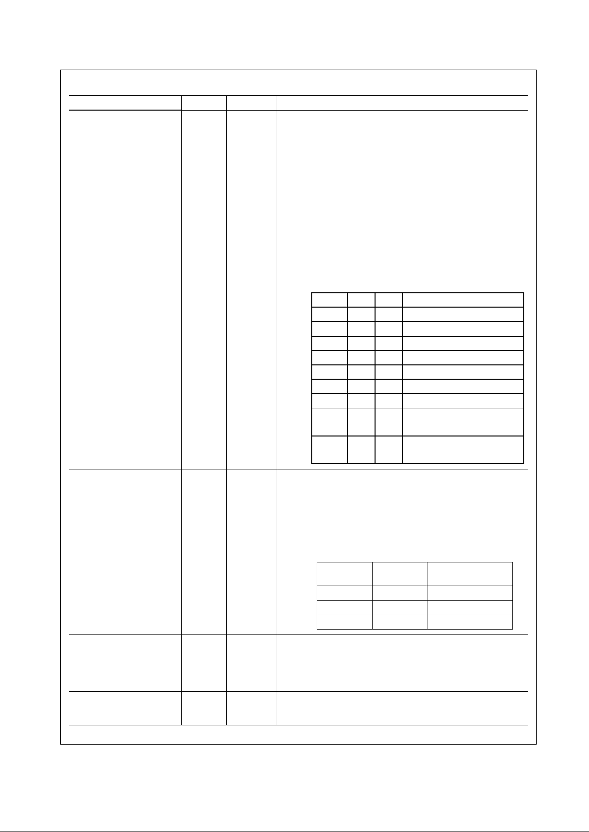
AN_EN AN1 AN0 Forced Mode
0 0 0 10BASE-T, Half-Duplex
0 0 1 10BASE-T, Full-Duplex
0 1 0 100BASE-TX, Half-Duplex
0 1 1 100BASE-TX, Full-Duplex
AN_EN AN1 AN0 Advertised Mode
1 0 0 10BASE-T, Half/Full-Duplex
1 0 1 100BASE-TX, Half/Full-Duplex
1 1 0 10BASE-T Half-Duplex
100BASE-TX, Half-Duplex
1 1 1 10BASE-T, Half/Full-Duplex
100BASE-TX, Half/Full-Duplex
MII_MODE SNI_MODE MAC Interface
Mode
0 X MII Mode
1 0 RMII Mode
1 1 10 Mb SNI Mode

14 www.national.com
DP83848C
1.7 10 Mb/s and 100 Mb/s PMD Interface
1.8 Special Connections
1.9 Power Supply Pins
Signal Name Type Pin # Description
TD-, TD+ I/O 16, 17 Differential common driver transmit output (PMD Output Pair).
These differential outputs are automatically configured to either
10BASE-T or 100BASE-TX signaling.
In Auto-MDIX mode of opera tion, this pair c an be used as the Receive Input pair.
These pins require 3.3V bias for operation.
RD-, RD+ I/O 13, 14 Differential receive input (PMD Input Pair). These differential in-
puts are automatically configured to accept either 100BASE-TX
or 10BASE-T signaling.
In Auto-MDIX mode of operation, this pair can be used as the
Transmit Output pair.
These pins require 3.3V bias for operation.
Signal Name Type Pin # Description
RBIAS I 24 Bias Resistor Connection. A 4.87 kΩ 1% resistor should be con-
nected from RBIAS to GND.
PFBOUT O 23 Power Feedback Output. Parallel caps, 10µ F (Tantalum pre-
ferred) and 0.1µF, should be placed close to the PFBOUT. Connect this pin to PFBIN1 (pin 18) and PFBIN2 (pin 37). See
Section 5.4 for proper placement pin.
PFBIN1
PFBIN2
I 18
37
Power Feedback Input. These pins are fed with power from
PFBOUT pin. A small capacitor of 0.1
µF should be connected
close to each pin.
Note: Do not supply power to these pins other than from
PFBOUT.
RESERVED I/O 8 , 9, 10, 11, 12RESERVED: These pins must be left unconnected.
RESERVED I/O 20, 21 RESERVED: These pins must be p ulled-u p throug h 2.2 k Ω resis-
tors to AVDD33 supply.
Signal Name Pin # Description
IOVDD33 32, 48 I/O 3.3V Supply
IOGND 35, 47 I/O Ground
DGND 36 Digital Ground
AVDD33 22 Analog 3.3V Supply
AGND 15, 19 Analog Ground

15 www.national.com
DP83848C
1.10 Package Pin Assignments
VBH48A Pin # Pin Name
1 TX_CLK
2 TX_EN
3 TXD_0
4 TXD_1
5 TXD_2
6 TXD_3/SNI_MODE
7 PWR_DOWN/INT
8 RESERVED
9 RESERVED
10 RESERVED
11 RESERVED
12 RESERVED
13 RD 14 RD +
15 AGND
16 TD 17 TD +
18 PFBIN1
19 AGND
20 RESERVED
21 RESERVED
22 AVDD33
23 PFBOUT
24 RBIAS
25 25MHz_OUT
26 LED_ACT/COL/AN_EN
27 LED_SPEED/AN1
28 LED_LINK/AN0
29 RESET_N
30 MDIO
31 MDC
32 IOVDD33
33 X2
34 X1
35 IOGND
36 DGND
37 PFBIN2
38 RX_CLK
39 RX_DV/MII_MODE
40 CRS/CRS_DV/LED_CFG
41 RX_ER/MDIX_EN
42 COL/PHYAD0
43 RXD_0/PHYAD1
44 RXD_1/PHYAD2
45 RXD_2/PHYAD3
46 RXD_3/PHYAD4
47 IOGND
48 IOVDD33
VBH48A Pin # Pin Name

16 www.national.com
DP83848C
2.0 Configuration
This section in clude s inform ation on the vari ous con figura tion options available with the DP83848C. The configuration options described below include:
— Auto-Negotiation
— PHY Address and LEDs
— Half Duplex vs. Full Duplex
— Isolate mode
— Loopback mode
—BIST
2.1 Auto-Negotiation
The Auto-Negotiation function provides a mechanism for
exchanging configuration information between two ends of
a link segment and automatically selecting the highest per
formance mode of operation supported by both devices.
Fast Link Pulse (FLP) Bursts provide the signalling used to
communicate Auto-Negotiation abilities between two
devices at each end of a link segment. For further detail
regarding Auto-Negotiation, refer to Clause 28 of the IEEE
802.3u specification. The DP83848C supports four differ
ent Ethernet protocols (10 Mb/s Half Duplex, 10 Mb/s Full
Duplex, 100 Mb/s Half Duplex, and 100 Mb/s Full Duplex),
so the inclusion of Auto-Negotiation ensures that the high
est performance protocol will be selected based on the
advertised ability of the Link Partner. The Auto-Negotiation
function within the DP83848C can be controlled either by
internal register access or by the use of the AN_EN, AN1
and AN0 pins.
2.1.1 Auto-Negotiation Pin Control
The state of AN_EN, AN0 an d AN1 det ermine s wheth er the
DP83848C is forced into a specific mode or Auto-Negotiation will advertise a specific ability (or set of abilities) as
given in
Tabl e 1. These pins allow configuration options to
be selected without requiring internal register access.
The state of AN_E N, AN0 and A N1, upon po wer-up/ reset,
determines the state of bits [8:5] of the ANAR register.
The Auto-Negotiation function selected at power-up or
reset can be chan ged at any time by writin g to the Basic
Mode Control Register (BMCR) at address 0x00h.
2.1.2 Auto-Negotiation Register Control
When Auto-Negotiation is enabled, the DP83848C transmits the abilities programmed into the Auto-Negotiation
Advertisement register (ANAR) at address 04h via FLP
Bursts. Any combination of 10 Mb/s, 100 Mb/s, HalfDuplex, and Full Duplex modes may be selected.
Auto-Negotiation Priority Resolution:
— (1) 100BASE-TX Full Duplex (Highest Priority)
— (2) 100BASE-TX Half Duplex
— (3) 10BASE-T Full Duplex
— (4) 10BASE-T Half Duplex (Lowest Priority)
The Basic Mode Control Register (BMCR) at address 00h
provides control for enabling, disabling, and restarting the
Auto-Negotiation process. When Auto-Negotiation is dis
abled, the Speed Selection bit in the BMCR controls
switching between 10 Mb/s or 100 Mb/s operation, and the
Duplex Mode bit controls switching between full duplex
operation and half duplex operation. The Speed Selection
and Duplex Mode bits have no effect on the mode of oper
ation when the Auto-Negotiation Enable bit is set.
The Link Speed can be examined through the PHY Status
Register (PHYSTS) at address 10h after a Link is
achieved.
The Basic Mode Status Register (BMSR) indicates the set
of available abilities for technology types, Auto-Negotiation
ability, and Extended Register Capability. These bits are
permanently set to indicate the full functionality of the
DP83848C (only the 100BASE-T4 bit is not set since the
DP83848C does not support that function).
The BMSR also provides status on:
— Whether or not Auto-Negotiation is complete
— Whether or not the Link Partner is advertising that a re-
mote fault has occurred
— Whether or not valid link has been established
— Support for Management Frame Preamble suppression
The Auto-Negotiation Advertisement Register (ANAR)
indicates the Auto-Negotiation abilities to be advertised by
the DP83848C. All available abilities are transmitted by
default, but any ability can be suppressed by writing to the
Table 1. Auto-Negotiation Modes
AN_EN AN1 AN0 Forced Mode
0 0 0 10BASE-T, Half-Duplex
0 0 1 10BASE-T, Full-Duplex
0 1 0 100BASE-TX, Half-Duplex
0 1 1 100BASE-TX, Full-Duplex
AN_EN AN1 AN0 Advertised Mode
1 0 0 10BASE-T, Half/Full-Duplex
1 0 1 100BASE-TX, Half/Full-Duplex
1 1 0 10BASE-T Half-Duplex
100BASE-TX, Half-Duplex
1 1 1 10BASE-T, Half/Full-Duplex
100BASE-TX, Half/Full-Duplex

17 www.national.com
DP83848C
ANAR. Updating the ANAR to suppress an ability is one
way for a management agent to change (restrict) the tech
-
nology that is used.
The Auto-Negotiation Link Partner Ability Register
(ANLPAR) at address 05h is used to receive the base link
code word as well as all next page code words during the
negotiati on. Furthermore, the ANLPAR will be updat ed to
either 0081h or 0021h for parallel detection to either 100
Mb/s or 10 Mb/s respectively.
The Auto-Negotiation Expansion Register (ANER) indicates additional Auto-Negotiation status. The ANER provides status on:
— Whether or not a Parallel Detect Fault has occurred
— Whether or not the Link Partne r supp orts the Next Pag e
function
— Whether or not the DP83848C supports the Next Page
function
— Whether or not the current page being exchanged by
Auto-Negotiation has been receiv ed
— Whether or not the Link Partner supports Auto-Negotia-
tion
2.1.3 Auto-Negotiation Parallel Detection
The DP83848C supports the Parallel Detection function as
defined in the IEEE 802.3u specifi ca tio n. Para lle l Detec tion
requires both the 10 Mb/s and 100 Mb/s receivers to moni
tor the receive signal and report link status to the AutoNegotiation function. Auto-Negotiation uses this informa
tion to configure th e correct t echno logy i n the e vent th at the
Link Partner does not support Auto-Negotiation but is
transmitting link signals that the 100BASE-TX or 10BASET PMAs recognize as valid link signa ls .
If the DP83848C completes Auto-Negotiation as a result of
Parallel Detection, bits 5 and 7 within the ANLPAR register
will be set to reflect the mode of operation present in the
Link Partner. Note that bits 4:0 of the ANLPAR will also be
set to 00001 based on a successful parallel detection to
indicate a valid 802.3 selector field. Software may deter
mine that negotiation completed via Parallel Detection by
reading a zero in the Link Partn er Au to-Neg oti ati on Ab le b it
once the Auto-Negotiatio n Com pl ete b it i s s et. I f co nfi gure d
for parallel detect mode and any condition other than a sin
gle good link occurs then the parallel detect fault bit will be
set.
2.1.4 Auto-Negotiation Restart
Once Auto-Negotiation has completed, it may be restarted
at any time by setting bit 9 (Res tart Auto-Negot iat ion) of the
BMCR to one. If the mode confi gured b y a su cces sful Aut oNegotiation loses a valid link, then the Auto-Negotiation
process will resume and attempt to determine the configu
ration for the link. This function ensures that a valid configuration is maintained if the cable becomes disconnected.
A renegotiation reques t fro m a ny en tity, such as a ma nag ement agent, will cause the DP83848C to halt any transmit
data and link pulse activity until the break_link_timer
expires (~1500 ms). Consequently, the Link Partner will go
into link fail and normal Auto-Negotiation resumes. The
DP83848C will resume Auto-Negotiation after the
break_link_timer has expired by issuing FLP (Fast Link
Pulse) bursts.
2.1.5 Enabling Auto-Negotiation via Software
It is important t o no te t hat if the DP83848C has been initialized upon power-up as a non-auto-negotiating device
(forced technology), and it is then requ ire d that Auto-Negotiation or re-Auto-Negotiation be initiated via software,
bit
12 (Auto-Negotiation Enable) of the Basic Mode Control
Register (BMCR) must first be cleared and then set for any
Auto-Negotiation function to take effect.
2.1.6 Auto-Negotiation Complete Time
Parallel detection and Auto-Negotiation take approximately
2-3 seconds to co mp let e. In addition, Auto-Negotiation with
next page should take approximately 2-3 seconds to com
-
plete, depending on the number of next pages sent.
Refer to Clause 28 of the IEEE 802.3u standard for a full
description of the individual timers related to Auto-Negotiation.
2.2 Auto-MDIX
When enabled, this function utilizes Auto-Negotiation to
determine the proper configuration for transmission and
reception of data and subsequently selects the appropriate
MDI pair for MD I/ MD IX o per a ti on. T h e fu nc t io n us es a r an
dom seed to control switching of the crossover circuitry.
This implementati on compl ie s with the corres po ndi ng IEEE
802.3 Auto-Negotiation and Crossover Specifications.
Auto-MDIX is enabled by default and can be configu r ed vi a
strap or via PHYCR (0x19h) register, bits [15:14].
Neither Auto-Negotiation nor Auto-MDIX is required to be
enabled in forcing crossover of the MDI pairs. Forced
crossover can be achieved through the FORCE_MDIX bit,
bit 14 of PHYCR (0x19h) register.
Note: Auto-MDIX will not work in a forced mode of operation.
18 www.national.com
DP83848C
2.3 PHY Address
The 5 PHY address inputs pins are shared with the
RXD[3:0] pins and COL pin as shown below.
The DP83848C can be set to res pond to any of 32 po ssibl e
PHY addresses via strap pins. The information is latched
into the PHYCR register (address 19h, bits [4:0]) at device
power-up and hardware reset. The PHY Address pins are
shared with the RXD and COL pins. Each DP83848C or
port sharing an MDIO bus in a system must have a unique
physical address.
The DP83848C supports PHY Address strapping values 0
( <000 00> ) th r ou gh 31 ( < 1 1111 > ) . St r a pp ing PHY Address
0 puts the part into Isol a t e Mod e. It should also be noted
that selecting PHY Address 0 via an MDIO write to PHYCR
will not put the device in Is olate Mode. Se e
Section 2.3.1for
more information.
For further detail relatin g to the la tch- in timi ng requi rement s
of the PHY Address pins, as well as the other hardware
configuration pins, refer to the Reset summary in
Section 6.0.
Since the PHYAD[0] pin has weak internal pull-up resistor
and PHYAD[4:1] pins have weak internal pull-down resis
tors, the default setting for the PHY address is 00001
(01h).
Refer to Figure 2 for an example o f a PHYAD connectio n to
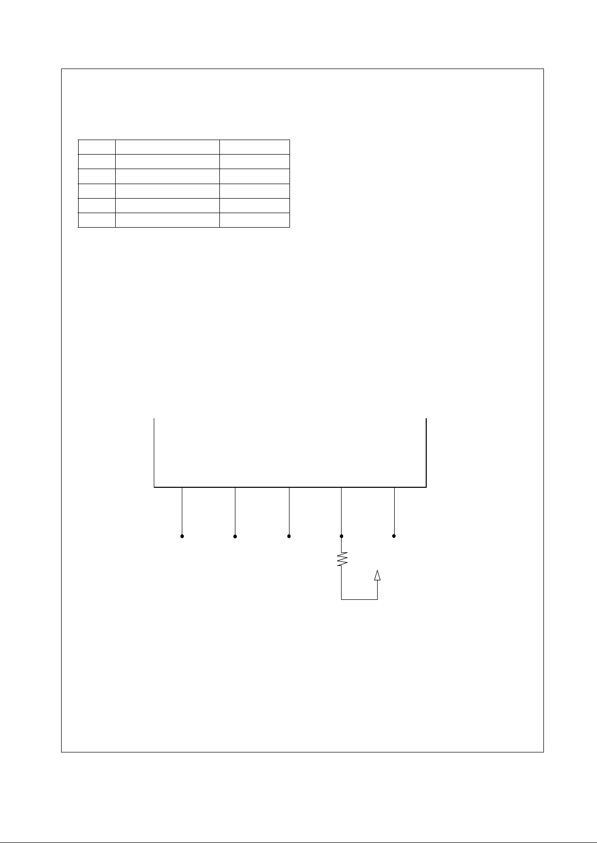
external c omponents. In this exam ple, the PHYAD strapping results in address 00011 (03h).
2.3.1 MII Isolate Mode
The DP83848C can be put into MII Isolate mode by writing
to bit 10 of t he BMCR regi ster or by st rapping in P hysical
Address 0. It should be noted that selecting Physical
Address 0 via an MDIO write to PHYCR will not put the
device in the MII isolate mode.
When in the MII isolate mode, the DP83848C does not
respond to packet data present at TXD[3:0], TX_EN inputs
and presents a high impedance on the TX_CLK, RX_CLK,
RX_DV, RX_ER, RXD[3:0], COL, and CRS outputs. When
in Isolate mode, the DP83848C will continue to respond to
all management transactions.
While in Isolate mod e, th e PM D ou tpu t p a ir wi ll n ot t r ansm it
packet data but will continue to source 100BASE-TX
scrambled idles or 10BASE-T normal link pulses.
The DP83848C can Auto-Negotiate or parallel detect to a
specific technology depending on the receive signal at the
PMD input pair. A valid link can be established for the
receiver even when the DP83848C is in Isolate mode.
Table 2. PHY Address Mapping
Pin # PHYAD Function RXD Function
42 PHYAD0 COL
43 PHYAD1 RXD_0
44 PHYAD2 RXD_1
45 PHYAD3 RXD_2
46 PHYAD4 RXD_3
Figure 2. PHYAD Strapping Example
COL
RXD_0
RXD_1
RXD_2
RXD_3
VCC
2.2kΩ
PHYAD0 = 1
PHYAD1 = 1
PHYAD2 = 0PHY AD3 = 0
PHYAD4= 0
19 www.national.com
DP83848C
2.4 LED Interface
The DP83848C supports three configurable Light Emitting
Diode (LED) pins. The device supports three LED configurations: Link, Speed, Activity and Collision. Function are
multiplexed among the LEDs. The PHY Control Register
(PHYCR) for the LEDs can also be selected through
address 19h, bits [6:5].
See Table 3 for LED Mode selection.
The LED_LINK pin in Mode 1 indicates the link status of
the port. In 100BASE-T mode, link is established as a
result of input receive amplitude compliant with the TPPMD specifications which will result in internal generation
of signal detect. A 10 Mb/s Link is est abli shed as a result of
the reception of at least seven consecutive normal Link
Pulses or the reception of a valid 10BASE-T packet. This
will cause the as se rtion of LED_LINK. LED_LINK will deas
sert in accordance with the Link Loss Timer as specified in
the IEEE 802.3 specification.
The LED_LINK p in in Mo de 1 w ill be OF F w h en no LI NK is
present.
The LED_LINK pin in Mode 2 and Mode 3 will be ON to
indicate Link is good and BLINK to indicate activity is
present on either transmit or receive activity.
The LED_SPEED pin indicates 10 or 100 Mb/s data rate of
the port. The standard CMOS driver goes high when operating in 100 Mb/s operation. The functionality of this LED is
independent of mode selected.
The LED_ACT/COL pin in Mode 1 indicates the presence
of either transmit or r ece iv e ac ti vit y. The LED will be ON for
Activity and OFF for No Activity. In Mode 2, this pin indi
cates the Collision status of the port. The LED will be ON
for Collision and OFF for No Collision.
The LED_ACT/COL pin in Mode 3 indicates the presence
of Duplex status for 10 Mb/s or 100 Mb/s operation. The
LED will be ON for Full Duplex and OFF for Half Duplex.
In 10 Mb/s half duplex mode, the collision LED is based on
the COL signal.
Since these LED pins are also used as strap options, the
polarity of the LED is dependent on whether the pin is
pulled up or down.
2.4.1 LEDs
Since the Auto-Negotiation (AN) strap options share the
LED output pins, the external components required for
strapping and LED usage must be considered in order to
avoid contention.
Specifically, when the LED outputs are used to drive LEDs
directly, the active state of each output driver is dependent
on the logic level sampled by the corresponding AN input
upon power-up/reset. For example, if a given AN input is
resistively pulled low then the corresponding output will be
configured as an active high driver. Conversely, if a given
AN input is resistively pulled high, then the corresponding
output will be configured as an active low driver.
Refer to Figure 3 for an example of AN connections to
external components. In this example, the AN strapping
results in Auto-Negotiation with 10/100 Half/Full-Duplex
advertised.
The adaptive nature of the LED outputs helps to simplify
potential implemen t ation issues o f th ese dual purpos e pins .
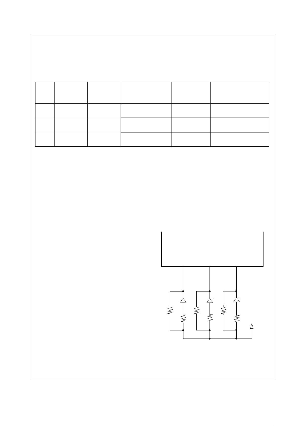
Table 3. LED Mode Select
Mode LED_CFG[1]
(bit 6)
LED_CFG[0]
(bit 5)
or (pin40)
LED_LINK LED_SPEED LED_ACT/COL
1 don’t care 1 ON for Good Link
OFF for No Link
ON in 100 Mb/s
OFF in 10 Mb/s
ON for Activity
OFF for No Activity
2 0 0 ON for Good Link
BLINK for Activity
ON in 100 Mb/s
OFF in 10 Mb/s
ON for Collision
OFF for No Collision
3 1 0 ON for Good Link
BLINK for Activity
ON in 100 Mb/s
OFF in 10 Mb/s
ON for Full Duplex
OFF for Half Duplex
LED_LINK
LED_SPEED
LED_ACT/COL
VCC
2.2kΩ
110Ω
110Ω
2.2kΩ
110Ω
AN0 = 1
AN1 = 1
AN_EN = 1
2.2kΩ
Figure 3. AN Strapping and LED Loading Example

20 www.national.com
DP83848C
2.4.2 LED Direct Control
The DP83848C provides another option to directly control
any or all LED outputs throu gh the LED Di rect Contro l Reg
ister (LEDCR), address 18h. The register does not provide
read access to LEDs.
2.5 Half Duplex vs. Full Duplex
The DP83848C supports both half and full duplex operation at both 10 Mb/s and 100 Mb/s speeds.
Half-duplex relies on the C SMA/C D protoc ol to ha ndle c ollisions and network access. In Half-Duplex mode, CRS
responds to both transmit and receive activity in order to
maintain compliance with the IEEE 802.3 specification.
Since the DP83848C is designed to support simultaneous
transmit and receiv e act ivi ty it is capabl e of su ppor ting full duplex switched ap plications with a throughput of up to 200
Mb/s per port when operating in 100BASE-TX mode.
Because the CSMA/CD protocol does not apply to fullduplex operation, the DP83848C disables its own internal
collision sensing and reporting functions and modifies the
behavior of Carrier Sense (CRS) such that it indicates only
receive acti vity. This allows a full-d uplex capable MAC to
operate properly.
All modes of operation (100BASE-TX and 10BASE-T) can
run either half-duplex or full-duplex. Additionally, other than
CRS and Collision reporting, all remaining MII signaling
remains the same regardless of the selected duplex mode.
It is important to understand that while Auto-Negotiation
with the use of Fast Link Pulse code words can interpret
and configure to full-duplex operation, parallel detection
can not recognize the difference between full and halfduplex from a fixed 10 Mb/s or 100 Mb/s link partner over
twisted pair. As specified in the 802.3u specification, if a
far-end link partner is configured to a forced full duplex
100BASE-TX ability, the parallel detection state machine in
the partner would be unable to detect the full duplex capa
bility of the far-end link partner. This link segment would
negotiate to a half duplex 100BASE-TX configuration
(same scenario for 10 Mb/s).
2.6 Internal Loopback
The DP83848C includes a Loopback Test mode for facilitating system diagnostics. The Loopback mode is selected
through bit 14 (Loopback) of the Basic Mode Control Reg
ister (BMCR). Writing 1 to this bit enables MII transmit data
to be routed to the MII receive outputs. Loopback status
may be checked in bit 3 of the PHY Status Register
(PHYSTS). While in Loopback mode the data will not be
transmitted onto the media. To ensure that the desired
operating mode is maintained, Auto-Negotiation should be
disabled before selecting the Loopback mode.
2.7 BIST
The DP83848C incorporates an internal Built-in Self Test
(BIST) circuit to accommodate in-circuit testing or diagnos
tics. The BIST circuit can be utilized to test the integrity of
the transmit and receive data paths. BIST testing can be
performed with the part in the internal loopback mode or
externally looped back using a loopback cable fixture.
The BIST is implemented with independent transmit and
receive paths, with the tran smit block generating a continu
ous stream of a pseudo random sequence. The user can
select a 9 bit or 15 bit pseudo random sequence from the
PSR_15 bit in the PHY Control Register (PHYCR). The
received data is compared to the generated pseudo-ran
dom data by the BIST Linear Feedback Shift Register
(LFSR) to determine the BIST pass/fail status.
The pass/fail status of the BIST is stored in the BIST status
bit in the PHYCR regis ter. The status bit de faul t s to 0 (BIST
fail) and will transition on a successful comparison. If an
error (mis-compare) occurs, the status bit is latched and is
cleared upon a subsequent write to the Start/Stop bit.
For transmit VOD testing, the Packet BIST Continuous
Mode can be used to allow continuous data transmission,
setting BIST_CONT_MODE, bit 5, of CDCTRL1 (0x1Bh).
The number of BIST errors can be monitored through the
BIST Error Count in the CDCTRL1 (0x1Bh), bits [15:8].

21 www.national.com
DP83848C
3.0 Functional Description
The DP83848C supports several modes of operation using
the MII interface pins. The optio ns are defi ned in th e follow
-
ing sections and include:
— MII Mode
— RMII Mode
— 10 Mb Serial Network Interface (SNI)
The modes of operation can be selected by strap options
or register control. For RMII mode, it is recommended to
use the strap option, since it requires a 50 MHz clock
instead of the normal 25 MHz.
In each of these modes, the IEEE 802.3 serial management interface is operational for device configuration and
status. The serial management interface of the MII allows
for the configuration and control of multiple PHY devices,
gathering of status, error information, and the determina
-
tion of the type and capabilities of the attached PHY(s).
3.1 MII Interface
The DP83848C incorporates the Media Independent Interface (MII) as specified in Clause 22 of the IEEE 802.3u
standard. This interface may be used to connect PHY
devices to a MAC in 10/100 Mb/s systems. This section
describes the nibble wide MII data interface.
The nibble wide MII data interface consists of a rec ei ve bus
and a transmit bus each with control signals to facilitate
data transfer between the PHY and the upper layer (MAC).
3.1.1 Nibble-wide MII Data Interface
Clause 22 of the IEEE 802.3u specification defines the
Media Independent Interface. This interface includes a
dedicated recei ve bu s an d a d edicated transmit bus. These
two data buses, along with various control and status sig
nals, allow for the simultaneous exchange of data between
the DP83848C and the upper layer agent (MAC).
The receive interface consists of a nibble wide data bus
RXD[3:0], a receive error signal RX_ER, a receive data
valid flag RX_DV, and a receive clock RX_CLK for syn
chronous transfer of the data. The receive clock operates
at either 2.5 MHz to su pport 10 Mb/s operation modes or at
25 MHz to support 100 Mb/s operational modes.
The transmit interface consists of a nibble wide data bus
TXD[3:0], a transmit enable control signal TX_EN, and a
transmit cloc k TX_CL K which runs at ei ther 2. 5 MHz or 25
MHz.
Additionally, the MII includes the carrier sense signal CRS,
as well as a collision detect signal COL. The CRS signal
asserts to ind icate the re ception of d ata from the ne twork
or as a function of transmit data in Half Duplex mode. The
COL signal asse rt s as an ind ic atio n of a collision which can
occur during half-duplex operation when both a transmit
and receive operation occur simultaneously.
3.1.2 Collision Detect
For Half Duplex, a 10BASE-T or 100BASE-TX collision is
detected when the receive and transmit channels are
active simu ltaneously. Collisions are reported by the COL
signal on the MII.
If the DP83848C is transmitting in 10 Mb/s mode when a
collision is dete cte d, the collision is not reported un til se ve n
bits have been received while in the collision state. This
prevents a collision being reported incorrectly due to noise
on the network. The COL signal remains set for the dura
-
tion of the collision.
If a collision occ urs du ring a r eceive operation, it is immedi-
ately reported by the COL signal.
When heartbeat is enabled (only applicable to 10 Mb/s
operation), approximately 1µs after the transmission of
each packet, a Si gn al Q u ali ty Error (SQE) signal of approx
imately 10 bit times is generated (internally) to indicate
successful transmiss io n. SQ E is repo rted as a pul se on th e
COL signal of the MII.
3.1.3 Carrier Sense
Carrier Sense (CRS) is asserted due to receive activity,
once valid data is detected via the squelch function during
10 Mb/s operation. During 100 Mb/s operation CRS is
asserted when a valid link (SD) and two non-contiguous
zeros are detected on the line.
For 10 or 100 Mb/s Half Duple x op era tio n, C RS is a sserte d
during either packet transmission or reception.
For 10 or 100 Mb/s Full Duplex operation, CRS is asserted
only due to receive activity.
CRS is deasserted following an end of packet.
3.2 Reduced MII Interface
The DP83848C incorporates the Reduced Media Independent Interface (RMII) as specified in the RMII specification
(rev1.2) from the RMII Consortium. This interface may be
used to connect PHY devices to a MAC in 10/100 Mb/s
systems using a reduced number of pins. In this mode,
data is transferred 2-bits at a time using the 50 MHz
RMII_REF clock for both transmit and receive. The follow
ing pins are used in RMII mode:
— TX_EN
—TXD[1:0]
— RX_ER (optional for Mac)
— CRS_DV
— RXD[1:0]
— X1 (RMII Reference clock is 50 MHz)
In addition, the RMII mode supplies an RX_DV signal
which allows for a simpler method of recovering receive
data without having to separate RX_DV from the CRS_DV
indication. This is especially useful for systems which do
not require CRS, such as systems that only support fullduplex operation. This signal is also useful for diagnostic
testing where it may be desirable to loop Receive RMII
data directly to the transmitte r.
Since the reference clock operates at 10 times the data
rate for 10 Mb/s operation, transmit data is sampled every
10 clocks. Likewise, receive data will be generated every
10th clock so that an attached device can sample the data
every 10 clocks.
RMII mode requires a 50 MHz oscillator be connected to
the device X1 pin. A 50 MHz crystal is not supported.

22 www.national.com
DP83848C
To tolerate potential frequency differences between the 50
MHz referenc e clock an d the recove red recei ve clock, the
receive RMII function includes a programmable elasticity
buffer. The elasticity buffer is programmable to minimize
propagation delay based on expected packet size and
clock accuracy. This allows for supporting a range of
packet sizes including jumbo frames.
The elasticity buffer will force Frame Check Sequence
errors for packets which overrun or underrun the FIFO.
Underrun and Overrun conditions can be reported in the
RMII and Bypass Register (RBR). The following table indi
cates how to program the elastic ity buff er fifo (in 4-bi t increments) based on expected max packet size and clock
accuracy. It assumes both clocks (RMII Reference clock
and far-end Transmitter clock) have the same accuracy.
3.3 10 Mb Serial Network Interface (SNI)
The DP83848C incorporates a 10 Mb Serial Network Interface (SNI) which al lo ws a s im pl e ser ial d ata interface for 10
Mb only devices. This is also referred to as a 7-wire inter
face. While there is no defined standard for this interface, it
is based on early 10 Mb physical layer devices. Data is
clocked serially at 10 MHz using separate transmit and
receive paths. The following pins are used in SNI mode:
—TX_CLK
—TX_EN
—TXD[0]
—RX_CLK
—RXD[0]
— CRS
—COL
3.4 802.3u MII Serial Management Interface
3.4.1 Serial Management Register Access
The serial management MII specification defines a set of
thirty-two 16-bit status and control registers that are acces
sible through the management interface pins MDC and
MDIO. The DP83848C implements all the required MII reg
isters as well as several optional registers. These registers
are fully described in
Section 7.0. A description of the seria l
management access protocol follows.
3.4.2 Serial Management Access Protocol
The serial cont rol interface co nsists of two pins, Management Data Clock (MDC) and Management Data Input/Output (MDIO). MDC has a maximum clock rate of 25 MHz
and no minimum rate. The MDIO line is bi-directional and
may be shared by up to 32 devices. The MDIO frame for
mat is shown below in Table 5.
The MDIO pin requires a pull-up resistor (1.5 kΩ) which,
during IDLE and turnaro und, will pull M DIO hi gh. In o rder to
initialize the MDIO int erface , the st atio n manag ement entit y
sends a sequence of 32 contiguous logic ones on MDIO to
provide the DP83848C with a sequence that can be used
to establish sy nchr oniz ati on. Th is pr eamb le may be gene r
ated either by driving MDIO high for 32 consecutive MDC
clock cycles, or by simply allowing the MDIO pull-up resis
tor to pull the MDIO pin high during which time 32 MDC
clock cycles are provided. In addition 32 MDC clock cycles
should be used to re-sync the device if an invalid start,
opcode, or turnaround bit is detected.
The DP83848C waits until it has received this preamble
sequence before responding to any other transaction.
Once the DP83848C serial management port has been ini
tialized no further preamble sequencing is required until
after a power-on/reset, invalid Start, invalid Opcode, or
invalid turnaround bit has occurred.
The St art co de is in dic ate d by a <01> p atte rn. Th is ass ure s
the MDIO line transitions from the default idle line state.
Turnaround is defined as an idle bit time inserted between
the Register Address field and the Data field. To avoid contention during a read transaction, no device shall actively
drive the MDIO signal during the first bit of Turnaround.
The addressed DP83848C drives the MDIO with a zero for
the second bit of turnaround and follows this with the
required data.
Figure 4 shows the timing relationship
between MDC and th e MDIO as dr iven/re ceived by the Station (STA) and the DP83848C (PHY) for a typical register
read access.
For write transactions, the station management entity
writes data to the addressed DP83848C thus eliminating
the requirement for MDIO Turnaround. The Turnaround
time is filled by the management entity by inserting <10>.
Figure 5 shows the timing relationship for a typical MII register write access.
Table 4. Supported packet sizes at +/-50ppm +/-100ppm for each clock
Start Threshold
RBR[1:0]
Latency Tolerance Recommende d Packet Size
at +/- 50ppm
Recommended Packet Size
at +/- 100ppm
1 (4-bits) 2 bits 24 00 byt es 1200 bytes
2 (8-bits) 6 bits 72 00 byt es 3600 bytes
3 (12-bits) 10 bits 12000 bytes 6000 bytes
0 (16-bits) 14 bits 16800 bytes 8400 bytes
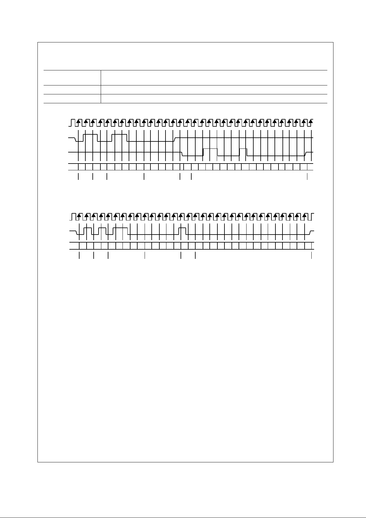
23 www.national.com
DP83848C
3.4.3 Serial Management Preamble Suppression
The DP83848C supports a Preamble Suppression mode
as indicated by a one in bit 6 of the Basic Mode Status
Register (BMSR, address 01h.) If the station management
entity (i.e. MAC or other management controller) deter
mines that all PHYs in the system support Preamble Suppression by returning a one in this bit, then the station
management entity need not generate preamble for each
management transaction.
The DP83848C requires a single initialization sequence of
32 bits of preamble fol lo w ing hard ware/s oftware reset. This
requirement is generally met by the mandatory pull-up
resistor on MDI O in co nj u nc tio n wi th a co nt i nuo u s MD C, or
the management access made to determine whether Pre
-
amble Suppression is supported.
While the DP83848C requires an initial preamble
sequence of 32 bits for management initialization, it does
not require a full 32-bit sequence between each subse
quent transaction. A minimum of one idle bit between man-
agement transactions is required as specified in the IEEE
802.3u specification.
Table 5. Typical MDIO Frame Format
MII Management
Serial Protocol
<idle><start><op code><device addr><reg addr><turnaround><data><idle>
Read Operation <idle><01><10><AAAAA><RRRRR><Z0><xxxx xxxx xxxx xxxx><idle>
Write Operation <idle><01><01><AAAAA><RRRRR><10><xxxx xxxx xxxx xxxx><idle>
Figure 4. Typical MDC/MDIO Read Operation
Figure 5. Typical MDC/MDIO Write Operation
MDC
MDIO
00011 110000000
(STA)
Idle Start
Opcode
(Read)
PHY Address
(PHYAD = 0Ch)
Register Address
(00h = BMCR)
TA
Register Data
Z
MDIO
(PHY)
Z
Z
Z
0 0 011000100000000
Z
Idle
Z
Z
MDC
MDIO
00011110000000
(STA)
Idle Start
Opcode
(Write)
PHY Address
(PHYAD = 0Ch)
Register Address
(00h = BMCR)
TA
Register Data
Z
0 0 0 000 00000000
Z
Idle
1000
ZZ
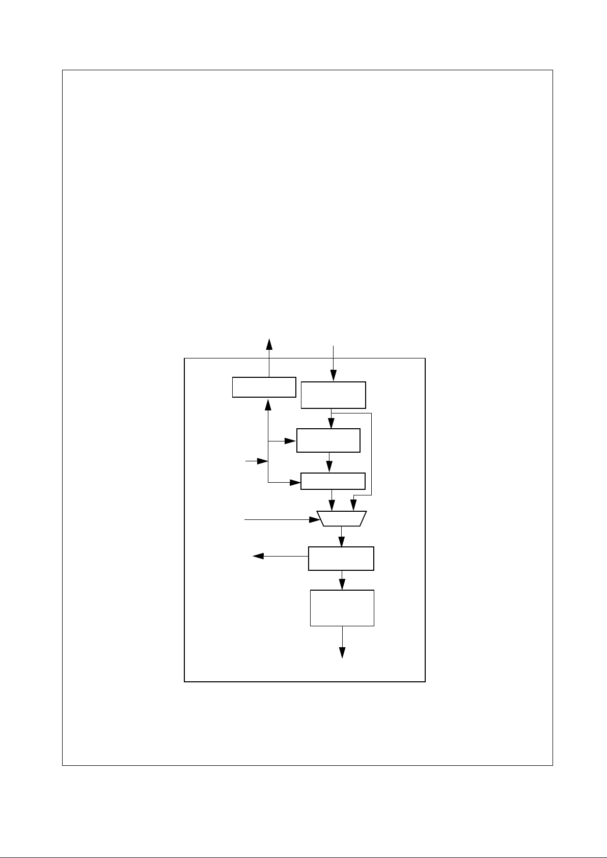
24 www.national.com
DP83848C
4.0 Architecture
This section describes the operations within each transceiver module, 100BASE-TX and 10BASE-T. Each operation consists of several functional blocks and described in
the following:
— 100BASE-TX Transmitter
— 100BASE-TX Receiver
— 10BASE-T Transceiver Module
4.1 100BASE-TX TRANSMITTER
The 100BASE-TX transmitter consists of several functional
blocks which conver t sync hronous 4-bit ni bble d at a, as p ro
vided by the MII, to a scrambled MLT-3 125 Mb/s serial
data stream. Because the 100BASE-TX TP-PMD is integrated, the differential output pins, PMD Output Pair, can
be directly routed to the magnetics.
The block diagram in Figure 6. provides an overview of
each functional block within the 100BASE-TX transmit section.
The Transmitter section consists of the following functional
blocks:
— Code-group Encoder and Injection block
— Scrambler block (bypass option)
— NRZ to NRZI encoder block
— Binary to MLT-3 converter / Common Driver
The bypass option for the functional blocks within the
100BASE-TX transmitter provides flexibility for applications
where data conversion is not always required. The
DP83848C implements the 100BASE-TX transmit state
machine diagram as specified in the IEEE 802.3u Stan
-
dard, Clause 24.
Figure 6. 100BASE-TX Transmit Block Diagram
4B5B CODE-
GROUP
ENCODER &
SCRAMBLER
NRZ TO NRZI
ENCODER
5B PARALLEL
TO SERIAL
PMD OUTPUT PAIR
TX_CLK
TXD[3:0] /
TX_EN
BINARY
TO MLT-3 /
COMMON
DRIVER
125MHZ CLOCK
BP_SCR
MUX
100BASE-TX
LOOPBACK
MLT[1:0]
DIVIDE
BY 5

25 www.national.com
DP83848C
Table 5. 4B5B Code-Group Encoding/Decoding
DATA CODES
0 11110 0000
1 01001 0001
2 10100 0010
3 10101 0011
4 01010 0100
5 01011 0101
6 01110 0110
7 01111 0111
8 10010 1000
9 10011 1001
A 10110 1010
B 10111 1011
C 11010 1100
D 11011 1101
E 11100 1110
F 11101 1111
IDLE AND CONTROL CODES
H 00100 HALT code-group - Error code
I 11111 Inter-Packet IDLE - 0000 (Note 1)
J 11000 First Start of Packet - 0101 (Note 1)
K 10001 Second Start of Packet - 0101 (Note 1)
T 01101 First End of Packet - 0000 (Note 1)
R 00111 Second End of Packet - 0000 (Note 1)
INVALID CODES
V 00000
V 00001
V 00010
V 00011
V 00101
V 00110
V 01000
V 01100
Note: Control code-groups I, J, K, T and R in data fields will be mapped as invalid codes, together with RX_ER asserted.
6.

26 www.national.com
DP83848C
4.1.1 Code-group Encoding and Injection
The code-group encoder converts 4-bit (4B) nibble data
generated by the MAC into 5-bit (5B) code-groups for
transmission. This conversion is required to allow control
data to be combined with packet data code-groups. Refer
to
Table 5 for 4B to 5B code-group mapping details.
The code-group encoder substitutes the first 8-bits of the
MAC preamble with a J/K code-group pair (11000 10001)
upon transmission. The code-group encoder continues to
replace subsequent 4B preamble and data nibbles with
corresponding 5B code-groups. At the end of the transmit
packet, upon the deassertion of Transmit Enable signal
from the MAC, the code-group encoder injects the T/R
code-group pair (01101 00111) indicating the end of the
frame.
After the T/R code-group pair, the code-group encoder
continuously injects IDLEs into the transmit data stream
until the next transmit packet is detected (reassertion of
Transmit Enable).
4.1.2 Scrambler
The scrambler is required to control the radiated emissions
at the media connector and on the twisted pair cable (for
100BASE-TX applications). By scrambling the data, the
total energy launched onto the cable is randomly distrib
uted over a wide frequency range. Without the scrambler,
energy levels at the PMD and on the cable could peak
beyond FCC limitations at frequencies related to repeating
5B sequences (i.e., continuous transmission of IDLEs).
The scrambler is configured as a closed loop linear feedback shift register (LFSR) with an 11-bit polynomial. The
output of the closed loop LFSR is X-ORd with the serial
NRZ data from the code-group encoder. The result is a
scrambled data stream with sufficient randomization to
decrease radiated emissions at certain frequencies by as
much as 20 dB. The DP83848C uses the PHY_ID (pins
PHYAD [4:0]) to set a unique seed value.
4.1.3 NRZ to NRZI Encoder
After the transmit data stream has been serialized and
scrambled, the data must be NRZI encoded in order to
comply with the TP-PMD standard for 100BASE-TX trans
mission over Category-5 Unshielded twisted pair cable.
4.1.4 Binary to MLT-3 Convertor
The Binary to MLT-3 conversion is accomplished by converting the serial binary data stream output from the NRZI
encoder into two binary data streams with alternately
phased logic one events. These two binary streams are
then fed to the twisted pa ir out put dri ve r whic h co nve r t s the
voltage to current and alternately drives either side of the
transmit transformer primary winding, resulting in a MLT-3
signal.
The 100BASE-TX MLT-3 signal sourced by the PMD Output Pair common driver is slew rate controlled. This should
be considered when selecting AC coupling magnetics to
ensure TP-PMD Standard compliant transition times (3 ns
< Tr < 5 ns).
The 100BASE-TX transmit TP-PMD function within the
DP83848C is capable of sourcing only MLT-3 encoded
data. Binary output from the PMD Output Pair is not possi
-
ble in 100 Mb/s mode.
4.2 100BASE-TX RECEIVER
The 100BASE-TX receiver consists of several functional
blocks which convert the scrambled MLT-3 125 Mb/s serial
data stream to synchronous 4-bit nibble data that is pro
vided to the MII. Because the 100BASE-TX TP-PMD is
integrated, the differential input pins, RD±, can be directly
routed from the AC coupling magnetics.
See Figure 7 for a block diagram of the 100BASE-TX
receive function. This provides an overview of each functional block within the 100BASE-TX receive section.
The Receive section consists of the following functional
blocks:
— Analog Front End
— Digital Signal Processor
— Signal Detect
— MLT-3 to Binary Decoder
— NRZI to NRZ Decoder
— Serial to Parallel
— Descrambler
— Code Group Alignment
—4B/5B Decoder
— Link Integrity Monitor
— Bad SSD Detection
4.2.1 Analog Front End
In addition to the Digital Equalization and Gain Control, the
DP83848C includes Analog Equalization and Gain Control
in the Analog Front End. The Analog Equalization reduces
the amount of Digital Equalization required in the DSP.
4.2.2 Digital Signal Processor
The Digital Signal Processor includes Adaptive Equalization with Gain Control and Base Line Wander Compensation.

27 www.national.com
DP83848C
4B/5B DECODER
DESCRAMBLER
MLT - 3 TO BINARY
DECODER
RX_CLK RXD[3:0] / RX_ER
NRZI TO NRZ
DECODER
CODE GROUP
ALIGNMENT
SERIAL TO
PARALLEL
RX_DV/CRS
RX_DATA
VALID SSD
DETECT
RD +/−
SIGNAL
DETECT
LINK
INTEGRITY
MONITOR
DIGITAL
SIGNAL
PROCESSOR
ANALOG
FRONT
END
Figure 7. 100BASE-TX Receive Block Diagram

28 www.national.com
DP83848C
4.2.2.1 Digital Adaptive Equalization and Gain Control
When transmitting data at high speeds over copper twisted
pair cable, frequency dependent attenuation becomes a
concern. In high-speed twisted pair signalling, the fre
quency content of the transmitted signal can vary greatly
during normal operation based primarily on the random
ness of the scrambled data stream. This variation in signal
attenuation caused by frequency variations must be com
pensated to ensure the integrity of the transmission.
In order to ensure quality transmission when employing
MLT-3 encod ing, the compen sation must be able to adapt
to various cable lengths and cable types depending on the
installed env ironment. The se lection of long cable lengths
for a given implementation, requires significant compensa
tion which will over-compensate for shorter, less attenuating lengths. Conversely, the selection of short or
intermediate cable lengths requiring less compensation will
cause serious under-compensation for longer length
cables. The compensation or equalization must be adap
-
tive to ensure proper conditioning of the received signal
independent of the cable length.
The DP83848C utilizes an extremely robust equalization
scheme referred as ‘Digital Adaptive Equalization.’
The Digital Equalizer removes ISI (inter symbol interference) from the receive data stream by continuously adapting to provide a filter with the inverse frequency response
of the channel. Equalization is combined with an adaptive
gain control stage. This enables the receive 'eye pattern' to
be opened sufficiently to allow very reliable data recovery.
The curves given in Figure 8 illustrate attenuation at certain
frequencies for given cable lengths. This is derived from
the worst case frequency vs. attenuation figures as speci
fied in the EIA/TIA Bulletin TSB-36. These curves indicate
the signific ant vari ations in signal at tenua tion that must be
compensated f or by the receive ad aptive equaliz ation cir
cuit.
Figure 8. EIA/TIA Attenuation vs. Frequency for 0 , 50,
100, 130 & 150 meters of CAT 5 cable

29 www.national.com
DP83848C
4.2.2.2 Base Line Wander Compensation
The DP83848C is comp letely ANSI TP -PMD comp li ant and
includes Base Line Wander (BLW) compensation. The
BLW compensation block can succ e ssf ul ly rec ov er th e T PPMD defined “killer” pattern.
BLW can generally be defined as the change in the average DC content, relatively short period over time, of an AC
coupled digital transmission over a given transmission
medium. (i.e., copper wire).
BLW results from the interaction between the low frequency components of a transmitted bit stream an d the frequency response of the AC coupling component(s) within
the transmission system. If the low frequency content of
the digital bit stream goes below the low frequency pole of
the AC coupling transformers then the droop characteris
tics of the transformers w ill do mi nate res ult ing in potentially
serious BLW.
The digital oscilloscope plot provided in Figure 9 illustrates
the severity of the BLW event that can theoretically be ge n erated during 100BASE-TX packet transmission. This
event consists of approximately 800 mV of DC offset for a
period of 120 µs. Left uncompensated, events such as this
can cause packet loss.
4.2.3 Signal Detect
The signal detect function of the DP838 48 C is incorpo rated
to meet the specificat ion s m an date d by the ANSI FD DI TP-
PMD Standard as well as the IEEE 802.3 100BASE-TX
Standard for both voltage thresholds and timing parame
-
ters.
Note that the reception of normal 10BASE-T link pulses
and fast link pulses per IEEE 802.3u Auto-Negotiation by
the 100BASE-TX receiver do not cause the DP83848C to
assert signal detect.
4.2.4 MLT-3 to NRZI Decoder
The DP83848C decodes the MLT-3 information from the
Digital Adaptive Equalizer block to binary NRZI data.
4.2.5 NRZI to NRZ
In a typical application, the NRZI to NRZ decoder is
required in order to present NRZ formatted data to the
descrambler.
4.2.6 Serial to Parallel
The 100BASE-TX receiver includes a Serial to Parallel
converter which supplies 5-bit wide data symbols to the
PCS Rx state machine.
Figure 9. 100BASE-TX BLW Event

30 www.national.com
DP83848C
4.2.7 Descrambler
A serial descrambler is used to de-scramble the received
NRZ data. The descrambler has to generate an identical
data scrambling sequence (N) in order to recover the origi
nal unscrambled data (UD) from the scrambled data (SD)
as represented in the equations:
Synchronization of the descrambler to the original scrambling sequence (N) is achieved based on the knowledge
that the incoming scrambled data stream consists of
scrambled IDLE data. After the descrambler has recog
nized 12 consecutive IDLE code-groups, where an
unscrambled I DLE code-group in 5B N RZ is equal to five
consecutive one s ( 11111), it will sync hronize to the receiv e
data stream and generate unscrambled data in the form of
unaligned 5B code-groups .
In order to maintain synchronization, the descrambler must
continuously monitor the validity of the unscrambled data
that it generates. To ensure this, a line state monitor and a
hold timer are used to constantly monitor the synchroniza
tion status. Upon synchronization of the descrambler the
hold timer star ts a 722 µs countdown. Upon detection of
sufficient IDLE code-groups (58 bit times) within the 722
µs
period, the hold timer will reset and begin a new count
down. This monitoring operation will continue indefinitely
given a properly operating network connection with good
signal integrity. If the line state monitor does not recognize
sufficient unscrambled ID LE code-gro ups within the 72 2
µs
period, the entire descrambler will be forced out of the cur
rent state of synchronization and reset in order to reacquire synchronization.
4.2.8 Code-group Alignment
The code-group alignment module operates on unaligned
5-bit data from the descrambler (or, if the descrambler is
bypassed, directly from the NRZI/NRZ decoder) and con
verts it into 5B code-group data (5 bits). Code-group alignment occurs after the J/K code-group pair is detected.
Once the J/K code-group pair (11000 10001) is detected,
subsequent data is aligned on a fixed boundary.
4.2.9 4B/5B Decoder
The code-group decoder functions as a look up table that
translates incoming 5B code-groups into 4B nibbles. The
code-group decoder first detects the J/K code-group pair
preceded by IDLE code-groups and replaces the J/K with
MAC preamble. Specifically, the J/K 10-bit code-group pair
is replaced by the nibble pair (0101 0101). All subsequent
5B code-groups are converted to the corresponding 4B
nibbles for the duration of the entire packet. This conver
sion ceases upon the detection of the T/R code-group pair
denoting the End of Stream Delimiter (ESD) or with the
reception of a minimum of two IDLE code-groups.
4.2.10 100BASE-TX Link Integrity Monitor
The 100 Base TX Lin k monito r ensur es that a v alid and st a ble link is established before enabling both the Transmit
and Receive PCS layer.
Signal detect must be vali d for 395u s to all ow the lin k monitor to enter the 'Lin k Up ' s tate, and enable the transmit and
receive functions.
4.2.11 Bad SSD Detection
A Bad Start of Stream Delimiter (Bad SSD) is any transition
from consecutive idle code-groups to non-idle code-groups
which is not prefixed by the code-group pair /J/K.
If this condition is detected, the DP83848C will assert
RX_ER and present RXD[3:0] = 1110 to the MII for the
cycles that correspond to received 5B code-groups until at
least two IDLE code groups are detected. In addition, the
False Carrier Sense Counter register (FCSCR) will be
incremented by one.
Once at least tw o IDLE co de groups are detec ted, RX_ER
and CRS become de-asserted.
4.3 10BASE-T TRANSCEIVER MODULE
The 10BASE-T Transceiver Module is IEEE 802.3 compliant. It includes the receiver, transmitter, collision, heartbeat, loopback, jabber, and link integrity functions, as
defined in the standard. An external filter is not required on
the 10BASE-T interface since this is integrated inside the
DP83848C. This section focuses on the genera l 10BASE-T
system level operation.
4.3.1 Operational Modes
The DP83848C has two basic 10BASE-T operational
modes:
— Half Du plex mode
— Full Duplex mode
Half Duplex Mode
In Half Duplex mode the DP83848C functions as a standard IEEE 802.3 10BASE-T transceiver supporting the
CSMA/CD protocol.
Full Duplex Mode
In Full Duplex mode the DP83848C is capable of simultaneously transmitting and receiving without asserting the
collision signal. The DP83848C's 10 Mb/s ENDEC is
designed to encode and decode simultaneously.
UD SD N⊕()=
SD UD N⊕()=

31 www.national.com
DP83848C
4.3.2 Smart Squelch
The smart squelch is responsible for determining when
valid data is present on the differential receive inputs. The
DP83848C implements an intelligent receive squelch to
ensure that impulse noise on the receive inputs will not be
mistaken for a valid signal. Smart squelch operation is
independent of the 10BASE-T operational mode.
The squelch circuitry employs a combination of amplitude
and timing measurements (as specified in the IEEE 802.3
10BSE-T standard) to determine the validity of data on the
twisted pair inputs (refer to
Figure 10).
The signal at the start of a packet is checked by the smart
squelch and any pulses not exceeding the squelch level
(either positive or negative, depending upon polarity) will
be rejected. Once this first squelch level is overcome cor
rectly, the opposite squelch level must then be exceeded
within 150 ns. Finally the signal must again exceed the
original squelch level within a 150 ns to ensure that the
input waveform will not be rejected. This checking proce
dure results in the loss of typically three preamble bits at
the beginning of each packet.
Only after all these conditions have been satisfied will a
control signal be generated to indicate to the remainder of
the circuitry that valid data is present. At this time, the
smart squelch circuitry is reset.
Valid data is considered to be present until the squelch
level has not been g enerated for a time longer than 150 ns,
indicating the End of Packet. Once good data has been
detected, the squelch levels are reduced to minimize the
effect of noise causing premature End of Packet detection.
4.3.3 Collision Detection and SQE
When in Half Duplex, a 10BASE-T collision is detected
when the receive and transmit channels are active simulta
neously. Collisions are reported by the COL signal on the
MII. Collisions are also reported when a jabber condition is
detected.
The COL signal remai ns set for the d uration of the c ollis ion.
If the PHY is receiving when a collision is detected it is
reported immediately (through the COL pin).
When heartbeat is enabled, approximately 1 µs after the
transmission of each packet, a Signal Quality Error (SQE)
signal of approximately 10-bit times is generated to indi
cate successful transmission. SQE is reported as a pulse
on the COL signal of the MII.
The SQE test is inhibited when the PHY is set in ful l du ple x
mode. SQE can also be inhibited by setting the
HEARTBEAT_DIS bit in the 10BTSCR register.
4.3.4 Carrier Sense
Carrier Sense (CRS) may be ass ert ed d ue to receive activity once valid data is detected via the squelch function.
For 10 Mb/s Half Duplex operation, CRS is asserted during
either packet transmission or reception.
For 10 Mb/s Full Duplex operation, CRS is asserted only
during receive activity.
CRS is deasserted following an end of packet.
4.3.5 Normal Link Pulse Detection/Generation
The link pulse generator produces pulses as defined in the
IEEE 802.3 10BASE-T standard. Each link pulse is nomi
nally 100 ns in duration and transmitted every 16 ms in the
absence of transmit data.
Link pulses are used to check the integrity of the connection with the remote end. If valid link pulses are not
received, the link detector disables the 10BASE-T twisted
pair transmitter, receiver and collision detection functions.
When the link integrity function is disabled
(FORCE_LINK_10 of the 10BTSCR register), a good link is
forced and the 10BASE-T transceiver will operate regard
less of the presence of link pulses.
end of packet
start of packet
V
SQ-(reduced)
V
SQ-
V
SQ+(reduced)
V
SQ+
<150 ns
<150 ns
>150 ns
Figure 10. 10BASE-T Twisted Pair Smart Squelch Operation

32 www.national.com
DP83848C
4.3.6 Jabber Function
The jabber function monitors the DP83848C's output and
disables the transmitte r if it att emp ts to transmit a packet of
longer than legal s iz e. A ja bbe r ti me r m oni tors th e transmit
ter and disables the transmission if the transmitter is active
for approximately 85 ms.
Once disabled by the Jabber function, the transmitter stays
disabled for the entire time that the ENDEC module's inter
nal transmit enable is asserted. This signal has to be deasserted for approximately 500 ms (the “unjab” time)
before the Jabber function re-enables the transmit outputs.
The Jabber function is only relevant in 10BASE-T mode.
4.3.7 Automatic Link Polarity Detection and Correction
The DP83848C's 10BASE-T transceiver module incorporates an automatic link polarity detection circuit. When
three consecutive inverted link pulses are received, bad
polarity is reported.
A polarity reversal can be cau sed by a wiring error a t eith er
end of the cable, usually at the Main Distribution Frame
(MDF) or patc h panel in the wiring closet.
The bad polarity conditi on is la tched in th e 10BTS CR register. The DP83848C's 10BASE-T transceiver module corrects for this error internally and will continue to decode
received data correctly. This eliminates the need to correct
the wiring error immediately.
4.3.8 Transmit and Receive Filtering
External 10BASE-T filters are not required when using the
DP83848C, as the required signal conditioning is inte
-
grated into the device.
Only isolation transformers and impedance matching resis-
tors are required for the 10BASE-T transmit and receive
interface. The internal transmit filtering ensures that all the
harmonics in the transmit signal are attenuated by at least
30 dB.
4.3.9 Transmitter
The encoder begins operation when the Transmit Enable
input (TX_EN) goes high and converts NRZ data to preemphasized Manchester data for the transceiver. For the
duration of TX_EN, the serialized Transmit Data (TXD) is
encoded for the transmit-driver pair (PMD Output Pair).
TXD must be valid on the rising edge of Transmit Clock
(TX_CLK). Transmission ends when TX_EN deasserts.
The last transition is always positive; it occurs at the center
of the bit cell if the last bit is a one, or at the end of the bit
cell if the last bit is a zero.
4.3.10 Receiver
The decoder detects the en d of a frame when no additional
mid-bit transitions are detected. Within one and a half bit
times after the last bit, carrier sense is de-asserted.
Receive clock st ays active for five more bit times after CRS
goes low, to guarantee the receive timings of the controller.

33 www.national.com
DP83848C
5.0 Design Guidelines
5.1 TPI Network Circuit
Figure 11 shows the recommended circuit for a 10/100
Mb/s twisted pair interface. To the right is a partial list of
recommended transformers. It is important that the user
realize that variations with PCB and component character
istics requires that the application be tested to ensure that
the circuit meets the requirements of the intended application.
Pulse H1102
Pulse H2019
Pulse J0011D21
Pulse J0011D21B
Figure 11. 10/100 Mb/s Twisted Pair Interface
RJ45
RD-
RD+
TD-
TD+
RDRD+
TDTD+
1:1
0.1µF*
T1
1:1
COMMON MODE CHOKES
MAY BE REQUIRED.
49.9Ω
49.9
Ω
0.1µF*
Vdd
NOTE: CENTER TAP IS PULLED TO VDD
*PLACE CAPACITORS CLOSE TO THE
TRANSFORMER CENTER TAPS
0.1µF
All values are typical and are +/- 1%
PLACE RESISTORS AND
CAPACITORS CLOSE TO
THE DEVICE.
Vdd
49.9Ω
49.9
Ω
0.1µF
Vdd

34 www.national.com
DP83848C
5.2 ESD Protection
Typically, ESD precautions are predominantly in effect
when handling the devices or board before being installed
in a system. In those cases, strict handling procedures
need be implemented during the manufacturing process to
greatly reduce the occurrences of catastrophic ESD
events. After the system is assembled, internal compo
-
nents are less sensitive from ESD events.
See Section 8.0 for ESD rating.
5.3 Clock In (X1) Requirements
The DP83848C support s an ex tern al C MOS lev el os cil la tor
source or a crystal resonator device.
Oscillator
If an external clock sour ce i s us ed, X1 sho uld be ti ed to the
clock source and X2 should be left floating.
Specifications for CMOS oscillators: 25 MHz in MII Mode
and 50 MHz in R MII M ode are listed in
Table 6 and Table 8.
Note: Maximum Reference Clock Jitter should not exceed
1ns peak-to-peak or 78ps rms from 50 kHz to 1 MHz.
Crystal
A 25 MHz, parallel, 20 pF load crystal resonator should be
used if a crystal source is desired.
Figure 12 shows a typi-
cal connection for a crystal resonator circuit. The load
capacitor values will vary with the crystal vendors; check
with the vendor for the recommended loads.
The oscillator circuit is designed to drive a parallel resonance AT cut crystal with a minimum drive level of 100µW
and a maximum of 500µW. If a crystal is specified for a
lower drive level, a current limiting resistor should be
placed in series between X2 and the crystal.
As a starting p oint fo r evalu ating an o scillat or circ uit, if t he
requirements for the crystal are not known, C
L1
and C
L2
should be set at 33 pF, and R1 should be set at 0Ω.
Specification for 25 MHz crystal are listed in Table 9.
Figure 12. Crystal Oscillator Circuit
X1
X2
C
L2
C
L1
R
1
Table 6. 25
Table 7. 25 MHz Oscillator Specification
Parameter Min Typ Max Units Condition
Frequency 25 MHz
Frequency
Tolerance
+50 ppm Operational Temperature
Frequency
Stability
+50 ppm 1 year aging
Rise / Fall Time 6 nsec 20% - 80%
Jitter (Short term) 50 psec Cycle-to-cycle
Jitter (Long term) 1 nsec Accumulative over 10us
Symmetry 40% 60% Duty Cycle
Table 8. 50 MHz Oscillator Specification
Parameter Min Typ Max Units Condition
Frequency 50 MHz
Frequency
Tolerance
+50 ppm Operational
Temperature
Frequency
Stability
+50 ppm Operational
Temperature
Rise / Fall Time 6 nsec 20% - 80%
Jitter (Short term) 50 psec Cycle-to-cycle
Jitter (Long term) 1 nsec Accumulative over 10us
Symmetry 40% 60% Duty Cycle

35 www.national.com
DP83848C
5.4 Power Feedback Circuit
To ensure correct operation for the DP83848C, parallel
caps with values of 10 µF (Tantalum) and 0.1 µF shou ld be
placed close to pin 23 (PFBOUT) of the device.
Pin 18 (PFBIN1) and pin 37 (PFBIN2) must be connected
to pin 23 (PFBOUT), each pin requires a smal l capacitor
(.1
µF). See Figure 13 below for proper connections.
5.5 Power Down/Interrupt
The Power Down and Interrupt functions are multiplexed
on pin 7 of the device. By default, this pin functions as a
power down input and the interrupt function is disabled.
Setting bit 0 (INT_OE) of MICR (0x11h) will configure the
pin as an active low interrupt output.
5.5.1 Power Down Control M ode
The PWR_DOWN /INT pin can b e asserted low t o put the
device in a Power Down m od e. Th is i s eq uiv al ent t o se ttin g
bit 11 (Power Down) in the Basic Mode Control Register,
BMCR (0x00h). An external control signal can be used to
drive the pin low, overcoming the weak internal pull-up
resistor. Alternatively, the device can be configured to ini
-
tialize into a Power Down state by use of an external pull-
down resistor on the PWR_DOWN/INT pin. Since the
device will still respond to management register accesses,
setting the INT_OE bit in the MICR register will disable the
PWR_DOWN/INT input, allowing the device to exit the
Power Down state.
5.5.2 Interrupt Mechanisms
The interrupt function is controlled via register access. All
interrupt sources are disabled by default. Setting bit 1
(INTEN) of MICR (0x11h) will enable interrupts to be out
put, dependent on the interrupt mask set in the lower byte
of the MISR (0x12h). The PWR_DOWN/INT pin is asyn
chronously asserted low when an interrupt condition
occurs. The source of the interrupt can be determined by
reading the upper byte of the MIS R. One or more bit s in th e
MISR will be set, denoting all currently pending interrupts.
Reading of the MISR clears ALL pending interrupts.
Example: To generate an interrupt on a change of link status or on a change of energy detect power state, the steps
would be:
— Write 0003h to MICR to set INTEN and INT_OE
— Write 0060h to MISR to set ED_INT_EN and
LINK_INT_EN
— Monitor PWR_DOWN/INT pin
When PWR_DOWN/INT pin asserts low, user would read
the MISR register to see if the ED_INT or LINK_INT bits
are set, i.e. which source caused the interrupt. After read
ing the MISR, the interrupt bits should clear and the
PWR_DOWN/INT pin will deassert.
5.6 Energy Detect Mode
When Energy Detect is enabled and there is no activity on
the cable, the DP83848C will remain in a low power mode
while monitoring the transmission line. Activity on the line
will cause the DP83848C to go through a normal power up
sequence. Regardless of cable activity, the DP83848C will
occasionally wake up the transmitter to put ED pulses on
the line, but will otherwise draw as little power as possible.
Energy detect functionality is controlled via register Energy
Detect Control (EDCR), address 0x1Dh.
Table 9. 25 MHz Crys tal Specification
Parameter Min Typ Max Units Condition
Frequency 25 MHz
Frequency
Tolerance
+50 ppm Operational Tem-
perature
Frequency
Stability
+50 ppm 1 year aging
Load Capacitance 25 40 pF
.1 µ
F
10 µF
Pin 23 (
PFBOUT
)
.1 µF
.1 µF
Pin 18 (PFBIN1)
Pin 37 (PFBIN2)
+
-
Figure 13. Power Feeback Connection

36 www.national.com
DP83848C
6.0 Reset Operatio n
The DP83848C includes an internal power-on reset (POR)
function and does not need to be explicitly reset for normal
operation after power up. If required during normal opera
tion, the device can be reset by a hardware or software
reset.
6.1 Hardware Reset
A hardware reset is accomplished by applying a low pulse
(TTL level), with a duration of at least 1
µs, to the
RESET_N. This will reset the device such that all registers
will be reinitialized to default values and the hardware con
-
figuration values will be re-latched into the device (similar
to the power-up/reset operation).
6.2 Software Reset
A software reset is accomplished by setting the reset bit
(bit 15) of the Basic Mode Control Register (BMCR). The
period from the point in time when the reset bit is set to the
point in time when software reset has concluded is approx
-
imately 1 µs.
The software reset will reset the device such that all regis-
ters will be reset to defau lt v alu es and the h ardwa re configuration values will be maintained. Software driver code
must wait 3
µs following a software reset before allowing
further serial MII operations with the DP83848C.

37 www.national.com
DP83848C
7.0 Register Block
Table 10. Register Map
Offset
Access Tag Description
Hex Decimal
00h 0 RW BMCR Basic Mode Control Register
01h 1 RO BMSR Basic Mode Status Register
02h 2 RO PHYIDR1 PHY Identifier Register #1
03h 3 RO PHYIDR2 PHY Identifier Register #2
04h 4 RW ANAR Auto-Negotiation Advertisement Register
05h 5 RW ANLPAR Auto-Negotiation Link Partner Ability Register (Base Page)
05h 5 RW ANLPARNP Auto-Negotiation Link Partner Ability Register (Next Page)
06h 6 RW ANER Auto-Negotiation Expansion Register
07h 7 RW ANNPTR Auto-Negotiation Next Page TX
08h-Fh 8-15 RW RESERVED RESERVED
Extended Registers
10h 16 RO PHYSTS PHY Status Register
11h 17 RW MICR MII Interrupt Control Register
12h 18 RO MISR MII Interrupt Status Register
13h 19 RW RESERVED RESERVED
14h 20 RO FCSCR False Carrier Sense Counter Register
15h 21 RO RECR Receive Error Counter Register
16h 22 RW PCSR PCS Sub-Layer Configuration and Status Register
17h 23 RW RBR RMII and Bypass Register
18h 24 RW LEDCR LED Direct Control Register
19h 25 RW PHYCR PHY Control Register
1Ah 26 RW 10BTSCR 10Base-T Status/Control Register
1Bh 27 RW CDCTRL1 CD Test Control Register and BIST Extensions Register
1Ch 28 RW RESERVED RESERVED
1Dh 29 RW EDCR Energy Detect Control Register
1Eh-1Fh 30-31 RW RESERVED RESERVED

38 www.national.com
Table 11. Register Table
Register Name Addr Tag Bit 15 Bit 14 Bit 13 Bit 12 Bit 11 Bit 10 Bit 9 Bit 8 Bit 7 Bit 6 Bit 5 Bit 4 Bit 3 Bit 2 Bit 1 Bit 0
Basic Mode Control Register
00h BMCR Reset Loop-
back
Speed
Selection
Auto-
Neg
Enable
Power
Down
Isolate Restart
Auto-
Neg
Duplex
Mode
Collision
Test
Re-
served
Re-
served
Re-
served
Re-
served
Re-
served
Re-
served
Re-
served
Basic Mode Status Register
01h BMSR 100Base
-T4
100Base
-TX FDX
100Base
-TX HDX
10Base-
T
FDX
10Base-
T
HDX
Re-
served
Re-
served
Re-
served
Re-
served
MF Pre-
amble
Sup-
press
Auto-
Neg
Com-
plete
Remote
Fault
Auto-
Neg
Ability
Link
Status
Jabber
Detect
Extend-
ed Capa-
bility
PHY Identifier Register 1
02h PHYIDR
1
OUI MSB OUI MSB OUI MSB OUI MSB OUI MSB OUI MSB OUI MSB OUI MSB OUI MSB OUI MSB OUI MSB OUI MSB OUI MSB OUI MSB OUI MSB OUI MSB
PHY Identifier Register 2
03h PHYIDR
2
OUI LSB OUI LSB OUI LSB OUI LSB OUI LSB OUI LSB VNDR_
MDL
VNDR_
MDL
VNDR_
MDL
VNDR_
MDL
VNDR_
MDL
VNDR_
MDL
MDL_
REV
MDL_
REV
MDL_
REV
MDL_
REV
Auto-Negotiation Advertisement Register
04h ANAR Next
Page Ind
Re-
served
Remote
Fault
Re-
served
ASM_DI
R
PAUSE T4 TX_FD TX 10_FD 10 Protocol
Selection
Protocol
Selection
Protocol
Selection
Protocol
Selection
Protocol
Selection
Auto-Negotiation Link Partner Ability Regis-
ter (Base Page)
05h ANLPAR Next
Page Ind
ACK Remote
Fault
Re-
served
ASM_DI
R
PAUSE T4 TX_FD TX 10_FD 10 Protocol
Selection
Protocol
Selection
Protocol
Selection
Protocol
Selection
Protocol
Selection
Auto-Negotiation Link Partner Ability Regis-
ter Next Page
05h AN-
LPARNP
Next
Page Ind
ACK Mes-
sage
Page
ACK2 Toggle Code Code Code Code Code Code Code Code Code Code Code
Auto-Negotiation Expansion Register
06h ANER Re-
served
Re-
served
Re-
served
Re-
served
Re-
served
Re-
served
Re-
served
Re-
served
Re-
served
Re-
served
Re-
served
PDF LP_NP_
ABLE
NP_
ABLE
PAGE_
RX
LP_AN_
ABLE
Auto-Negotiation Next Page TX Register
07h ANNPTR Next
Page Ind
Re-
served
Mes-
sage
Page
ACK2 TOG_TX CODE CODE CODE CODE CODE CODE CODE CODE CODE CODE CODE
RESERVED
08-0fh Re-
served
Re-
served
Re-
served
Re-
served
Re-
served
Re-
served
Re-
served
Re-
served
Re-
served
Re-
served
Re-
served
Re-
served
Re-
served
Re-
served
Re-
served
Re-
served
Re-
served
EXTENDED REGISTERS
PHY Status Register
10h PHYSTS Re-
served
MDI-X
mode
Rx Err
Latch
Polarity
Status
False
Carrier
Sense
Signal
Detect
De-
scram
Lock
Page
Receive
MII Inter-
rupt
Remote
Fault
Jabber
Detect
Auto-
Neg
Com-
plete
Loop-
back Sta-
tus
Duplex
Status
Speed
Status
Link
Status
MII Interrupt Control Register
11h MICR Re-
served
Re-
served
Re-
served
Re-
served
Re-
served
Re-
served
Re-
served
Re-
served
Re-
served
Re-
served
Re-
served
Re-
served
Re-
served
TINT INTEN INT_OE
MII Interrupt Status and Misc. Control Reg-
ister
12h MISR Re-
served
ED_INT LINK_IN
T
SPD_IN
T
DUP_IN
T
ANC_IN
T
FHF_INT RHF_IN
T
Re-
served
UNMSK_
ED
UNMSK_
LINK
UNMSK_
JAB
UNMSK_
RF
UNMSK_
ANC
UNMSK_
FHF
UNMSK_
RHF
RESERVED
13h Re-
served
Re-
served
Re-
served
Re-
served
Re-
served
Re-
served
Re-
served
Re-
served
Re-
served
Re-
served
Re-
served
Re-
served
Re-
served
Re-
served
Re-
served
Re-
served
Re-
served
False Carrier Sense Counter Register
14h FCSCR Re-
served
Re-
served
Re-
served
Re-
served
Re-
served
Re-
served
Re-
served
Re-
served
FCSCNT FCSCNT FCSCNT FCSCNT FCSCNT FCSCNT FCSCNT FCSCNT
Receive Error Counter Register
15h RECR Re-
served
Re-
served
Re-
served
Re-
served
Re-
served
Re-
served
Re-
served
Re-
served
RXER-
CNT
RXER-
CNT
RXER-
CNT
RXER-
CNT
RXER-
CNT
RXER-
CNT
RXER-
CNT
RXER-
CNT
PCS Sub-Layer Configuration and Status
Register
16h PCSR Re-
served
Re-
served
Re-
served
BYP_4B
5B
Re-
served
TQ_EN SD_FOR
CE_PMA
SD_
OPTION
DESC_T
IME
Re-
served
FORCE_
100_OK
Re-
served
Re-
served
NRZI_
BYPASS
SCRAM_
BYPASS
DE
SCRAM_
BYPASS

39 www.national.com
RMII and Bypass Register
17h RBR Re-
served
Re-
served
Re-
served
Re-
served
Re-
served
Re-
served
Re-
served
Re-
served
Re-
served
Re-
served
RMII_M
ODE
RMII_RE
V1_0
RX_OVF
_STS
RX_UNF
_STS
RX_RD_
PTR[1]
RX_RD_
PTR[0]
LED Direct Control Register
18h LEDCR Re-
served
Re-
served
Re-
served
Re-
served
Re-
served
Re-
served
Re-
served
Re-
served
Re-
served
Re-
served
DRV_SP
DLED
DRV_LN
KLED
DRV_AC
TLED
SPDLED LNKLED ACTLED
PHY Control Register
19h PHYCR MDIX_E
N
FORCE_
MDIX
PAUSE_
RX
PAUSE_
TX
BIST_fe PSR_15 BIST_
STATUS
BIST_ST
ART
BP_STR
ETCH
LED_
CNFG[1]
LED_
CNFG[0]
PHY
ADDR
PHY
ADDR
PHY
ADDR
PHY
ADDR
PHY
ADDR
10Base-T Status/Control Register
1Ah 10BT_S
ERIAL
10BT_S
ERIAL
REJECT
100
BASE T
ERROR
RANGE
ERROR
RANGE
SQUELC
H
SQUELC
H
SQUELC
H
LOOPBA
CK_10_
DIS
LP_DIS FORC_
LINK_10
Re-
served
POLARI-
TY
Re-
served
Re-
served
HEART_
DIS
JABBER
_DIS
CD Test Control and BIST Extensions Reg-
ister
1Bh CDCTRL
1
BIST_ER
ROR_C
OUNT
BIST_ER
ROR_C
OUNT
BIST_ER
ROR_C
OUNT
BIST_ER
ROR_C
OUNT
BIST_ER
ROR_C
OUNT
BIST_ER
ROR_C
OUNT
BIST_ER
ROR_C
OUNT
BIST_ER
ROR_C
OUNT
Re-
served
Re-
served
BIST_C
ONT_M
ODE
CDPattE
N_10
Re-
served
10Meg_
Patt_Ga
p
CDPatt-
Sel
CDPatt-
Sel
RESERVED
1Ch Re-
served
Re-
served
Re-
served
Re-
served
Re-
served
Re-
served
Re-
served
Re-
served
Re-
served
Re-
served
Re-
served
Re-
served
Re-
served
Re-
served
Re-
served
Re-
served
Re-
served
Energy Detect Control Register
1Dh EDCR ED_EN ED_AUT
O_UP
ED_AUT
O_DOW
N
ED_MAN ED_BUR
ST_DIS
ED_PW
R_STAT
E
ED_ERR
_MET
ED_DAT
A_MET
ED_ERR
_COUNT
ED_ERR
_COUNT
ED_ERR
_COUNT
ED_ERR
_COUNT
ED_DAT
A_COUN
T
ED_DAT
A_COUN
T
ED_DAT
A_COUN
T
ED_DAT
A_COUN
T
RESERVED
1Eh-1Fh Re-
served
Re-
served
Re-
served
Re-
served
Re-
served
Re-
served
Re-
served
Re-
served
Re-
served
Re-
served
Re-
served
Re-
served
Re-
served
Re-
served
Re-
served
Re-
served
Re-
served
Table 11. Register Table
Register Name Addr Tag Bit 15 Bit 14 Bit 13 Bit 12 Bit 11 Bit 10 Bit 9 Bit 8 Bit 7 Bit 6 Bit 5 Bit 4 Bit 3 Bit 2 Bit 1 Bit 0

40 www.national.com
DP83848C
7.1 Register Definition
In the register definitions under the ‘Default’ heading, the following definitions hold true:
— RW=Read Write access
— SC=Register sets on event occurrence and Self-Clears when event ends
— RW/SC =Read Write access/Self Clearing bit
— RO=Read Only access
— COR = Clear on Read
— RO/COR=Read Only, Clear on Read
— RO/P=Read Only, Permanently set to a default value
— LL=Latched Low and held until read, based upon the occurrence of the corresponding event
—LH=Latched High and held until read, based upon the occurrence of the corresponding event

41 www.national.com
DP83848C
7.1.1 Basic Mode Control Register (BMCR)
Table 12. Basic Mode Control Register (BMCR), address 0x00
Bit Bit Name Default Description
15 Reset 0, RW/SC Reset:
1 = Initiate software Reset / Reset in Process.
0 = Normal operation.
This bit, which is self-clearing, returns a value of one until the reset
process is complete. The configuration is re-strapped.
14 Loopback 0, RW Loopback:
1 = Loopback enabled.
0 = Normal operation.
The loopback functio n enables MII transmit dat a to be routed to the MII
receive data path.
Setting this bit may cause the descram bler to lose synchroni zation and
produce a 500 µs “dead ti me ” befo re any valid data will appear at the
MII receive outputs.
13 Speed Selection Strap, RW Speed Select:
When auto-negotiation is disabled writing to this bit allows the port
speed to be selected.
1 = 100 Mb/s.
0 = 10 Mb/s.
12 Auto-Negotiation
Enable
Strap, RW Auto-Negotiation Enable:
Strap controls initial value at reset.
1 = Auto-Negotiation Enabled - bits 8 and 13 of this register are ig-
nored when this bit is set.
0 = Auto-Negotiati on Disabled - bits 8 and 13 determine t he port speed
and duplex mode.
11 Power Down 0, RW Power Down:
1 = Power down.
0 = Normal operation.
Setting this bit powers down the PHY. Only the register block is en-
abled during a power down condition. This bit is OR’d with the input
from the PWR_DOWN/INT pin. When the active low
PWR_DOWN/INT pin is asserted, this bit will be set.
10 Isolate 0, RW Isolate:
1 = Isolates the Port fro m t he M II wi th the exception of the serial management.
0 = Normal operation.
9 Restart Auto-
Negotiation
0, RW/SC Restart Auto-Negotiation:
1 = Restart Auto-Negotiation. Re-initiates the Auto-Negotiation process. If Auto-Negotiati on is disabled (bit 12 = 0), this bit is ig nored. This
bit is self-clearing and w ill retu rn a val ue of 1 u nti l Au to-N eg oti ati on i s
initiated, whereupo n it will self-clear. Opera tion of the Auto-Negotiati on
process is not affected by the management entity clearing this bit.
0 = Normal operation.
8 Duplex Mode Strap, RW Duplex Mode:
When auto-negotiatio n is disabled wri ting to this bit allows the port Duplex capability to be selected.
1 = Full Duplex operation.
0 = Half Duplex operati on.

42 www.national.com
DP83848C
7 Collision Test 0, RW Collision Test:
1 = Collision test enabled.
0 = Normal operation.
When set, this bit will cause the COL s ignal to be asserted in response
to the assertion of TX _EN within 5 12-bit time s. The COL s ignal will be
de-asserted within 4-bit times in response to the de-assertion of
TX_EN.
6:0 RESERVED 0, RO RESERVED: Write ignored, read as 0.
Table 12. Basic Mode Control Register (BMCR), address 0x00 (Continued)
Bit Bit Name Default Description

43 www.national.com
DP83848C
7.1.2 Basic Mode Status Register (BMSR)
Table 13. Basic Mode Status Register (BMSR), address 0x01
Bit Bit Name Default Description
15 100BASE-T4 0, RO/P 100BASE-T4 Capable:
0 = Device not able to perform 100BASE-T4 mode.
14 100BASE-TX
Full Duplex
1, RO/P 100BASE-TX Full Duplex Capable:
1 = Device able to perform 100BASE-TX in full duplex mode.
13 100BASE-TX
Half Duplex
1, RO/P 100BASE-TX Half Duplex Capable:
1 = Device able to perform 100BASE-TX in half duplex mode.
12 10BASE-T
Full Duplex
1, RO/P 10BASE-T Full Duplex Capable:
1 = Device able to perform 10BASE-T in full duplex mode.
11 10BASE-T
Half Duplex
1, RO/P 10BASE-T Half Duplex Capable:
1 = Device able to perform 10BASE-T in half duplex mode.
10:7 RESERVED 0, RO RESERVED: Write as 0, read as 0.
6 MF Preambl e
Suppression
1, RO/P Preamble suppression Capable:
1 = Device able to perform management transaction with preamble
suppressed, 32-bits of p reamble needed only o nce after reset, invali d
opcode or invalid turnaround.
0 = Normal management operation.
5 Auto-Negotiation Com-
plete
0, RO Auto-Negotiation Complete:
1 = Auto-Negotiation process complete.
0 = Auto-Negotiation process not complete.
4 Remote Fault 0, RO/LH Remote Fault:
1 = Remote Fault condition detected (cleared on read or by reset).
Fault criteria: Far End Fault Indication or notification from Link Part
-
ner of Remote Fault.
0 = No remote fault condition detected.
3 Auto-Negotiation Abili-ty1, RO/P Auto Negotiation Ability:
1 = Device is able to perform Auto-Negotiation.
0 = Device is not able to perform Auto-Negotiation.
2 Link Status 0, RO/LL Link Status:
1 = Valid link established (for either 10 or 100 Mb/s operation).
0 = Link not established.
The criteria for link vali dity is implementation spec ific. The occurrence
of a link failure conditi on will cau ses the Link Status bit to clear. Onc e
cleared, this bit may onl y be set by est ablishin g a good link c ondition
and a read via the management interface.
1 Jabber Detect 0, RO/LH Jabber Detect: This bit only has meaning in 10 Mb/s mode.
1 = Jabber condition detected.
0 = No Jabber.
This bit is implemented with a latching function, such that the occur-
rence of a jabber condition c auses it to set until it is cleared by a rea d
to this register by the management interface or by a reset.
0 Extended Capability 1, RO/P Extended Capability:
1 = Extended register capabilities.
0 = Basic register set capabilities only.

44 www.national.com
DP83848C
The PHY Identifier Registers #1 and #2 together form a unique identifier for the DP83848C. The Identifier consists of a
concatenation of the Organizationally Unique Identifier (OUI), the vendor's model number and the model revision num
ber. A PHY may r etur n a val ue of zero in eac h of th e 32 bi ts of the PHY Identi fier if d esired . The PHY I dentifi er is i ntended
to support network management. National's IEEE assigned OUI is 080017h.
7.1.3 PHY Identifier Register #1 (PHYIDR1)
7.1.4 PHY Identifier Register #2 (PHYIDR2)
7.1.5 Auto-Negotiation Advertisement Register (ANAR)
This register cont ains the ad vertis ed abi lities of thi s dev ice a s they w ill b e transmi tted to its link pa rtner during Auto-Neg otiation.
Table 14. PHY Identifier Register #1 (PHYIDR1), address 0x02
Bit Bit Name Default Description
15:0 OUI_MSB <0010 0000 0000
0000>, RO/P
OUI Most Significant Bits: Bits 3 to 18 of the OUI (080017h) are
stored in bits 15 to 0 of this register. The most significant two bits
of the OUI are ignored (the IEEE stan dard refe rs to these as bit s 1
and 2).
Table 15. PHY Identifier Register #2 (PHYIDR2), address 0x03
Bit Bit Name Default Description
15:10 OUI_LSB <0101 11>, RO/P OUI Least Significant Bits:
Bits 19 to 24 of the OUI (080017h) are mapped from bits 15 to 10
of this register respectively.
9:4 VNDR_MDL <00 1001>, RO/P Vendor Model Number:
The six bits of vendor model number are mapped from bits 9 to 4
(most significant bit to bit 9).
3:0 MDL_REV <0000>, RO/P Model Revision Number:
Four bits of the vendor model revision number are mapped from
bits 3 to 0 (most si gnificant bit to bi t 3). This field wil l be incremented
for all major device changes.
Table 16. Negotiation Advertisement Register (ANAR), address 0x04
Bit Bit Name Default Description
15 NP 0, RW Next Page Indication:
0 = Next Page Transfer not desired.
1 = Next Page Transfer desired.
14 RESERVED 0, RO/P RESERVED by IEEE: Writes ignored, Read as 0.
13 RF 0, RW Remote Fault:
1 = Advertises that this device has detected a Remote Fault.
0 = No Remote Fault detected.
12 RESERVED 0, RW RESERVED for Future IEEE use: Write as 0, Read as 0

45 www.national.com
DP83848C
11 ASM_DIR 0, RW Asymmetric PAUSE Support for Full Duplex Links:
The ASM_DIR bit indicates that asymmetric PAUSE is supported.
Encoding and resolution of PAUSE bits is defined in IEEE 802.3
Annex 28B, Tables 28B-2 and 28B-3, respectively. Pause resolu
-
tion status is reported in PHYCR[13:12].
1 = Advertise that the DTE (MAC) has implemented both the op-
tional MAC control su blaye r an d the p ause fu nctio n as s pecif ied in
clause 31 and annex 31B of 802.3u.
0= No MAC based full duplex flow control.
10 PAUSE 0, RW PAUSE Support for Full Duplex Links:
The PAUSE bit indicates that the device is capable of providing the
symmetric PAUSE functions as defined in Annex 31B.
Encoding and resolution of PAUSE bits is defined in IEEE 802.3
Annex 28B, Tables 28B-2 and 28B-3, respectively. Pause resolu
-
tion status is reported in PHYCR[13:12].
1 = Advertise that the DTE (MAC) has implemented both the op-
tional MAC control su blaye r an d the p ause fu nctio n as s pecif ied in
clause 31 and annex 31B of 802.3u.
0= No MAC based full duplex flow control.
9 T4 0, RO/P 100BASE-T4 Support:
1= 100BASE-T4 is supported by the local device.
0 = 100BASE-T4 not supported.
8 TX_FD Strap, RW 100BASE-TX Full Duplex Support:
1 = 100BASE-TX Full Duplex is supported by the local device.
0 = 100BASE-TX Full Duplex not supported.
7 TX Strap, RW 100BASE-TX Support:
1 = 100BASE-TX is supported by the local device.
0 = 100BASE-TX not supported.
6 10_FD Strap, RW 10BASE-T Full Duplex Support:
1 = 10BASE-T Full Duplex is supported by the local device.
0 = 10BASE-T Full Duplex not supported.
5 10 Strap, RW 10BASE-T Support:
1 = 10BASE-T is supported by the local device.
0 = 10BASE-T not supported.
4:0 Selector <00001>, RW Protocol Selection Bits:
These bits contain the binary enc oded protoco l se lector supp orte d
by this port. <00001> indicates that this device supports IEEE
802.3u.
Table 16. Negotiation Advertisement Register (ANAR), address 0x04 (Continued)
Bit Bit Name Default Description

46 www.national.com
DP83848C
7.1.6 Auto-Negotiation Link Partner Ability Register (ANLPAR) (BASE Page)
This register contains the advertised abilities of the Link Partner as received during Auto-Negotiation. The content
changes after the successful auto-negotiation if Next-pages are supported.
Table 17. Auto-Negotiation Link Partner Ability Register (ANLPAR) (BASE Page), address 0x05
Bit Bit Name Default Description
15 NP 0, RO Next Page Indication:
0 = Link Partner does not desire Next Page Transfer.
1 = Link Partner desires Next Page Transfer.
14 ACK 0, RO Acknowledge:
1 = Link Partner acknowledges reception of the ability data word.
0 = Not acknowledged.
The Auto-Negotiation state machine will automatically control the
this bit based on the incoming FLP bursts.
13 RF 0, RO Remote Fault:
1 = Remote Fault indicated by Link Partner.
0 = No Remote Fault indicated by Link Partner.
12 RESERVED 0, RO RESERVED for Future IEEE use:
Write as 0, read as 0.
11 ASM_DIR 0, RO ASYMMETRIC PAUSE:
1 = Asymmetric pause is supported by the Link Partner.
0 = Asymmetric pause is not supported by the Link Partner.
10 PAUSE 0, RO PAUSE:
1 = Pause function is supported by the Link Partner.
0 = Pause function is not supported by the Link Partner.
9 T4 0, RO 100BASE-T4 Support:
1 = 100BASE-T4 is supported by the Link Partner.
0 = 100BASE-T4 not supported by the Link Partner.
8 TX_FD 0, RO 100BASE-TX Full Duplex Support:
1 = 100BASE-TX Full Duplex is supported by the Link Partner.
0 = 100BASE-TX Full Duplex not supported by the Link Partner.
7 TX 0, RO 100BASE-TX Support:
1 = 100BASE-TX is supported by the Link Partner.
0 = 100BASE-TX not supported by the Link Partner.
6 10_FD 0, RO 10BASE-T Full Duplex Support:
1 = 10BASE-T Full Duplex is supported by the Link Partner.
0 = 10BASE-T Full Duplex not supported by the Link Partner.
5 10 0, RO 10BASE-T Support:
1 = 10BASE-T is supported by the Link Partner.
0 = 10BASE-T not supported by the Link Partner.
4:0 Selector <0 0000>, RO Protocol Selection Bits:
Link Partner’s binary encoded protocol selector.

47 www.national.com
DP83848C
7.1.7 Auto-Negotiation Link Partner Ability Register (ANLPAR) (Next Page)
7.1.8 Auto-Negotiate Expansion Register (ANER)
This register contains additional Local Device and Link Partner status information.
Table 18. Auto-Negotiation Link Partner Ability Register (ANLPAR) (Next Page), address 0x05
Bit Bit Name Default Description
15 NP 0, RO Next Page Indication:
1 = Link Partner desires Next Page Transfer.
0 = Link Partner does not desire Next Page Transfer.
14 ACK 0, RO Acknowledge:
1 = Link Partner acknowledges reception of the ability data word.
0 = Not acknowledged.
The Auto-Negotiation state machine will automatically control the
this bit based on the incoming FLP bursts. Software should not at
-
tempt to write to this bit.
13 MP 0, RO Message Page:
1 = Message Page.
0 = Unformatted Page.
12 ACK2 0, RO Acknowledge 2:
1 = Link Partner does have the abi lity to c omp ly to nex t page mes-
sage.
0 = Link Partner does not have the ability to comply to next page
message.
11 Toggle 0, RO Toggle:
1 = Previous value of the transmitted Link Code word equalled 0.
0 = Previous value of the transmitted Link Code word equalled 1.
10:0 CODE <000 0000 0000>, ROCode:
This field represents the code field of the next page transmission.
If the MP bit is set (bit 13 of this register), then the code shall be
interpreted as a “Message Page,” as defined in annex 28C of
Clause 28. Otherwise, the code shall be interpreted as an “Unfor
-
matted Page,” and the interpretation is application specific.
Table 19. Auto-Negotiate Expansion Register (ANER), address 0x06
Bit Bit Name Default Description
15:5 RESERVED 0, RO RESERVED: Writes ignored, Read as 0.
4 PDF 0, RO Parallel Detection Fault:
1 = A fault has been detected via the Parallel Detection function.
0 = A fault has not been detected.
3 LP_NP_ABLE 0, RO Link Partner Next Page Able:
1 = Link Partner does support Next Page.
0 = Link Partner does not support Next Page.
2 NP_ABLE 1, RO/P Next Page Able:
1 = Indicates local device is able to send additional “Next Pages”.
1 PAGE_RX 0, RO/COR Link Code Word Page Received:
1 = Link Code Word has been received, cleared on a read.
0 = Link Code Word has not been received.

48 www.national.com
DP83848C
7.1.9 Auto-Negotiation Next Page Transmit Register (ANNPTR)
This register contains the next page information sent by this device to its Link Partner during Auto-Negotiation.
0 LP_AN_ABLE 0, RO Link Partner Auto-Negotiation Able:
1 = indicates that the Link Partner supports Auto-Negotiation.
0 = indicates that the Link Partner does not support Auto-Negotia-
tion.
Table 20. Auto-Negotiation Next Page Transmit Regist er (ANNPTR), address 0x07
Bit Bit Name Default Description
15 NP 0, RW Next Page Indication:
0 = No other Next Page Transfer desired.
1 = Another Next Page desired.
14 RESERVED 0, RO RESERVED: Writes ignored, read as 0.
13 MP 1, RW Message Page:
1 = Message Page.
0 = Unformatted Page.
12 ACK2 0, RW Acknowledge2:
1 = Will comply with message.
0 = Cannot comply with message.
Acknowledge2 is used by th e next page functio n to indicate that Lo-
cal Device has the ability to comply with the message received.
11 TOG_TX 0, RO Toggle:
1 = Value of toggle bit in previously transmitted Link Code Word
was 0.
0 = Value of toggle bit in previously transmitted Link Code Word
was 1.
Toggle is used by the Arbitration function within Auto-Negotiation
to ensure synchronization with the Link Partner during Next Page
exchange. This bit shall alwa ys tak e the oppo site va lue of the Tog
-
gle bit in the previously exchanged Link Code Word.
10:0 CODE <000 0000 0001>, RWThis field represents the code field of the next page transmission.
If the MP bit is set (bit 13 of this register), then the code shall be
interpreted as a "Messag e Page”, as de fined in annex 28C of IEEE
802.3u. Otherwise, the code shall be interpreted as an "Unformat
-
ted Page”, and the interpretation is application specific.
The default value of the CODE represents a Null Page as defined
in Annex 28C of IEEE 802.3u.
Table 19. Auto-Negotiate Expansion Register (ANER), address 0x06 (Continued)
Bit Bit Name Default Description

49 www.national.com
DP83848C
7.2 Extended Registers
7.2.1 PHY Status Register (PHYSTS)
This register provides a single location within the register set for quick access to commonly accessed information.
Table 21. PHY Status Register (PHYSTS), address 0x10
Bit Bit Name Default Description
15 RESERVED 0, RO RESERVED: Write ignore d, read as 0.
14 MDI-X mo de 0, RO MDI-X mode as reported by the Auto-Negotiation logic:
This bit will be affected by the settings of the MDIX_EN and
FORCE_MDIX bits in the PHYCR register. When MDIX is en
abled, but not forced, this bit will update dynamically as the
Auto-MDIX algorithm swaps between MDI and MDI-X configu
-
rations.
1 = MDI pairs swapped
(Receive on TPTD pair, Transmit on TPRD pair)
0 = MDI pairs normal
(Receive on TRD pair, Transmit on TPTD pair)
13 Receive Error Latch 0, RO/LH Receive Error Latch:
This bit will be cleared upon a read of the RECR register.
1 = Receive error event h as occu rred since last read of RXERCNT
(address 0x15, Page 0).
0 = No receive error event has occurred.
12 Polarity Status 0, RO Polarity Status:
This bit is a duplic ation of bit 4 in the 10BTSCR register. This bit will
be cleared upon a read of the 10BTSCR register, but not upon a
read of the PHYSTS register.
1 = Inverted Polarity detected.
0 = Correct Polarity detected.
11 False Carrier Sens e
Latch
0, RO/LH False Carrier Sense Latch:
This bit will be cleared upon a read of the FCSR register.
1 = False Carrier event h as occurred since last read of FCSCR (ad -
dress 0x14).
0 = No False Carrier event has occurred.
10 Signal Detect 0, RO/LL 100Base-TX unconditional Signal Detect from PMD.
9 Descrambler Lock 0, RO/LL 100Base-TX Descrambler Lock from PMD.
8 Page Received 0, RO Link Code Word Page Received:
This is a duplicate of the Page Received bit in the ANER register,
but this bit will not be cleared upon a read of the PHYSTS registe r.
1 = A new Link Code Word Page has been received. Cleared on
read of the ANER (address 0x06, bit 1).
0 = Link Code Word Page has not been received.
7 MII Interrupt 0, RO MII Interrupt Pending:
1 = Indicates that an internal interrupt is pending. Interrupt source
can be determined by reading the MISR Register (0x12 h). Reading
the MISR will clear the Interrupt.
0= No interrupt pending.
6 Remote Fault 0, RO Remote Fault:
1 = Remote Fault cond ition detected (cleared on read of BMSR (address 01h) register or by reset). Fault c riteria: notifica tion from Link
Partner of Remote Fault via Auto-Negotiation.
0 = No remote fault condition detected.

50 www.national.com
DP83848C
5 Jabber Detect 0, RO Jabber Detect: This bit only has meaning in 10 Mb/s mode
This bit is a dupl icate of the Jabber De tect bit in the BMSR register,
except that it is not cleared upon a read of the PHYSTS register.
1 = Jabber condition detected.
0 = No Jabber.
4 Auto-Neg Complete 0, RO Auto-Negotiation Complete:
1 = Auto-Negotiation complete.
0 = Auto-Negotiation not complete.
3 Loopback Status 0, RO Loopback:
1 = Loopback enabled.
0 = Normal operation.
2 Duplex Status 0, RO Duplex:
This bit indicates duplex status and is determ ined from Auto -Negotiation or Forced Modes.
1 = Full duplex mode.
0 = Half duplex mode.
Note: This bit is only valid if Auto-Negotiation is enabled and com-
plete and there is a valid li nk or if Au to-Negoti ation i s disa bled an d
there is a valid link.
1 Speed Status 0, RO Speed10:
This bit indicates the status of the speed and is determined from
Auto-Negotiation or Forced Modes.
1 = 10 Mb/s mode.
0 = 100 Mb/s mode.
Note: This bit is only valid if Auto-Negotiation is enabled and com-
plete and there is a valid li nk or if Au to-Negoti ation i s disa bled an d
there is a valid link.
0 Link Status 0, RO Link Status:
This bit is a duplicate of the Link Status bit in the BMSR register,
except that it will not be cleared upon a read of the PHYSTS register.
1 = Valid link established (for either 10 or 100 Mb/s operation)
0 = Link not established.
Table 21. PHY Status Register (PHYSTS), address 0x10 (Continued)
Bit Bit Name Default Description

51 www.national.com
DP83848C
7.2.2 MII Interrupt Control Register (MICR)
This register implements the MII Interrupt PHY Specific Control register. Sources for interrupt generation include: Energy
Detect State Change, Link State Change,
Speed Status Change, Duplex Status Change, Auto-Negotiation Complete or
any of the counters becoming half-full. The individual interrupt events must be enabled by setting bits in the MII Inter
-
rupt Status and Event Control Register (MISR).
Table 22. MII Interrupt Control Register (MICR), address 0x11
Bit Bit Name Default Description
15:3 Reserved 0, RO Reserved: Write ignor ed, Read as 0
2 TINT 0, RW Test Interrupt:
Forces the PHY to generate an interrupt to facilitate interrupt testing. Interrupts will continue to be generated as long as this bit remains set.
1 = Generate an interrupt
0 = Do not generate interrupt
1 INTEN 0, RW Interrupt Enable:
Enable interrupt dependent on the event enables in the MISR register.
1 = Enable event based interrupts
0 = Disable event based interrupts
0 INT_OE 0, RW Interrupt Output Enable:
Enable interrupt events to signal via the PWR_DOWN/INT pin by
configuring the PWR_DOWN/INT pin as an output.
1 = PWR_DOWN/INT is an Interrupt Output
0 = PWR_DOWN/INT is a Power Down Input

52 www.national.com
DP83848C
7.2.3 MII Interrupt Status and Misc. Control Register (MISR)
This register contains event status and enables for the interrupt function. If an event has occurred since the last read of
this register, the corresponding status bit will be set. If the corresponding enable bit in the register is set, an interrupt
will be generated if the event occurs. The MICR register controls must also be set to allow interrupts. The status indi
-
cations in this register will be set even if the interrupt is not enabled
Table 23. MII Interrupt Status and Misc. Control Register (MISR), address 0x12
15 Reserved 0, RO RESERVED: Writes ignored, Read as 0
14 ED_INT 0, RO/COR Energy Detect interrupt:
1 = Energy detect interrup t is pe nding and is clea red by the cu rrent
read.
0 = No energy detect interrupt pending.
13 LINK_INT 0, RO/COR Change of Link Status interrupt:
1 = Change of link status inter rupt is pending and is cleared by the
current read.
0 = No change of link status interrupt pending.
12 SPD_INT 0, RO/COR Change of speed status interrupt:
1 = Speed st atus change interrupt is pending and is clea red by the
current read.
0 = No speed status change interrupt pending.
11 DUP_INT 0, RO/COR Change of duplex status interrupt:
1 = Duplex status change interrupt is pending and is cleared by
the current read.
0 = No duplex status change interrupt pending.
10 ANC_INT 0, RO/COR Auto-Negotiation Complete interrupt:
1 = Auto-negotiation complete interrupt is pending and is cleared
by the current read.
0 = No Auto-negotiation complete interrupt pending.
9 FHF_INT 0, RO/COR False Carrier Counter half-full interrupt:
1 = False carrier counter half-full interrupt is pending and is
cleared by the current read.
0 = No false carrier counter half-full interrupt pending.
8 RHF_INT 0, RO/COR Receive Error Counter half-full interrupt:
1 = Receive error counter half-full interrupt is pending and is
cleared by the current read.
0 = No receive error carrier counter half-full interrupt pending.
7 RESERVED 0, RO RESERVED: Writes ignored, Read as 0
6 ED_INT_EN 0, RW Enable Interrupt on energy detect event
5 LINK_INT_EN 0, RW Enable Interrupt on change of link status
4 SPD_INT_EN 0, RW Enable Interrupt on change of speed status
3 DUP_INT_EN 0, RW Enable Interrupt on change of duplex status
2 ANC_INT_EN 0, RW Enable Interrupt on Auto-negotiation complete event
1 FHF_INT_EN 0, RW Enable Interrupt on False Carrier Counter Register half-full event
0 RHF_INT_EN 0, RW Enable Interrupt on Receive Error Counter Register half-full event

53 www.national.com
DP83848C
7.2.4 False Carrier Sense Counter Register (FCSCR)
This counter provides information required to implement the “False Carriers” attribute within the MAU managed object
class of Clause 30 of the IEEE 802.3u specification.
7.2.5 Receiver Error Counter Re gister (RECR)
This counter provides information required to implement the “Symbol Error During Carrier” attribute within the PHY managed object class of Clause 30 of the IEEE 802.3u specification.
Table 24. False Carrier Sense Counter Register (FCSCR), address 0x14
Bit Bit Name Default Description
15:8 RESERVED 0, RO RESERVED: Writes ignored, Read as 0
7:0 FCSCNT[7:0] 0, RO / COR False Carrier Event Counter:
This 8-bit counter increments on every false carrier event. This
counter sticks when it reaches its max count (FFh).
Table 25. Receiver Error Counter Register (RECR), address 0x15
Bit Bit Name Default Description
15:8 RESERVED 0, RO RESERVED: Writes ignored, Read as 0
7:0 RXERCNT[7:0] 0, RO / COR RX_ER Counter:
When a valid car rier is prese nt and there is at least o ne occur rence
of an invalid data symbo l, this 8-bit c ounter in cremen ts for e ach re-
ceive error detected. Thi s even t can incr emen t only on ce per va lid
carrier event. If a collision is present, the attribute will not incre
-
ment. The counter sticks when it reaches its max count.

54 www.national.com
DP83848C
7.2.6 100 Mb/s PCS Configuration and Status Register (PCSR)
Table 26. 100 Mb/s PCS Configuration and Status Register (PCSR), address 0x16
Bit Bit Name Default Description
15:13 RESERVED <00>, RO RESERVED: Writes ignored, Read as 0.
12 RESERVED 0 RESERVED:
Must be zero.
11 RESERVED 0 RESERVED:
Must be zero.
10 TQ_EN
0, RW
100Mbs True Quiet Mode Enable:
1 = Transmit True Quiet Mode.
0 = Normal Transmit Mode.
9 SD FORCE PMA
0,RW
Signal Detect Force PMA:
1 = Forces Signal Detection in PMA.
0 = Normal SD operation.
8 SD_OPTION 1, RW Signal Detect Option:
1 = Enhanced signal detect algorithm.
0 = Reduced signal detect algorithm.
7 DESC_TIME 0, RW Descrambler Timeout:
Increase the descrambler timeout. When set this should allow the
device to receive larger packets (>9k bytes) without loss of syn-
chronization.
1 = 2ms
0 = 722us (per ANSI X3.263: 1995 (TP-PMD) 7.2.3.3e)
6 RESERVED 0 RESERVED:
Must be zero.
5 FORCE_100_OK 0, RW Force 100Mb/s Good Link:
1 = Forces 100Mb/s Good Link.
0 = Normal 100Mb/s operation.
4 RESERVED 0 RESERVED:
Must be zero.
3 RESERVED 0 RESERVED:
Must be zero.
2 NRZI_BYPASS 0, RW NRZI Bypass Enable:
1 = NRZI Bypass Enabled.
0 = NRZI Bypass Disabled.
1 RESERVED 0 RESERVED:
Must be zero.
0 RESERVED 0 RESERVED:
Must be zero.

55 www.national.com
DP83848C
7.2.7 RMII and Bypass Register (RBR)
This register configures the RMII Mode of operation. When RMII mode is disabled, the RMII functionality is bypassed.
7.2.8 LED Direct Control Register (LEDCR)
This register provides the ability to directly control any or all LED outputs. It does not provide read access to LEDs.
Table 27. RMII and Bypass Register (RBR), addresses 0x17
Bit Bit Name Default Description
15:6 RESERVED 0, RO RESERVED: Writes ignored, read as 0.
5 RMII_MODE Strap, RW Reduced MII Mode:
0 = Standard MII Mode
1 = Reduced MII Mode
4 RMII_REV1_0 0, RW Reduce MII Revision 1.0:
0 = (RMII revision 1.2) CRS_DV will toggle at the end of a packet
to indicate deassertion of CRS.
1 = (RMII revision 1.0) CRS_DV will remain asserted until final data
is transferred. CRS_DV will not toggle at the end of a packet.
3 RX_OVF_STS 0, RO RX FIFO Over Flow Status:
0 = Normal
1 = Overflow detected
2 RX_UNF_STS 0, RO RX FIFO Under Flow Status:
0 = Normal
1 = Underflow detected
1:0 ELAST_BUF[1:0] 01, RW Receive Elasticity Buffer. This field controls the Receive Elastic-
ity Buffer which allows for frequency variation tolerance between
the 50MHz RMII clock and the recovered data. The following val
ues indicate the toleranc e in bits for a singl e packet. The mi nimum
setting allows for stan dard Ether net fr ame si zes at + /-50ppm accu racy for both RMII and Receive clocks. For greater frequency tolerance the packet lengths may be scaled (i.e. for +/-100ppm, the
packet lengths need to be divided by 2).
00 = 14 bit tolerance (up to 16800 byte packets)
01 = 2 bit tolerance (up to 2400 byte packets)
10 = 6 bit tolerance (up to 7200 byte packets)
11 = 10 bit tolerance (up to 12000 byte packets)
Table 28. LED Direct Control Register (LEDCR), address 0x18
Bit Bit Name Default Description
15:6 RESERVED 0, RO RESERVED: Writes ignored, read as 0.
5 DRV_SPDLED 0, RW 1 = Drive value of SPDLED bit onto LED_SPD output
0 = Normal operation
4 DRV_LNKLED 0, RW 1 = Drive value of LNKLED bit onto LED_LNK output
0 = Normal operation
3 DRV_ACTLED 0, RW 1 = Drive value of ACTLED bit onto LED_ACT/COL output
0 = Normal operation
2 SPDLED 0, RW Value to force on LED_SPD output
1 LNKLED 0, RW Value to force on LED_LNK output
0 ACTLED 0, RW Value to force on LED_ACT/COL output

56 www.national.com
DP83848C
7.2.9 PHY Control Register (PHYCR)
Table 29. PHY Control Register (PHYCR), address 0x19
Bit Bit Name Default Description
15 MDIX_EN Strap, RW Auto-MDIX Enable:
1 = Enable Auto-neg Auto-MDIX capability.
0 = Disable Auto-neg Auto-MDIX capability.
The Auto-MDIX algorithm requires that the Auto-Negotiation En-
able bit in the BMCR register to be set. If Auto-Negotiation is not
enabled, Auto-MDIX should be disabled as well.
14 FORCE_MDIX 0, RW Force MDIX:
1 = Force MDI pairs to cross.
(Receive on TPTD pair, Transmit on TPRD pair)
0 = Normal operation.
13 PAUSE_RX 0, RO Pause Receive Negotiated:
Indicates that pause re ceive shoul d be enabled i n the MAC. Based
on ANAR[11:10] and ANLPAR[11:10] settings.
This function shall be enabled according to IEEE 802.3 Ann ex 28B
Table 28B-3, “Pause Resolutio n”, only if th e Auto-Negotia ted High
-
est Common Denominator is a full duplex technology.
12 PAUSE_TX 0, RO Pause Transmit Negotiated:
Indicates that pau se transmit shoul d be enabled in t he MAC. Based
on ANAR[11:10] and ANLPAR[11:10] settings.
This function shall be enabled according to IEEE 802.3 Ann ex 28B
Table 28B-3, “Pause Resolutio n”, only if th e Auto-Negotia ted High
-
est Common Denominator is a full duplex technology.
11 BIST_FE 0, RW/SC BIST Force Error:
1 = Force BIST Error.
0 = Normal operation.
This bit forces a single error, and is self clearing.
10 PSR_15 0, RW BIST Sequence select:
1 = PSR15 selected.
0 = PSR9 selected.
9 BIST_STATUS 0, LL/RO BIST Test Status:
1 = BIST pass.
0 = BIST fail. Latched, cleared when BIST is stopped.
For a count number of BIST errors, se e the BIST Error Count in the
CDCTRL1 register.
8 BIST_START 0, RW BIST Start:
1 = BIST start.
0 = BIST stop.
7 BP_STRETCH 0, RW Bypass LED Stretching:
This will bypass the LED stre tchin g and the LEDs wil l reflect the internal value.
1 = Bypass LE D stretching.
0 = Normal operation.

57 www.national.com
DP83848C
7.2.10 10Base-T Status/Control Register (10BTSCR)
6
5
LED_CNFG[1]
LED_CNFG[0]
0, RW
Strap, RW
LEDs Configuration
LED_CNFG[1] LED_ CNFG[0] Mode Description
Don’t care 1 Mode 1
0 0 Mode 2
10Mode 3
In Mode 1, LEDs are configured as follows:
LED_LINK = ON for Good Link, OFF for No Link
LED_SPEED = ON in 100 Mb/s, OFF in 10 Mb/s
LED_ACT/COL = ON for Activity, OFF for No Activity
In Mode 2, LEDs are configured as follows:
LED_LINK = ON for good Link, BLINK for Activity
LED_SPEED = ON in 100 Mb/s, OFF in 10 Mb/s
LED_ACT/COL = ON for Collision, OFF for No Collision
Full Duplex, OFF for Half Duplex
In Mode 3, LEDs are configured as follows:
LED_LINK = ON for Good Link, BLINK for Activity
LED_SPEED = ON in 100 Mb/s, OFF in 10 Mb/s
LED_ACT/COL = ON for Full Duplex, OFF for Half Duplex
4:0 PHYADDR[4:0] Strap, RW PHY Address: PHY address for port.
Table 30. 10Base-T Status/Control Register (10BTSCR), address 0x1A
Bit Bit Name Default Description
15 10BT_SERIAL Strap, RW 10Base-T Serial Mode (SNI)
1 = Enables 10Base-T Serial Mode
0 = Normal Operation
Places 10 Mb/s transmit and receiv e functions in Serial Network
Interface (SNI) Mode of operation. Has no effect on 100 Mb/s
operation.
14:12 RESERVED 0, RW RESERVED:
Must be zero.
11:9 SQUELCH 100, RW Squelch Configuration:
Used to set the Squelch ‘ON’ threshold for the receiver.
Default Squelch ON is 330mV peak.
8 LOOPBACK_10_D
IS
0, RW In half-duplex mode, default 10BASE-T operation loops Transmit
data to the Receive data in addition to transm itting the data on the
physical medium. This is fo r consistency with earlier 10B ASE2 and
10BASE5 implementations which used a shared medium. Setting
this bit disables the loopback functi on.
This bit does not affect loopback due to setting BMCR[14].
Table 29. PHY Control Register (PHYCR), address 0x19 (Continued)
Bit Bit Name Default Description

58 www.national.com
DP83848C
7 LP_DIS 0, RW Normal Link Pulse Disable:
1 = Transmission of NLPs is disabled.
0 = Transmission of NLPs is enabled.
6 FORCE_LINK_10 0, RW Force 10Mb Good Link:
1 = Forced Good 10Mb Link.
0 = Normal Link Status.
5 RESERVED 0, RW RESERVED:
Must be zero.
4 POLARITY RO/LH 10Mb Polarity Status:
This bit is a duplication of bit 12 in the PH YSTS regi ste r. Both bi ts
will be cleared upon a read of 10BTSCR register, but not upon a
read of the PHYSTS register.
1 = Inverted Polarity detected.
0 = Correct Polarity detected.
3 RESERVED 0, RW RESERVED:
Must be zero.
2 RESERVED 1, RW RESERVED:
Must be set to one.
1 HEARTBEAT_DIS 0, RW Heartbeat Disable: This bit only h as influence in ha lf-duplex 10Mb
mode.
1 = Heartbeat function disabled.
0 = Heartbeat function enabled.
When the device is operating at 100Mb or configured for full
duplex operation, this bit will be ignored - the heartbeat func
-
tion is disabled.
0 JABBER_DIS 0, RW Jabber Disable:
Applicable only in 10BASE-T.
1 = Jabber function disabled.
0 = Jabber function enabled.
Table 30. 10Base-T Status/Control Register (10BTSCR), address 0x1A
Bit Bit Name Default Description

59 www.national.com
DP83848C
7.2.11 CD Test and BIST Extensions Register (CDCTRL1)
Table 31. CD Test and BIST Extensions Register (CDCTRL1), address 0x1B
Bit Bit Name Default Description
15:8 BIST_ERROR_CO
UNT
0, RO BIST ERROR Counter:
Counts number of errored data nibbles during Packet BIST. This
value will reset when Packet BIST is restarted. The counter sticks
when it reaches its max count.
7:6 RESERVED 0, RW RESERVED:
Must be zero.
5 BIST_CONT_MOD
E
0, RW Packet BIST Continuous Mode:
Allows continuous pseudo random data transmission without any
break in transmission. This can be used for transmit VOD testing.
This is used in conjunction with the BIST controls in the PHYCR
Register (0x19h). Fo r 10M b ope ration, jabb er function mu st be dis
-
abled, bit 0 of the 10BTSCR (0x1Ah), JABBER_DIS = 1.
4 CDPATTEN_10 0, RW CD Pattern Enable for 10Mb:
1 = Enabled.
0 = Disabled.
3 RESERVED 0, RW RESERVED:
Must be zero.
2 10MEG_PATT_GA
P
0, RW Defines gap between data or NLP test sequences:
1 = 15 µs.
0 = 10 µs.
1:0 CDPATTSEL[1:0] 00, RW CD Pattern Select[1:0]:
If CDPATTEN_10 = 1:
00 = Data, EOP0 sequence
01 = Data, EOP1 sequence
10 = NLPs
11 = Constant Manche ster 1s (10MHz sin e wave ) for harmo nic distortion testing.

60 www.national.com
DP83848C
7.2.12 Energy Detect Control (EDCR)
Table 32. Energy Detect Control (EDCR), address 0x1D
Bit Bit Name Default Description
15 ED_EN 0, RW Energy Detect Enable:
Allow Energy Detect Mode.
When Energy Detect is enabled and Auto-Negotiation is disabled
via the BMCR register, Auto -MDIX should be d isabled via the PHY
-
CR register.
14 ED_AUTO_UP 1, RW Energy Detect Automatic Power Up:
Automatically begin pow er up sequence when Energy Detect Data
Threshold value (EDCR[3:0]) is reached. Alternatively, device
could be powered up m an ual ly u si ng the ED _ MAN bi t (ECDR[12]).
13 ED_AUTO_DOWN 1, RW Energy Detect Automatic Power Down:
Automatically begin power down sequence when no energy is detected. Alternatively, device could be powered down using the
ED_MAN bit (EDCR[12]).
12 ED_MAN 0, RW/SC Energy Detect Manual Power Up/Down:
Begin power up/down sequence when this bit is asserted. When
set, the Energy Detect algorithm will initi ate a change of Energ y De
tect state regardless of threshold (error or data) and timer values.
In managed application s, this bit can be set a fter clearin g the Energy Detect interrupt to control the timing of changing the power
state.
11 ED_BURST_DIS 0, RW Energy Detect Bust Disable:
Disable bursting of energy detect data pulses. By default, Energy
Detect (ED) transmits a burst of 4 ED d ata pulses each time the CD
is powered up. When bursting is disabled, only a single ED data
pulse will be send each time the CD is powered up.
10 ED_PWR_STATE 0, RO Energy Detect Power State:
Indicates current Energy Detect Power state. When set, Energy
Detect is in the powered up state. When cleared , Energy Dete ct is
in the powered down state. This bit is inval id when Energy D etec t
is not enabled.
9 ED_ERR_MET 0, RO/COR Energy Detect Error Threshold Met:
No action is automatically tak en up on rec ei pt of erro r eve nts. This
bit is informational only and would be cleared on a read.
8 ED_DATA_MET 0, RO/COR Energy Detect Data Threshold Met:
The number of data events that occu rred met or surpas sed the Energy Detect Data Threshold. This bit is cleared on a read.
7:4 ED_ERR_COUNT 0001, RW Energy Detect Error Threshold:
Threshold to determine the number of energy detect error events
that should cause the d evice to t ake a ction . Inten ded to allo w aver
aging of noise that may be on the line. Counter will reset after approximately 2 seconds without any energy detect data events.
3:0 ED_DATA_COUNT 0001, RW Energy Detect Data Threshold:
Threshold to determine the number of energy detect events that
should cause the device to take actions. Intended to allow averag
ing of noise that ma y be on th e line. Coun ter will reset after app roximately 2 seconds without any energy detect data events.

61 www.national.com
DP83848C
8.0 Electrical Specifi cat ions
Note: All parameters are guaranteed by test, statistical analysis or design.
Absolute Maximum Ratings
Recommended Operating Conditions
Absolute maximum ratings are those values beyond which
the safety of the device cannot be guaranteed. They are
not meant to imply that the device should be operated at
these limits.
8.1 DC Specs
Supply Voltage (VCC) -0.5 V to 4.2 V
DC Input Voltage (VIN) -0.5V to VCC + 0.5V
DC Output Voltage (V
OUT
) -0.5V to VCC + 0.5V
Storage Temperature (T
STG
)
-65oC to 150°C
Max case temp for TA = 70°C 92 °C
Max. die te mperature (Tj) 150 °C
Lead Temp. (TL)
(Soldering, 10 sec.)
260 °C
ESD Rating
(R
ZAP
= 1.5k, C
ZAP
= 100 pF)
4.0 kV
Supply voltage (VCC) 3.3 Volts + .3V
Commercial - Ambient Temperature (TA)
0 to 70 °C
Power Dissipation (PD) 267 mW
Thermal Characteristic
Max Units
Theta Junction to Case (Tjc)
28.7 °C / W
Theta Junction to Ambient (Tja) degrees Celsius/Watt - No Airflow @ 1.0W
Note: This is done with a JEDEC (2 layer 2 oz CU.) thermal test board
83.6 °C / W
Symbol Pin Types Parameter Conditions Min Typ Max Units
I
IH
I
I/O
Input High Current VIN = V
CC
10 µA
I
IL
I
I/O
Input Low Current VIN = GND 10 µA
V
OL
O,
I/O
Output Low
Voltage
IOL = 4 mA 0.4 V
V
OH
O,
I/O
Output High
Voltage
IOH = -4 mA Vcc - 0.5 V
I
OZ
I/O,
O
TRI-STATE
Leakage
V
OUT
= V
CC
+ 10 µA
V
TPTD_100
PMD Output
Pair
100M Transmit
Voltage
0.95 1 1.05 V
V
TPTDsym
PMD Output
Pair
100M Transmit
Voltage Symmetry
+ 2 %
V
TPTD_10
PMD Output
Pair
10M Transmit
Voltage
2.2 2.5 2.8 V
C
IN1
I CMOS Input
Capacitance
5 pF
C
OUT1
O CMOS Output
Capacitance
5 pF
SD
THon
PMD Input
Pair
100BASE-TX
Signal detect turnon threshold
1000 mV diff pk-pk

62 www.national.com
8.1 DC Specs (Continued)
DP83848C
SD
THoff
PMD Input
Pair
100BASE-TX
Signal detect turnoff threshold
200 mV diff pk-pk
V
TH1
PMD Input
Pair
10BASE-T Receive Threshold
585 mV
I
dd100
Supply 100BASE-TX
(Full Duplex)
81 mA
I
dd10
Supply 10BASE-T
(Full Duplex)
92 mA
I
dd
Supply Power Down
Mode
14 mA
Symbol Pin Types Parameter Conditions Min Typ Max Units

63 www.national.com
DP83848C
8.2 AC Specs
8.2.1 Power Up Timing
Parameter Description Notes Min Typ Max Units
T2.1.1 Post Power Up Stabilization
time prior to MD C preamble for
register ac cesses
MDIO is pulled hig h fo r 32-bit serial management initializat ion
X1 Clock must be stable for a min. of
167ms at power up.
167 ms
T2.1.2 Hardware Configuration Latch-
in Time from power up
Hardware Configuration Pins are described in the Pin Description sec tio n
X1 Clock must be stable for a min. of
167ms at power up.
167 ms
T2.1.3 Hardware Configuration pins
transition to output drivers
50 ns
Vcc
Hardware
RESET_N
MDC
32 clocks
Latch-In of Hardware
Configuration Pins
Dual Function Pins
Become Enabled As Outputs
input
output
T2.1.3
T2.1.2
T2.1.1
X1 clock

64 www.national.com
DP83848C
8.2.2 Reset Timing
Note: It is important to choose pull-up and /or pull-down resistors for each of the hardware c onfiguration pins that provide
fast RC time constants in order to latch-in the proper value prior to the pin transitioning to an output driver.
Parameter Description Notes Min Typ Max Units
T2.2.1 Post RESET Stabilization time
prior to MDC preamble fo r re gister accesses
MDIO is pulled high for 32-bit serial management initializat ion
3 µs
T2.2.2 Hardware Configuration Latch-
in Time from the Deassertion
of RESET (either soft or hard)
Hardware Configuration Pins are described in the Pin Description sec tio n
3 µs
T2.2.3 Hardware Configuration pins
transition to output drivers
50 ns
T2.2.4 RESET pulse width X1 Clock must be stable for at min. of 1us
during RESET pulse low time.
1 µs
Vcc
Hardware
RESET_N
MDC
32 clocks
Latch-In of Hardware
Configuration Pins
Dual Function Pins
Become Enabled As Outputs
input
output
T2.2.3
T2.2.2
T2.2.1
X1 clock
T2.2.4

65 www.national.com
DP83848C
8.2.3 MII Serial Management Timing
8.2.4 100 Mb/s MII Transmit Timing
Parameter Description Notes Min Typ Max Units
T2.3.1 MDC to MDIO (Output) Delay Time 0 30 ns
T2.3.2 MDIO (Input) to MDC Setup Time 10 ns
T2.3.3 MDIO (Input) to MDC Hold Time 10 ns
T2.3.4 MDC Frequency 2.5 25 MHz
Parameter Description Notes Min Typ Max Units
T2.4.1 TX_CLK High/Low Time 100 Mb/s Normal mode 16 20 24 ns
T2.4.2 TXD[3:0], TX_EN Data Setup to TX_CLK 100 Mb/s Normal mode 10 ns
T2.4.3 TXD[3:0], TX_EN Data Hold from TX_CLK 100 Mb/s Normal mode 0 ns
MDC
MDC
MDIO (output)
MDIO (input)
Valid Data
T2.3.1
T2.3.2 T2.3.3
T2.3.4
TX_CLK
TXD[3:0]
TX_EN
Valid Data
T2.4.2
T2.4.3
T2.4.1
T2.4.1

66 www.national.com
DP83848C
8.2.5 100 Mb/s MII Receive Timing
Note: RX_CLK may be held low or high for a longer period of time during transition between reference and recovered
clocks. Minimum high and low times will not be violated.
8.2.6 100BASE-TX Transmit Packet Latency Timing
Note: For Normal mode, latency is determ ined by m easuri ng the time from the fir st rising edge of TX_ CLK o ccurring aft er
the assertion of TX_EN to the first bit of the “J” code group as output from the PMD Output Pair. 1 bit time = 10 ns in 100
Mb/s mode.
Parameter Description Notes Min Typ Max Units
T2.5.1 RX_CLK High/Low Time 100 Mb/s Normal mode 16 20 24 ns
T2.5.2 RX_CLK to RXD[3:0], RX_DV, RX_ER Delay 100 Mb/s Normal mode 10 30 ns
Parameter Description Notes Min Typ Max Units
T2.6.1 TX_CLK to PMD Output Pair
Latency
100 Mb/s Normal mode 6 bits
RX_CLK
RXD[3:0]
RX_DV
T2.5.2
T2.5.1
T2.5.1
Valid Data
RX_ER
TX_CLK
TX_EN
TXD
PMD Output Pair
(J/K) IDLE DATA
T2.6.1
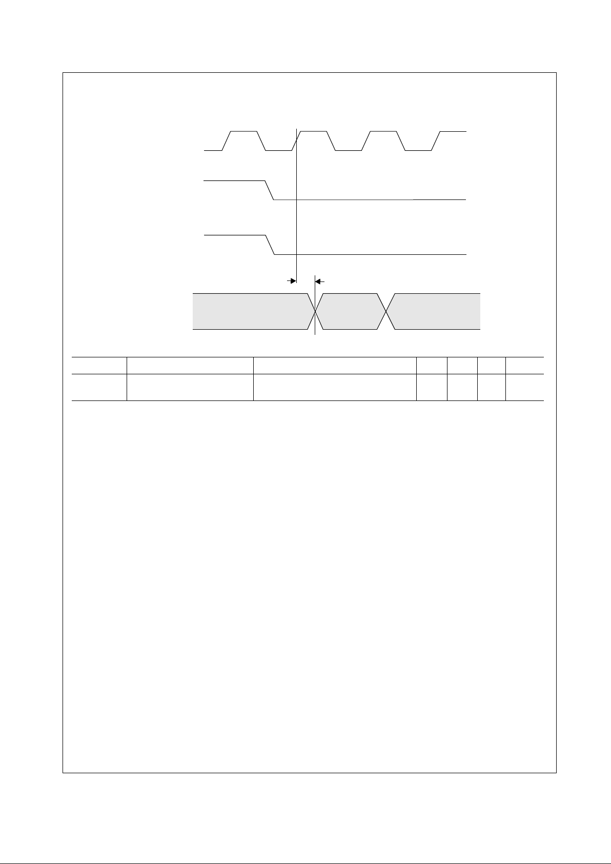
67 www.national.com
DP83848C
8.2.7 100BASE-TX Transmit Packet Deassertion Timing
Note: Deassertion is determined by measurin g the time from the first rising edge of TX_ CLK oc cu rrin g a fter the deassertion of TX_EN to the first bit o f the “T” cod e group as output from the PMD Output Pair . 1 bit ti me = 10 ns in 100 M b/s mode.
Parameter Description Notes Min Typ Max Units
T2.7.1 TX_CLK to PMD Output Pair
Deassertion
100 Mb/s Normal mode 6 bits
TX_CLK
TXD
TX_EN
PMD Output Pair
(T/R) DATA IDLE
T2.7.1
(T/R) DATA IDLE

68 www.national.com
DP83848C
8.2.8 100BASE-TX Transmit Timing (t
R/F
& Jitter)
Note: Normal Mismatch is the difference between the maximum and minimum of all rise and fall times
Note: Rise and fall times taken at 10% and 90% of the +1 or -1 amplitude
Parameter Description Notes Min Typ Max Units
T2.8.1 100 Mb/s PMD Output Pair tR
and t
F
3 4 5 ns
100 Mb/s tR and tF Mismatch 500 ps
T2.8.2 100 Mb/s PMD Output Pair
Transmit Jitter
1.4 ns
PMD Output Pair
T2.8.1
T2.8.1
T2.8.1
T2.8.1
+1 rise
+1 fall
-1 fall
-1 rise
eye pattern
T2.8.2
T2.8.2
90%
10%
10%
90%
PMD Output Pair

69 www.national.com
DP83848C
8.2.9 100BASE-TX Receive Packet Latency Timing
Note: Carrier Sense On Delay is determin ed by measuri ng the ti me fro m the first bit of the “J” code group to the asse rtion
of Carrier Sense.
Note: 1 bit time = 10 ns in 100 Mb/s mode
Note: PMD Input Pair voltage amplitude is greater than the Signal Detect Turn-On Threshold Value.
8.2.10 100BASE-TX Receive Packet Deassertion Timing
Note: Carrier Sense Off Delay is determined by measur ing th e time from the fir st bit o f the “T” c ode g roup to t he deas sertion of Carrier Sense.
Note: 1 bit time = 10 ns in 100 Mb/s mode
Parameter Description Notes Min Typ Max Units
T2.9.1 Carrier Sense ON Delay 100 Mb/s Normal mode 20 bits
T2.9.2 Receive Data Latency 100 Mb/s Normal mode 24 bits
Parameter Description Notes Min Typ Max Units
T2.10.1 Carrier Sense OFF Delay 100 Mb/s Normal mode 24 bits
CRS
RXD[3:0]
PMD Input Pair
RX_DV
RX_ER
IDLE
Data
T2.9.1
T2.9.2
(J/K)
CRS
T2.10.1
PMD Input Pair
DATA
IDLE
(T/R)

70 www.national.com
DP83848C
8.2.11 10 Mb/s MII Transmit Timing
Note: An attached Mac should drive the transmit signals using the positive edge of TX_CLK. As shown above, the MII
signals are sampled on the falling edge of TX_CLK.
8.2.12 10 Mb/s MII Receive Timing
Note: RX_CLK may be held low for a longer period of time during transition between reference and recovered clocks.
Minimum high and low times will not be violated.
Parameter Description Notes Min Typ Max Units
T2.11.1 TX_CLK High/Low Time 10 Mb/s MII mode 190 200 210 ns
T2.11.2 TXD[3:0], TX_EN Data Setup to TX_CLK fall 10 Mb/s MII mode 25 ns
T2.11.3 TXD[3:0], TX_EN Data Hold from TX_CLK rise 10 Mb/s MII mode 0 ns
Parameter Description Notes Min Typ Max Units
T2.12.1 RX_CLK High/Low Time 160 200 240 ns
T2.12.2 RX_CLK to RXD[3:0], RX_DV Delay 10 Mb/s MII mode 100 ns
T2.12.3 RX_CLK rising edge delay from RXD[3:0],
RX_DV Valid
10 Mb/s MII mode 100 ns
TX_CLK
TXD[3:0]
TX_EN
Valid Data
T2.11.2
T2.11.3
T2.11.1
T2.11.1
RX_CLK
RXD[3:0]
RX_DV
T2.12.2
T2.12.1
T2.12.1
T2.12.3
Valid Data

71 www.national.com
DP83848C
8.2.13 10 Mb/s Serial Mode Transmit Timing
8.2.14 10 Mb/s Serial Mode Receive Timing
Note: RX_CLK may be held high for a longer period of time during transition between reference and recovered clocks.
Minimum high and low times will not be violated.
Parameter Description Notes Min Typ Max Units
T2.13.1 TX_CLK High Time 10 Mb/s Serial mode 20 25 30 ns
T2.13.2 TX_CLK Low Time 10 Mb/s Serial mode 70 75 80 ns
T2.13.3 TXD_0, TX_EN Data Setup to TX_CLK rise 10 Mb/s Serial mode 25 ns
T2.13.4 TXD_0, TX_EN Data Hold from TX_CLK rise 10 Mb/s Serial mode 0 ns
Parameter Description Notes Min Typ Max Units
T2.14.1 RX_CLK High/Low Time 35 50 65 ns
T2.14.2 RX_CLK fall to RXD_0, RX_DV Delay 10 Mb/s Serial mode -10 10 ns
TX_CLK
TXD[0]
TX_EN
Valid Data
T2.13.3
T2.13.4
T2.13.1
T2.13.2
RX_CLK
RXD[0]
RX_DV
T2.14.2
T2.14.1
T2.14.1
Valid Data

72 www.national.com
DP83848C
8.2.15 10BASE-T Transmit Timi ng (Start of Packet)
Note: 1 bit time = 100 ns in 10Mb/s.
8.2.16 10BASE-T Transmit Timing (End of Packet)
Parameter Description Notes Min Typ Max Units
T2.15.1 Transmit Output Delay from the
Falling Edge of TX_CLK
10 Mb/s MII mode 3.5 bits
T2.15.2 Transmit Output Delay from the
Rising Edge of TX_CLK
10 Mb/s Serial mode 3.5 bits
Parameter Description Notes Min Typ Max Units
T2.16.1 End of Packet High Time
(with ‘0’ ending bit)
250 300 ns
T2.16.2 End of Packet High Time
(with ‘1’ ending bit)
250 300 ns
TX_CLK
TX_EN
TXD
PMD Output Pair
T2.15.1
T2.15.2
TX_CLK
TX_EN
PMD Output Pair
00
11
PMD Output Pair
T2.16.1
T2.16.2

73 www.national.com
DP83848C
8.2.17 10BASE-T Receive Timing (Start of Packet)
Note: 10BASE-T RX_DV Latency is measured from first bit of preamble on the wire to the assertion of RX_DV
Note: 1 bit time = 100 ns in 10 Mb/s mode.
8.2.18 10BASE-T Receive Timing (End of Packet)
Parameter Description Notes Min Typ Max Units
T2.17.1 Carrier Sense Turn On Delay (PMD
Input Pair to CRS)
630 1000 ns
T2.17.2 RX_DV Latency 10 bits
T2.17.3 Receive Data Latency Measurement sh own from SFD 8 bits
Parameter Description Notes Min Typ Max Units
T2.18.1 Carrier Sense Turn Off Delay 1.0 µs
TPRD±
CRS
RX_CLK
RX_DV
1st SFD bit decoded
RXD[3:0]
T2.17.1
T2.17.2
T2.17.3
101010101011
Preamble SFD Data
0000
1
0
1
PMD Input Pair
RX_CLK
CRS
IDLE
T2.18.1

74 www.national.com
DP83848C
8.2.19 10 Mb/s Heartbeat Timing
8.2.20 10 Mb/s Jabber Ti ming
Parameter Description Notes Min Typ Max Units
T2.19.1 CD Heartbeat Delay All 10 Mb/s modes 1200 ns
T2.19.2 CD Heartbeat Duration All 10 Mb/s modes 1000 ns
Parameter Description Notes Min Typ Max Units
T2.20.1 Jabber Activation Time 85 ms
T2.20.2 Jabber Deactivation Time 500 ms
TX_CLK
TX_EN
COL
T2.19.1
T2.19.2
TXE
PMD Output Pair
COL
T2.20.2
T2.20.1

75 www.national.com
DP83848C
8.2.21 10BASE-T Normal Link Pulse Timing
Note: These specifications represent transmit timings.
8.2.22 Auto-Negotiation Fast Link Pulse (FLP) Timing
Note: These specifications represent transmit timings.
Parameter Description Notes Min Typ Max Units
T2.21.1 Pulse Width 100 ns
T2.21.2 Pulse Period 16 ms
Parameter Description Notes Min Typ Max Units
T2.22.1 Clock, Data Pulse Width 100 ns
T2.22.2 Clock Pulse to Clock Pulse
Period
125 µs
T2.22.3 Clock Puls e to Data Puls e
Period
Data = 1 62 µs
T2.22.4 Burst Width 2 ms
T2.22.5 FLP Burst to FLP Burst Period 16 ms
T2.21.2
T2.21.1
Normal Link Pulse(s)
clock
pulse
data
pulse
clock
pulse
FLP Burst FLP Burst
Fast Link Pulse(s)
T2.22.1
T2.22.1
T2.22.2
T2.22.3
T2.22.4
T2.22.5

76 www.national.com
DP83848C
8.2.23 100BASE-TX Signal Detect Timing
Note: The signal amplitude on PMD Input Pair must be TP-PMD compliant.
8.2.24 100 Mb/s Internal Loopback Timing
Note1: Due to the nature of the descrambler function, all 100BASE-TX Loopback modes will cause an initial “dead-time”
of up to 550 µs during which time no data will be present at the receive MII outputs. The 100BASE-TX timing specified is
based on device delays after the initial 550µs “dead-time”.
Note2: Measurement is made from the first rising edge of TX_CLK after assertion of TX_EN.
Parameter Description Notes Min Typ Max Units
T2.23.1 SD Internal Turn-on Time 1 ms
T2.23.2 SD Internal Turn-off Time 350 µs
Parameter Description Notes Min Typ Max Units
T2.24.1 TX_EN to RX_DV Loopback 100 Mb/s internal loopback mode 240 ns
T2.23.1
SD+ internal
T2.23.2
PMD Input Pair
TX_CLK
TX_EN
TXD[3:0]
CRS
RX_CLK
RXD[3:0]
RX_DV
T2.24.1

77 www.national.com
DP83848C
8.2.25 10 Mb/s Internal Loopback Timing
Note: Measurement is made from the first rising edge of TX_CLK after assertion of TX_EN.
Parameter Description Notes Min Typ Max Units
T2.25.1 TX_EN to RX_DV Loopback 10 Mb/s internal loopback mode 2 µs
TX_CLK
TX_EN
TXD[3:0]
CRS
RX_CLK
RXD[3:0]
RX_DV
T2.25.1

78 www.national.com
DP83848C
8.2.26 RMII Transmit Timing
Parameter Description Notes Min Typ Max Units
T2.26.1 X1 Clock Period 50 MHz Reference Clock 20 ns
T2.26.2 TXD[1:0], TX_EN, Data Setup
to X1 rising
4 ns
T2.26.3 TXD[1:0], TX_EN, Data Hold
from X1 rising
2 ns
T2.26.4 X1 Clock to PMD Output Pair
Latency
From X1 Rising edge to first bit of symbol 17 bits
X1
TXD[1:0]
TX_EN
Valid Data
T2.26.2
T2.26.3
T2.26.1
PMD Output Pair
Symbol
T2.26.4

79 www.national.com
DP83848C
8.2.27 RMII Receive Timing
Note: Per the RMII Specification, output delays assume a 25pF load.
Note: CRS_DV is asserted asynchronously in order to minim ize laten cy of control signals throug h the why. CRS_DV may
toggle synchronously at the end of the packet to indicate CRS deassertion.
Note: RX_DV is synchronous to X1. While not p art of the RM II spec ifica tion, th is sig nal is prov ided to simpl ify recov ery of
receive data.
Parameter Description Notes Min Typ Max Units
T2.27.1 X1 Clock Period 50 MHz Reference Clock 20 ns
T2.27.2 RXD[1:0], CRS_DV, RX_DV,
and RX_ER output delay from
X1 rising
2 14 ns
T2.27.3 CRS ON delay From JK symbol on PMD Receive Pair to
initial assertion of CRS_DV
18.5 bits
T2.27.4 CRS OFF delay From TR symbol on PMD Receive Pair to
initial deassertion of CRS_DV
27 bits
T2.27.5 RXD[1:0] and RX_ER latency From symbol on Receive Pair. Elasticity
buffer set to default value (01)
38 bits
CRS_DV
X1
RXD[1:0]
RX_ER
T2.27.2
T2.27.1
T2.27.2
PMD Input Pair
IDLE
Data
(J/K)
T2.27.3
T2.27.5
Data
(TR)
T2.27.4
RX_DV
T2.27.2
T2.27.2

80 www.national.com
DP83848C
8.2.28 Isolation Timing
8.2.29 25 MHz_OUT Timing
Note: 25 MHz_OUT characteristics are dependent upon the X1 input characteristics.
Parameter Description Notes Min Typ Max Units
T2.28.1 From software clear of bit 10 in
the BMCR register to the transition from Isolate to Normal Mode
100 µs
T2.28.2 From Deassertion of S/W or H/W
Reset to transition from Isolate to
Normal mode
500 µs
Parameter Description Notes Min Typ Max Units
T2.29.1 25 MHz_OUT High/Low Time MII mode 20 ns
RMII mode 10 ns
T2.29.2 25 MHz_OUT propagation delay Relative to X1 8 ns
Clear bit 10 of BMCR
(return to normal operation
from Isolate mode)
H/W or S/W Reset
(with PHYAD = 00000)
MODE
ISOLATE
NORMAL
T2.28.2
T2.28.1
X1
T2.29.2
25 MHz_OUT
T2.29.1 T2.29.1

81 www.national.com
DP83848C
NOTES:

DP83848C PHYTER
®
— Commercial Temperature Single Port 10/100 Mb/s Ethernet Physical Layer Transceiver
inches (millimeters) unless otherwise noted
National does not assume any responsibility for use of any circuitry described, no circuit patent licenses are implied and National reserves the right at any time without notice to change said circuitry and specifications.
LIFE SUPPORT POLICY
NATIONAL’S PRODUCTS ARE NOT AUTHORIZED FOR USE AS CRITICAL COMPONENTS IN LIFE SUPPORT
DEVICES OR SYSTEMS WITHOUT THE EXPRESS WRITTEN APPROVAL OF THE PRESIDENT AND GENERAL
COUNSEL OF NATIONAL SEMICONDUCTOR CORPORATION. As used herein:
1. Life support devices or systems are devices or systems which,
(a) are intended for surgical implant into the body, or (b) support
or sustain life, and whose failure to perform, when properly used
in accordance with instructions for use provided in the labeling,
can be reasonably expected to result in a significant injury to the
user.
2. A critical component is any component of a life support device
or system whose failure to perform can be reasonably expected
to cause the failure of the life support device or system, or to affect its safety or effectiveness.
National Semiconductor
Corporation
Tel: 1-800-272-9959
Fax: 1-800-737-7018
Email: support@nsc.com
National Semiconductor
Europe
Fax: +49 (0) 180-530 85 86
Email: europe.sup port@nsc.com
Deutsch Tel: +49 (0) 69 9508 6208
English Tel: +44 (0) 870 24 0 2171
Francais Tel: +33 (0) 1 41 91 8790
National Semiconductor
Japan Lt d.
Tel: 81-3-5639-7560
Fax: 81-3-5639-7507
www.national.com
National Semiconductor
Asia Pacific
Customer Response Group
Tel: 65-254-4466
Fax: 65-250-4466
Email: ap.support@nsc.com
BANNED SUBSTANCE COMPLIANCE
National Semiconductor certifies that the products and packing materi als meet the provisions of the Customer Products Stewardship
Specification (CSP-9-111C2) and the Banned Substances and Materials of Interest Specification (CSP-9-111S2) and contain no “Banned
Substances” as defined in CSP-9-111S2.
Leadfree products are RoHS compliant.
9.0 Physical Dimensions
Lead Quad Frame Package (LQFP)
NS Package Number VBH48A
 Loading...