

NSC DP83820BVUW-AB, DP83820BVUW Datasheet
DP83820 10/100/1000 Mb/s PCI Ethernet Network Interface Controller
© 2001 National Semiconductor Corporation
www.national.com
PRELIMINARY
February 2001
DP83820 10/100/1000 Mb/s PCI Ethernet Network Interface
Controller
General Description
DP83820 is a single-chip 10/100/1000 Mb/s Ethernet
Controller for the PCI bus. It is targeted at highperformance adapter cards and mother boards. The
DP83820 full y implements the V2.2 66 MHz, 64-bit PCI bus
interface for host communications with power management
support. Packet descriptors and data are transferred via
bus-mastering, reducing the burden on the host CPU. The
DP83820 can support full duplex 10/100/1000 Mb/s
transmission and reception.
Features
— IEEE 802.3 Compliant, 66/33 Mhz, 64/32-bit PCI V2.2
MAC/BIU support s data rates from 1 Mb/s t o 1000 Mb/s.
This allows support for traditional 10 Mb/s Ethernet, 100
Mb/s Fast Ethernet, as well as 1000 Mb/s Gigabit
Ethernet.
— Flexible, pr ogr ammable Bus master - b urst s izes of up to
256 dwords (1024 bytes)
— BIU compliant with PC 97 and PC 98 Hardware Design
Guides, PC 99 Ha rdware De si gn Guide draft , ACP I v1.0 ,
PCI Power Management Specification v1, OnNow
Device Class Power Management Reference
Specificat ion - Network Device Class v1.0a
— Wake on LAN (WOL) support compliant with PC98,
PC99, and OnNow, including directed packets, Magic
Packet with SecureOn, ARP packets, pattern match
packets, and Phy status change
— GMII/MII provides IEEE 802.3 standard interface to
support 10/100/ 1000 Mb/s physical layer devices
— Ten-Bit Interface (TBI) for support of 1000BASE-X
— Virtual LAN (VLAN) and long frame support. VLAN tag
insertion support for transmit packets. VLAN tag
detection and removal for receive pack ets
— 802.3x Full duplex flow control, including automatic
transmission of Pause frames based on Rx FIFO
thresholds
— IPv.4 checksum task off-loading. Supports checksum
generation an d veri fic ation of I P, TCP, a nd UDP head ers
— 802.1D and 802.1Q priority queueing support. Supports
multiple priority queues in both transmit and receive
directions.
— Extremely flexible Rx packet filtration including: single
address perfect filter with MSb masking, broadcast,
2,048 entry multicast/unicast hash table, deep packet
pattern matching for up to 4 unique patterns.
— Statistics gathered for support of RFC 1213 (MIB II),
RFC 1398 (Ether-like MIB), IEEE 802.3 LME, reducing
CPU overhead for management.
— Internal 8 KB Transmit and 32 KB Receive data FIFOs
— Supports Jumbo packets
— Serial EEPROM port with auto-load of configuration data
from EEPROM at power-on
— Flash/PROM interface for remote boot support
— Full Duplex support for 10/100/1000 Mb/s data rates
— 208-pin PQFP package
— Low power CMOS design
— 3.3V powered I/Os with 5V tolerant inputs
— JTAG Boundary Scan supported
System Diagram
PCI Bus
DP83820
EEPROM (optional)
10/100/1000 Mb/s
PHY
Boot ROM (optional)
MII
GMII

2
www.national.com
1.0 Connection Diagram
Order Number DP83820VUW
See NS Package Number NVUW208A
AD16
CBEN2
PCIVSS
FRAMEN
IRDYN
TRDYN
PCIVDD
DEVSELN
STOPN
PERRN
SERRN
PAR
CBEN1
AD15
AD14
PCIVSS
AD13
AD12
AD11
PCIVDD
AD10
AD9
AD8
CBEN0
AD7
AD6
PCIVSS
AD5
AD4
PCIVDD
AD3
AD2
AD1
AD0
ACK64N
PCIVSS
REQ64N
CBEN7
CBEN6
PCIVDD
CBEN5
CBEN4
PAR64
AD63
AD62
PCIVSS
AD61
AD60
AD59
AD58
PCIVDD
AD57
MD7
MD6
MD5
MD4/EEDO
VDDIO
VSSIO
MD3
MD2
MD1/CFGDISN
MD0/PMGDISN
MWRN
MRDN
MCSN
EESEL
RESERVED
COREVDD
COREVSS
CLKRUNN
3VAUX
PWRGOOD
PCIVIO
AD32
AD33
AD34
PCIVDD
AD35
AD36
AD37
PCIVSS
AD38
AD39
AD40
AD41
PCIVDD
AD42
AD43
AD44
AD45
PCIVSS
AD46
AD47
AD48
AD49
AD50
PCIVDD
AD51
AD52
AD53
PCIVSS
AD54
AD55
AD56
RXD0
RXD1
RXD2
RXD3
VSSIO
VDDIO
RXD4
RXD5
RXD6
RXD7
RXDV/RXD8
RXER/RXD9
CRS/SIG_DET
COL
RXEN
PHYRSTN
COREVSS
COREVDD
PMEN
PCICLK
TRSTN
TCK
TMS
TDO
TDI
PCIVSS
INTAN
RSTN
GNTN
REQN
PCIVDD
AD31
AD30
AD29
AD28
AD27
AD26
AD25
AD24
PCIVSS
CBEN3
IDSEL
AD23
AD22
PCIVDD
AD21
AD20
AD19
COREVSS
COREVDD
AD18
AD17
157
158
159
160
161
162
163
164
165
166
167
168
169
170
171
172
173
174
175
176
177
178
179
180
181
182
183
184
185
186
187
188
189
190
191
192
193
194
195
196
197
198
199
200
201
202
203
204
205
206
207
208
123456789101112131415161718192021222324252627282930313233343536373839404142434445464748495051
52
104
103
102
101
100
99
98
97
96
95
94
93
92
91
90
89
88
87
86
85
84
83
82
81
80
79
78
77
76
75
74
73
72
71
70
69
68
67
66
65
64
63
62
61
60
59
58
57
56
55
54
53
156
155
154
153
152
151
150
149
148
147
146
145
144
143
142
141
140
139
138
137
136
135
134
133
132
131
130
129
128
127
126
125
124
123
122
121
120
119
118
117
116
115
114
113
112
111
110
109
108
107
106
105
DP83820
Gigabit NIC
RXCLK/RXPMACLK1
TXCLK/RXPMACLK0
TXER/TXD9
TXEN/TXD8
TXD7/MA15
TXD6/MA14
VDDIO
VSSIO
TXD5/MA13
TXD4/MA12
TXD3/MA11
TXD2/MA10
VDDIO
VSSIO
TXD1/MA9
TXD0/MA8
GTXCLK/TXPMACLK
MDIO
MDC
REF125
VDDIO
VSSIO
SPD1000
SPD100
PHYLNK
GP1DUP
GP5
GP4
GP3
GP2
RESERVED
AVDD
AVSS
OSCVDDX1X2
OSCVSS
RESERVED
RESERVED
RESERVED
COREVDD
COREVSS
MA7
MA6
MA5
VDDIO
VSSIO
MA4/EECLK
MA3/EEDI
MA2
MA1
MA0

3
www.national.com
2.0 Pin Descriptions
PCI In t e r f a c e
Symbol Pin No(s) Direction Descripti on
AD31-0 188, 189, 190 ,
191, 192, 193 ,
194, 195, 199 ,
200, 202, 203 ,
204, 207, 208 ,
1, 14, 15, 17,
18, 19, 21, 22,
23, 25, 26, 28,
29, 31, 32, 33,
34
I/O
Address and Data:
Multipl exed address an d da ta bus. As a bus ma s t er, the
DP83820 will drive address during the first bus phase. During subsequent
phases, the DP8 3820 will either read or write dat a exp ecting the target to
increment its address po inter. As a bus target, the DP83820 will decode each
address on the bus and respond if it is the target being addressed.
CBEN3-0 197, 2, 13, 24 I/O
Bus Command/Byte Enable:
During the address phase these signals define
the “bus command” or the type of bus tr an sac ti on t ha t wil l tak e pl ace . D uri ng the
data phase these pins in dicate which byte lanes contain valid data. CBEN0
applie s to byte 0 (bits 7-0) and C BEN3 applies to byte 3( bits 31-24).
PCICLK 176 I
Clock:
This PCI Bus clock provi des timing for all bus phases. The rising edge
defines the start of each phase. The cl ock frequency ranges from 0 to 66 MHz.
DEVSELN 8 I/O
Device Selec t:
As a target, the DP8382 0 asserts this signal low when it
recognizes its address after FRAMEN is asserted. As a bus master, the
DP83820 samples this signal to insure that the destination address for the data
transfer is recognized by a PCI target.
FRAMEN 4 I/O
Frame:
As a bus master, this signal is asserted low to indicate the beginning
and duration of a bus transac tion. Data transfe r takes place when this s ignal is
asserted. I t is de-asserted before th e transaction i s in its final phase. As a
target, the device monitors this signal before decoding the address to check if
the current transaction is addressed to it.
GNTN 185 I
Grant:
This signal is asserted low to indicate to the DP83820 that it has been
granted ownership of the bus by the central arbiter. This input is used when the
DP83820 is acting as a bus master.
IDSEL 198 I
Initialization Device Select:
This pin is sampled by the DP83820 to identify
when configuration read and write accesses are in tended for it.
INTAN 183 O
Interrupt A:
This signal is asserted low w hen an interrupt condition as defined
in the Interrupt Status Register, Interrupt Mask, and Interrupt Enable registers
occurs.
IRDYN 5 I/O
Initiator Ready:
As a bus master, this signal will be asserted low when the
DP83820 is ready to complete the current data phase transaction. This signal is
used in conjunction with the T RYDN signal. Data transaction ta kes place at t he
rising edge of PCICLK when both IRDY N and TRDYN are asserted low. As a
target, this signal indicates that the master has put the data on the bus.
PAR 12 I/O
Parity:
This sign al in di cate s even parity acr o ss AD 31 -0 an d CB EN 3-0 inc lu ding
the PAR pin. As a master, PAR is asserted during address and write data
phases. As a target, PAR is asserted during read data phases.
PERRN 10 I/O
Parity Error:
The DP83820 as a master or target will assert this signal low to
indica te a pa rity er ror on an y in com ing d at a (e xc ep t for special c ycl es ). As a bus
master, it will monitor this signal on all write operations (except for special
cycles).
REQN 186 O
Request:
The DP83 820 will assert this signal low to request the owner s hip of
the bus to the central arbiter.
RSTN 184 I
Reset:
When this signa l is asserted all outp uts of DP83820 will be tri-stated
and the device will be put into a known state.

4
www.national.com
2.0 Pin Descr iptions
(Continued)
SERRN 11 I/O
System Error :
This signal is asserted low by DP83820 during address parity
errors and system errors if enabled.
STOPN 9 I/O
Stop:
This signal is asserted low by the target device to request the master
device to stop the current transaction.
TRDYN 6 I/O
Target Ready:
As a target, this signal will be asserted low when the (slave)
device is re ad y to complet e the cu r rent data ph as e tr an sa c tion. This sig na l is
used in co njunction with the IRDYN signal . Data transaction tak es place at the
rising edge of PCICLK when both IRDYN and TRDYN are asserted low. As a
master, this signal indicates that the target is ready for the data during write
operation and with the data during read operation.
PMEN 175 O
Power Management Event:
This signal is asserted low by DP83820 to indicate
that a power management event has occurred.
3VAUX 86 I
PCI Aux Voltage Sense:
This pin is used to sense the presence of a 3.3v
auxiliary supply in order to define the PME Support available.
This pi n pad has an internal weak pull down.
PWRGOOD 85 I
PCI bus power good:
Connected to PCI bus 3.3v power, this pin is used to
sense the presence of PCI bus power during the D3 power management st ate.
This pi n pad has an internal weak pull down.
CLKRUNN 87 I/O
Clockrun
: This signal is asserted low by DP83820 to indicate that a Clockrun
Event has occurred.
AD63-32 44, 45, 47, 48,
49, 50, 52, 53,
54, 55, 57, 58,
59, 61, 62, 63,
64, 65, 67, 68,
69, 70, 72, 73,
74, 75, 77, 78,
79, 81, 82, 83
I/O
64-bit Extension Address and Data:
Multiplexed addr ess and data bus.
Provides upper address bits during 64-bit DAC command. During data phase,
used for transferring upper 32-bits of a 64-bit data transaction.
CBEN7- 4 38, 39, 41, 42 I/O
64-bit Extension Bus Command/Byte Enables:
During the address phase
these signals define the “bus command” for a 64-bit DAC comman d. During a
64-bit data phase these pins indicate which byte lanes contain valid data.
CBEN4 applies to byte 4(bits 39-32) and CBEN7 applies to byte 7(bits 63-56).
REQ64N 37 I/O
Request 64-bit Transfer:
The DP83 820 will assert this signal low to request a
64-bit transfer of data. This pin is sampled by the DP83820 during reset to
determine if the device is connected to a 64-bit datapath.
ACK64N 35 I
Acknowledge 64-bit Transfer:
The DP83820 will samples this signal on bus
master cyc le s whe n i t h as re qu este d a 6 4-b it da ta transfer . If bo t h RE Q64 N and
ACK64N are asserted, the n a 64-bit transfer will be per formed. As a target, the
DP83820 only supports 32-bit transfers, so it will never assert ACK64N.
PAR64 43 I/O
Parity Upper DWORD:
This signal indicates even parity across AD63-32 and
CBEN7-4 including the PAR64 pin. As a master, PAR64 is driven during
address and write data phases. As a target, the DP83820 only supports 32-bit
transfers, so it will not drive PAR64.
PCIVIO 84 I
PCI Bu s VIO:
This pin should be connected to the VIO pins of the PCI bus. It
provides a direct connection to the ESDPLUS ring for biasing. It may be
connected to 5V if available. It should not be connected to 3.3V unless all
signal ing i s 3 .3 V as th is w ill in te rfere with 5V tol er anc e . C ar e s ho ul d be t aken in
connecting this to power supplies when power management functions are
enabled.
PCI In t e r f a c e
Symbol Pin No(s) Direction Descripti on

5
www.national.com
2.0 Pin Descr iptions
(Continued)
Media Independent Interface (MII) - and Gigabit Media Independent Interface (GMII).
Symbol Pin No(s) Direction Description
COL 170 I
Collision Detect:
The COL signal is asserted high asynchronously by the
external PMD upon detection of a collision on the medium. It will remain
asserted as long as the collision condition persists.
CRS/SIGDET 169 I
Carrier Sense:
This signal is asserted high a synchronously by the external
physical un it up on dete c t io n of a non - id le med iu m .
Signal Dete ct:
In TBI mode , this signal is used to bring in the Signal Detect
indication from the Phy.
MDC 138 O
Management Data Clock:
Clock signal with a maximum rate of 2.5 MHz used
to transfer management data for the external PMD on the MDIO pin.
MDIO 139 I/O
Management Data I/O:
Bidirectional signal used to transfer management
information for the external PMD. Requires an external 4.7 KΩ pullup resistor.
RXCLK/
RXPMACLK1
156 I
Receive Clock:
A continuous clock, sourced by an external PMD device, that is
recovered from the incoming data. Duri ng 1000 Mb/s mode RX_C LK is 125
MHz, during 100 Mb/s operation RX_CLK i s 25 MHz and during 10 Mb/s this is
2.5 MHz.
Receive PMA Clock 1:
In TBI mode, this 62.5Mhz clock is used in conjunction
with RXP MA C LK0 to clo c k 10- b it TB I data in to the D P83 82 0. The r is in g edge of
RXPMAC LK1 clocks the even-numbered bytes .
RXD7,
RXD6,
RXD5,
RXD4,
RXD3,
RXD2,
RXD1,
RXD0
166,
165,
164,
163,
160,
159,
158,
157
I
Gigabit Receive Data:
This is a group of 8 signal s, sourced from an external
PMD, that contains data aligned on byte boundaries and are driven
synchronous to the RX_CLK. RXD7 is most signif icant bit.
Receive Data:
This is a group of 4 signals, sourced from an external PMD, that
contains data aligned on nibble boundaries and are driven synchronous to the
RX_CLK. RXD3 is the most significant bit and RXD0 is the least significant bit.
RXD7 through RXD4 are not used in this mode.
TBI Receive Data:
In TBI mode, these bits are the lower 8 bits of the 10-bit TBI
Receive data.
RXDV/RXD8 167 I
Receive Data Valid:
This indicates that the external PMD is presenting
recovered and decoded nibbles on the RXD signals, and that RX _CLK is
synchronous to the recovered data in 10 0 Mb/s operation. This signal will
encompass the frame, starting with the Start-of-Frame delimiter (JK) and
excluding any End-of-Frame delimiter (TR).
TBI Receive Data:
In TBI mode, this is RXD8 of the 10-bit TBI Receive data.
RXER/RXD9 168 I
Receive Error:
This signal is asserted high synchronously by the external PMD
whenever it detects a media error and RXDV is asserted in 100 Mb/s or 1000
Mb/s op era tion.
TBI Receive Data:
In TBI mode, this is RXD9 of the 10-bit TBI Receive data.
RXEN 171 O
Receive Output Enable:
This pin is used t o disable an external PMD while the
BIOS ROM is being accessed.
TXCLK/
RXPMACLK0
155 I
MII Transmit Clock:
A continuous clock that is sourced by the external PMD.
During 100 Mb/s operation this is 25 MHz +/- 100 ppm. During 10 Mb/s
operation this clock is 2.5 MHz +/- 100 ppm.
Receive PMA Clock 0:
In TBI mode, this 62.5Mhz clock is used in conjunction
with RXP MA C LK1 to clo c k 10- b it TB I data in to the D P83 82 0. The r is in g edge of
RXPMAC LK0 clocks the odd-numbered bytes.

6
www.national.com
2.0 Pin Descr iptions
(Continued)
TXD7/MA15,
TXD6/MA14,
TXD5/MA13,
TXD4/MA12,
TXD3/MA11,
TXD2/MA10,
TXD1/MA9,
TXD0/MA8
152,
151,
148,
147,
146,
145,
142,
141
O
Gigabit Transmit Data:
This is a group of 8 signa ls which are driven
synchronous to GTXCLK. TXD7 is the most significant bit.
Transmit Data:
This is a group of 4 dat a signals which are driven synchronous
to the TXCLK for transmission to the external PMD. TXD3 is the most significant
bit and T XD0 is th e l east si gn i fica nt bi t. T X D7 t hro ug h T XD4 a r e no t use d i n th is
mode
TBI Transmit Data:
In TBI mode, this is the lower 8 bits of the 10-bit TBI
Transmit data.
BIOS ROM Address
: During external BIOS ROM access, these signals
become part of the RO M address.
TXEN/TXD8 153 O
Transmit Enab le:
This signal is synchronous to TXCLK and provides precise
framing for data carried on TXD3-0 for the external PMD. It is asserted when
TXD3- 0 co ntains valid da ta to be transmi tte d.
TBI Transmit Data:
In TBI mode, this is TXD8 of the 10-bit TBI Transmit data.
TXER/TXD9 154 O
Transmit Error:
This signal is synchronous to TXCLK and provides error
indications and also is used for 1000 Mb/s half-duplex carrier extension and
pack et b ur st ing fu nc ti ons . Th e DP838 20 wil l on ly as se rt thi s s ig nal i n 10 00 Mb/s
mode of operation.
TBI Transmit Data:
In TBI mode, this is TXD9 of the 10-bit TBI Transmit data.
GTXCLK/
TXPMACLK
140 O
GMII transmit Cl ock:
A continuous clock used for 1000 Mb/s. It is output to an
external PMD and is the reference clock for Tr ansmit GMII signaling. The clock
frequency is 125 MHz.
TBI Transmit Cl ock:
In TBI mode, this is the 125MHz transmit clock to an
external PMD and is the reference for Transmit TBI signaling.
REF125 137 I
125 MHz Reference Clock:
May be optionally connected to a 125 MHz
oscillator for 1000 Mb/s mode. If not used should be tied high.
BIOS ROM/Flash Interface
Symbol Pin No(s) Direction Description
MCSN 92 O
BIOS PROM/Flash Chip Select:
During a BIOS ROM/Flash access, this
signal is used to select the R OM device.
MD7, MD6,
MD5, MD4/EEDO,
MD3, MD2,
MD1/CFGDISN,
MD0/PMGDISN
104, 103,
102, 101,
98, 97,
96,
95,
I/O
BIOS ROM/Flash Data Bus:
During a BIOS ROM/Flash access these
signals are used to transfer data to or from the ROM/Flash device.
MD5:0 and MD7 pin p ads have an in ternal weak pull up.
MD6 pin pad has an internal weak pull down.
MA15/TXD7,
MA14/TXD6,
MA13/TXD5,
MA12/TXD4,
MA11/TXD3,
MA10/TXD2,
MA9/TXD1,
MA8/TXD0,
MA7, MA 6,
MA5, MA 4/EECLK ,
MA3/E ED I, MA 2,
MA1, MA 0
152,
151,
148,
147,
146,
145,
142,
141,
114, 113,
112, 109,
108, 107,
106, 105
O
BIOS ROM/Flash Address:
During a BIOS ROM/Flash access, these
signals are used to drive the ROM/Flash address.
Media Independent Interface (MII) - and Gigabit Media Independent Interface (GMII).
Symbol Pin No(s) Direction Description

7
www.national.com
2.0 Pin Descr iptions
(Continued)
Note: DP83820 supports NM27LV010 for the R O M interface device.
MWRN 94 O
BIOS ROM/Flash Write:
During a BIOS ROM/Flash access, this signal is
used to e nable data to be written to the Flash devi ce.
MRDN 93 O
BIOS ROM/Flash Read:
During a BIOS ROM/Flash access, this signal is
used to e nable data to be r ead from the Fla s h device.
Clock Interface
Symbol Pin No(s) Direction Description
X1 122 I
Crystal/Oscillator Input:
This pin is the primary clock reference input for the
DP83820 IC and must be connected to a 25MHz 0.005% (50ppm) clock source.
The DP83820 device supports either an external crystal resonator connected
across pins X1 and X2, or an external CMOS-level oscillator source connected
to pin X1 only.
X2 121 O
Crystal Output:
This pin is us ed in conj u ncti on wit h t he X1 p in to c onnec t t o a n
external 25MHz crystal resonator device. This pin must be left unconnected if
an external CMOS oscillator clock source is utilized. For more information see
the definition for pin X1.
Phy And General Purpose Interface
Symbol Pin No(s) Direction Descripti on
GP1DUP 131 I/O
General Purpose Pin 1 or Duplex Status:
By default, this pin ca n be used to
input the Full Duplex status from an external Phy. The pin can also be
programmed as a general purpose I/O. This pin pad has an internal weak pull
up.
GP2 127 I/O
General Purpose Pin 2:
This pi n is a general purpose I/O pin that can be
programmed as an input or output. This pin has an internal weak pull up.
GP3 128 I/O
General Purpose Pin 3:
This pi n is a general purpose I/O pin that can be
programmed as an input or output. This pin has an internal weak pull up.
GP4 129 I/O
General Purpose Pin 4:
This pi n is a general purpose I/O pin that can be
programmed as an input or output. This pin has an internal weak pull up.
GP5 130 I/O
General Purpose Pin 5:
This pi n is a general purpose I/O pin that can be
programmed as an input or output. This pin has an internal weak pull up.
PHYLNK 132 I
Phy L i nk S ta tus :
This ca n be us ed to in pu t th e Ph y Li nk S tat u s. Thi s a ll o ws t he
valu e to be read back from the MAC register space.
SPD100 133 I
100 Mb/s Speed Status:
This can be used to in pu t t he 100 Mb/ s S pee d Sta tus
from an external phy. This is used along with the SPD1000 bit to determine
current speed status of the Phy.
SPD1000 134 I
1000 Mb/s Speed Status:
This can be used to input the 1000 Mb/s Speed
Status from an external phy. This is used along with the SPD100 bit to
determine cu r rent spee d st atus of the Phy.
PHYRSTN 172 O
Phy Re set:
This pin can be used to reset an External Ph y.
BIOS ROM/Flash Interface
Symbol Pin No(s) Direction Description

8
www.national.com
2.0 Pin Descr iptions
(Continued)
Note: DP83820 supports NMC93C46 for the eeprom interface device.
Serial EEPROM Interface
Symbol Pin No(s) Direction Description
EESEL 91 O
EEPROM Chip Select:
This signal is used to enable the external EEPROM
device.
MA4/EECLK 109 O
EEPROM Clock:
During an EEPROM access (EESEL asserted), this pin is an
output used to drive the serial clock to an external EEPROM device.
MA3/EEDI 108 O
EEPROM Data In:
During an EEPROM access (EESEL asse r t ed ), this outpu t
is drives opcode, address, and data to an external serial EEPROM device.
MD4/EEDO 101 I
EEPROM Data Out:
During an EEPROM access (EESEL asserted), this pin is
an input used to retrieve EEPROM serial read data.
This pi n pad has an internal weak pull up.
JTAG Interface
Symbol Pin No(s) Direction Description
TCK 178 I Test Clock
TDI 181 I Test Data Input
TDO 180 O Test Output
TMS 179 I Test Mode Select
TRSTN 177 I Test Reset
Supply Pins
Symbol Pin No(s ) Direction Description
COREVD D 89, 116, 174, 206 S Mac/BIU digital core VDD - connect to Aux 1.8V supply VDD
COREVSS 88, 115, 173, 205 S Mac/BIU digital core VSS.
OSCVDD 123 S Oscillator VDD - connect to Aux 1.8V supply VDD
OSCVSS 120 S Oscillator VSS.
PCIVDD 187 , 201, 7, 20 , 30,
40, 51, 60, 71, 80
S PCI IO VDD - connect to PCI bus 3.3V VDD
PCIVSS 182, 196, 3, 16, 27,
36, 46, 56, 66, 76
S PCI IO VSS
VDDIO,
AVDD
100, 111, 136, 144,
150, 162, 12 5
S Misc. IO VD D, Analog VDD - connect to Aux 3.3V supply VDD
VSSIO,
AVSS
99, 110, 135, 143,
149, 161, 12 4
S Misc. IO VSS, Analog VSS
No Connects
Symbol Pin No(s) Direction Description
Reserved 90, 117, 118,
119, 126
This pin is reserved and cannot be connected to any external logic or net.
9
www.national.com
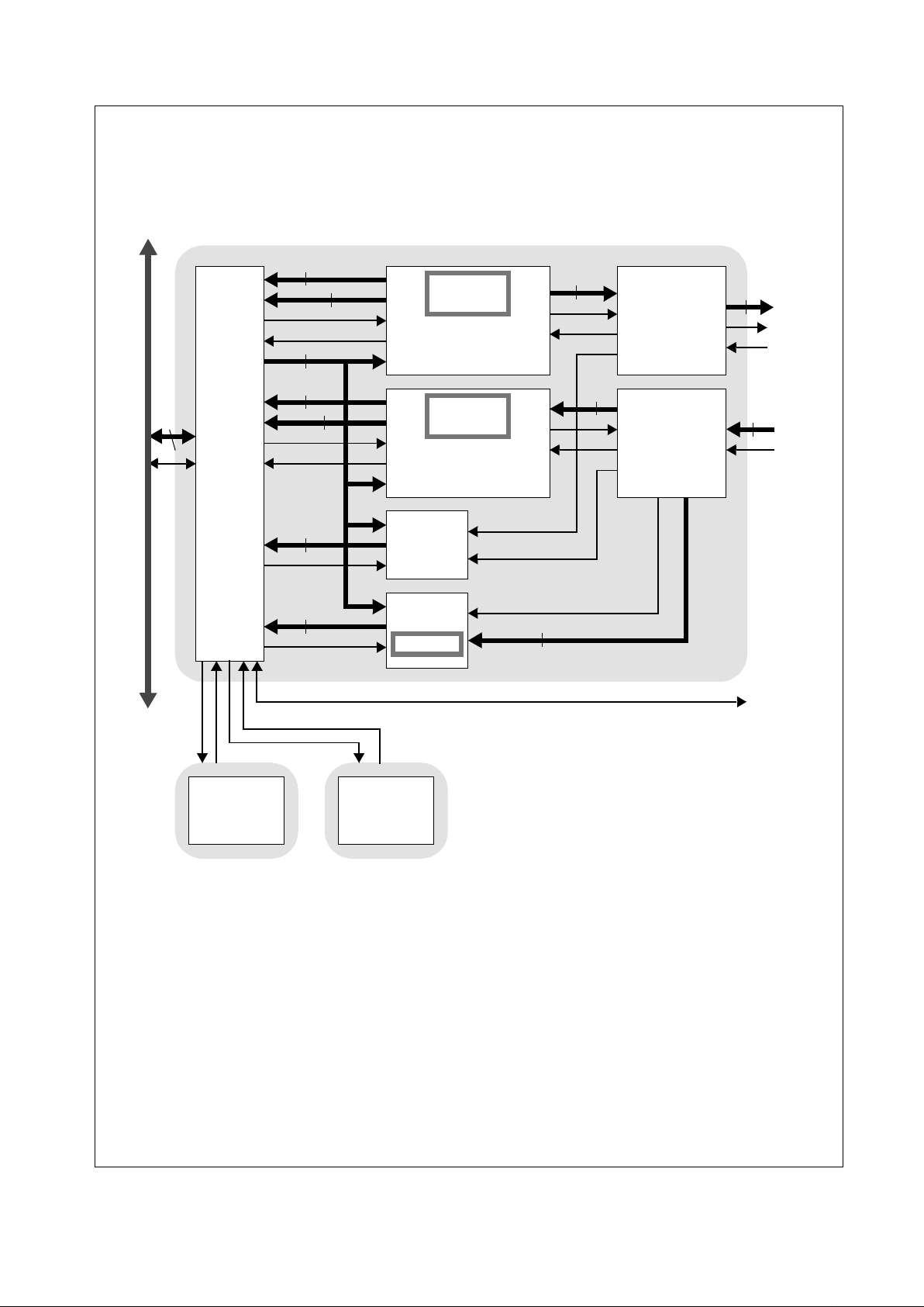
3.0 Functional Description
DP83820 consists of a PCI bus interface, BIOS ROM and
EEPROM interfaces, Receive and Transmit Data Buffer
Managers, an 802.3 Media Access Controller (MAC),
SRAM, and miscellaneous support logic.
Figure 3-1
DP83820
Functional Block Diagram
3.1 DP83820
The DP83820 device is an enhanced version of the NSC
MacPhyter MAC/BIU (Media Access Controller/Bus
Interface Unit) which has been modified for 1000 Mb/s
operation with additional buffering, higher bandwidth PCI
bus implementation, and the Gigabit Media Independent
Interface for 1000BASE-T phy support. The DP83820
supports an exter nal 10/100/1000 physical layer device.
DP83820 contains the following major design elements:
— a PCI bus interface,
— an EEPROM interface, for access to an NMC93C06
EEPROM,
— a buffer management scheme that is simple, efficient
and flexible,
— separate receive and transmit FIFOs and DMA
controllers,
— a 10/100/1000 Mb/s Ethernet Media Access Control
(MAC),
— a Physical Layer Interface (MII/GMII/TBI ),
— Management Information Base (MIB) Statistics
Registers,
— Receive Packet filteri ng logic.
This following section provides a functional overview of
interfaces of the DP83820.
Rx Filter
Tx Buffer Manager
Rx Buffer Manager
MIB
Tx MAC
Rx MAC
PCI BUS
PCI Bus
Interface
Data FIFO
Data FIFO
93C06
Serial
EEPROM
DP83820
32
15
64
32
64
32
32
64
64
64
8
8
64
Boot ROM/
Flash
MII
MGMT
SRAM
G/MII INTERFACE

3.0 Functional Description
(Continued)
10
www.national.com
3.2 PCI Bus Interface
The DP83820 implements the Peripheral Component
Interconnect (PCI) bus interface as defined in PCI Local
Bus Specification Version 2.2. When internal register are
being accessed the DP83820 acts as a PCI target (slave).
When accessin g host memory for descriptor or packet data
transfer, the DP83820 acts as a PCI bus master.
All required pins and functions are implemented. The
optional interface pin INTA for support of interrupt requests
is implemented as well . The b us inte rf ace also supports 64bit and 66Mhz operation in addition t o the more common
32-bit and 33-Mhz capabilities.
For more information, refer to the PCI Local Bus
Specification version 2.2, December 18, 1998.
3.2.1 Byte Ordering
The DP83820 can be configur ed to order the bytes of data
on the AD[31:0] bus to conform to Little Endian or Big
Endian ordering through the use of the CFG:BEM bit. Byte
ordering only affects bus mastered packet data transfers in
32-bit mode. Register infor mation remains bit aligned (i.e.
AD[31] maps to bi t 31 in any register space, AD[0] maps to
bit 0, etc.) when registers are accessed with 32-bit
operations. Bus mastered transfers of buffer descriptor
information also remain bit aligned.
When configured for Little Endian (CFG:BEM=0), the byte
orientation for receive and transmit data and descriptors in
sys tem memory i s as follows:
Figure 3-2 Little Endi an Byte Ordering
When configured for big-endian mode (CFG:BEM=1), the
byte orientation for receive and transmit data and
descriptors in system memory is as follows:
Figure 3-3 Big Endian Byte Ordering
3.2.2 Interrupt Control
Interrupts are performed by asynchronously asser ting the
INTAN pin. This pin is an open drain output. The source of
the interrupt can be determined by reading the Interrupt
Status Register (ISR) (See Section 4.2.6). One or more
bits in the ISR will be set, denoting all currently pending
interrupts. Reading of the ISR clears ALL bits. Masking of
specific interrupts can be accomplished by using the
Interrupt Mask Register (IMR) (See Section 4.2.7).
Assertion of INTAN can be prevented by clearing the
Interrupt Enable bit in the Interrupt Enable Register (See
Section 4.2.8). This allows the system to defer interrupt
processing as needed.
3.2.3 Latency Timer
The Latency Timer described in CFGLAT:LAT (See Section
4.1.4) defines the maximum number of bus clocks that the
device wil l hold the bus. Once the device gains control of
the bus and issues FRAMEN, the Latency Timer will begin
counting down. If GNTN is deasserted before the DP83 820
has finished with the bus, the device will maintain
ownership of the bus until the timer reaches zero (or has
finished the bus transfer). The timer i s an 8-bit counter, with
the lower 4 bits hard-coded to 1111b. This means that the
timer val ue can only be incremented in units of 16 clocks.
3.2.4 64-Bit Data Operation
The DP83820 supports 64-bit operat ion as a bus master
for transferring descriptor and packet data information. This
mode can be enabled or disabled through configuration
from EEPROM. As a target, the DP83820 only supports
32-bit mode of operation. At the rising edge of RSTN, the
DP83820 samples the REQ64N pin to determine if the bus
is 64-bit capable. If the bus is not 64-bit capable, the
DP83820 will drive the 64-bit extension signals AD[63:32],
CBEN[7:4], and PAR64 to a low level to prevent the fl oating
inputs from causi ng significant current drain.
3.2.5 64-Bit Addressing
The DP83820 supports 64-bit addressing (Dual Address
Cycle) as a bus master for transferring descriptor and
packet data information. This mode can be enabled or
disabled through configuration from EEPROM. The
DP83820 also supports 64-bit addr essing as a target.
3.3 Bus Operation
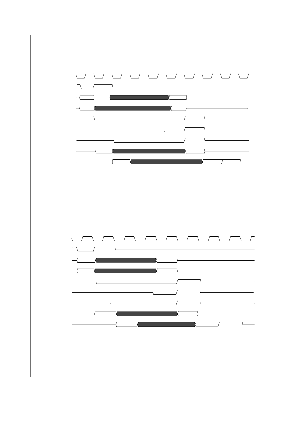
3.3.1 Target Read
A Target Read operation starts with the system generating
FRAMEN, Address, and either an IO read (0010b) or
Memory Read (0110b) command. See Figure 3-4. If the
32-bit address on the address bus matches the IO address
range specified in CFGIOA:IOBASE (for I /O reads) or the
memory address range specified in CFGMA:MEMBASE
(for memory reads), the DP83820 will generate DEVSELN
2 clock cycles later (medium speed).
The system must tri-state the Address bus, and convert the
C/BEN bus to byt e enables, after the address cycl e. On the
2nd cycle after the assertion of DEVSELN, all 32-bits of
data and TRDYN will become valid. If IRDYN is asserted at
that time, TRDYN will be forced HIGH on the next clock for
1 cycle, and then tri-stated.
Byte 3Byte 2Byte 1Byte 0
31 24 23 16 15 8 7 0
(MSB)
(LSB)
C/BEN[3] C/BEN[2] C/BEN[1] C/BEN[ 0]
Byte 0Byte 1Byte 2Byte 3
31 24 23 16 15 8 7 0
(LSB)
(MSB)
C/BEN[3] C/BEN[2] C/BEN[1] C/BEN[ 0]
3.0 Functional Description
(Continued)
11
www.national.com
If FRAMEN is asserted beyond the assertion of IRDYN, the
DP83820 will still make data available as descri bed above,
but will also issue a Disconnect. That is, it will assert the
STOPN signal with TRDYN. STOPN will remain as serted
until FRAMEN is detected as deass erted.
Figure 3-4 Target Read Operation
3.3.2 Target Writ e
A Target Write operation starts with the system generating
FRAMEN, Address, and Command (0011b or 0111b). See
Figure 3-5. If the upper 24 bi ts on the address bus match
CFGIOA:IOBASE (for I/O reads) or CFGMA:MEMBASE
(for memory reads), the DP83820 will generate DEVSELN
2 clock cycles later.
On the 2nd cycle after the assertion of DEVSELN, the
device will monitor the IRDYN signal. If IRDYN is asserted
at that time, the DP83810 will assert TRDYN. On the next
clock the 32-bit double word will be latched in, and TRDYN
will be forced HIGH for 1 cycle and then tri-stated.
Note: Target write operations must be 32-bits wide.
If FRAMEN is asserted beyond the assertion of IRDYN, the
DP83820 will still la tch the fi rst double word as descr ibed
above , but will also i ssue a Disconnect. That is, it will assert
the STOPN signal with TRDYN. STOPN will remain
asserted until FRAMEN is detected as deasserted.
Figure 3-5 Target Write Operation
Addr
Data
CLK
FRAMEN
AD[31:0]
C/BEN[3:0]
IRDYN
TRDYN
DEVSELN
PAR
PERRN
Addr Data
CLK
FRAMEN
AD[31:0]
C/BEN[3:0]
IRD YN
TRDYN
DEVSELN
PAR
PERRN

3.0 Functional Description
(Continued)
12
www.national.com
3.3.3 Master Read
A Master Read operation starts with the DP83820
asserting REQN. See Figure 3-6. If GNTN is asserted
within 2 clock cycles, FRAMEN, Address, and Command
will be generated 2 clocks after REQN (Address and
FRAMEN for 1 cycle only). If GNTN is asserted 3 cycles or
later, FRAM EN, Address, and Command will be generated
on the clock following GNTN.
The device will wait for 8 cycles for the assertion of
DEVSELN. After 8 clocks without DEVSELN, the device
will issue a Master Abort by asserting FRAM EN HIGH for 1
cycle. IRDYN will be forced HIGH on the following cycle.
Both signals will become tri-state on the cycle following
their deassertion.
On the clock edge after the generation of Address and
Command, the address bus will become tri-state, and the
C/BEN bus will contain valid byte enables. On the clock
edge after FRAMEN was asserted, IRDYN will be asserted
(and FR AMEN will be deasserted if this is to be a single
read operation). On the clock where both TRDYN and
DEVSELN are detected as as serted, data will be latched in
(and the byte enables will change if necessary). This will
continue until the cycle following the deassertion of
FRAMEN.
On the clock where the second to last read cycle occurs,
FRAMEN will be forced HIGH (it will be tri-stated 1 cycle
later). On the next clock edge that the device detects
TRDYN asser ted, it will force IRDYN HIGH. It, t oo, will be
tri-stated 1 cycle later. This will conclude the read
operation. The DP83820 will never f orce a wait state during
a read operation.
Figure 3-6 Master Read Operat ion
3.3.4 Master Writ e
A Master Write operation starts with the DP83820
asserting REQN. See Figure 3-7. If GNTN is asserted
within 2 clock cycles, FRAMEN, Address, and Command
will be generated 2 clocks after REQN (Address and
FRAMEN for 1 cycle only). If GNTN is asserted 3 cycles or
later, FRAM EN, Address, and Command will be generated
on the clock following GNTN.
The device will wait for 8 cycles for the assertion of
DEVSELN. After 8 clocks without DEVSELN, the device
will issue a Master Abort by asserting FRAM EN HIGH for 1
cycle. IRDYN will be forced HIGH on the following cycle.
Both signals will become tri-state on the cycle following
their deassertion.
On the clock edge after the generation of Address and
Command, the data bus will become valid, and the C/BEN
bus will contain valid byte enables. On the clock edge after
FRAMEN was asserted, IRDYN will be asserted (and
FRAMEN will be deasserted if this is to be a single read
operation). On the clock where both TRDYN and
DEVSELN are detected as asserted, valid data for the next
cycle will become available (and the byte enables will
change if necessary). This will continue until the cycle
following the deassertion of FRAMEN.
On the clock where the second to last write cycle occurs,
FRAMEN will be forced HIGH (it will be tri-stated 1 cycle
later). On the next clock edge that the device detects
TRDYN asser ted, it will force IRDYN HIGH. It, t oo, will be
tri-stated 1 cycle later. This will conclude the write
operation. The DP83820 will never f orce a wait state during
a write operati on.
Addr
Data
CLK
FRAMEN
AD[31:0]
C/BEN[3:0]
REQN
GNTN
IRD YN
TRDYN
DEVSELN
PAR
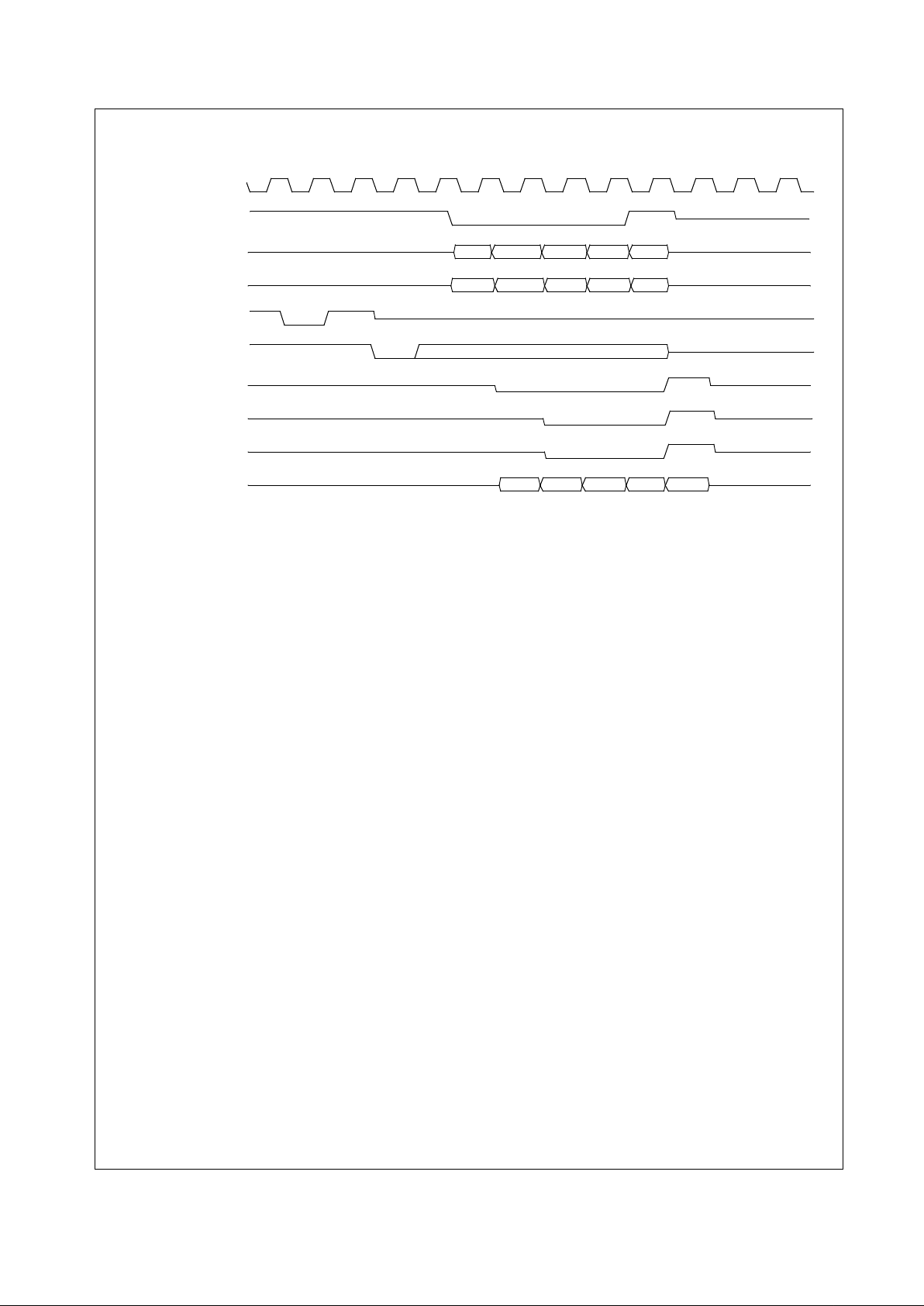
3.0 Functional Description
(Continued)
13
www.national.com
Figure 3-7 Master Write Operation
3.3.5 Configurati on Access
Configuration register accesses are similar to Target reads
and writes in that they are singl e data word transfer s and
are initiated by the system. For the system to initiate a
Configuration access, it must also generate IDSELN as
well as the correct Command (1010b or 1011b) during the
Address phase. The DP83820 will respond as it does
during Target operations.
Note: Configuration reads must be 32-bits wide, but writes may access individual
bytes.
3.4 Packet Buffering
The DP83820 incorporates two independent FIFOs for
transferring data to/from the system interface and from/to
the network. The FIFOs, providing temporary storage of
data, free the host system from the real-time demands of
the network.
The way in which the FIFOs are emptied and filled is
controlled by the FIFO threshold values in the TXCFG and
RXCFG registers (See Sections 4.2.12 and 4.2.16). These
values determine how full or empty the FIFOs must be
before the device requests the bus. Additionally, there is a
threshold value that determines how f ull the transmit FIFO
must be before beginning tr ansm ission. Once the DP83820
requests th e bus, it will attempt to empty or fill the FIFOs as
allowed by the respective MXDMA settings in TXCFG and
RXCFG.
3.4.1 Transmit Buf fer Manager
The buffer management scheme used on the DP83820
allows quick, simple and efficient use of the frame buffer
memory. The buffer management scheme uses separate
buffers and descriptors for packet infor mation. This allows
effective transfers of data to the transmit buffer manager by
simply transferring the descriptor information to the
transmit queue. Refer to the Buffer Management section for
complete information.
The Tx Buffer Manager DMAs packet data from PCI
memory space and places it in the 8KB transmit FI FO, and
pulls data from the FIFO to send to the Tx MAC. Multiple
packets may be present in the FIFO , allowing packets to be
transmitted with minimum int erframe gap. The way in which
the FIFO is emptied and filled is controlled by the FIFO
threshold values in the TXCFG register: FLTH (Tx Fill
Threshold), and DRTH (Tx Drain Threshold). Additionally,
once the DP83820 requests the bus, i t will attempt to fill the
FIFO as allowed by the MXDMA setting in the TXCFG
register.
3.4.2 Transmit Priority Queueing
The Tx Buffer Manager process also supports priority
queueing of transmit packets. It handles this by drawing
from four separ ate descriptor lists to fill the internal FIFO . If
packets are available in the higher priority queues, they will
be loaded into the FIFO before those of lower priority.
3.4.3 Receive Buffer Manager
The Rx Buffer Manager uses the sam e buffer management
scheme as used for transmits. Refer to the Buffer
Management section for complete information.
The Rx Buffer Manager retrieves packet data from the Rx
MAC and places it in the 32KB receiv e dat a FIFO , and pulls
data from the FIFO for DMA to PCI memory space. The Rx
Buffer Manager maintains a status FIFO, allowing up to 32
packets to reside in the FIFO at once. Similar to the
transmit FIFO, the receive FIFO is controlled by the FIFO
threshold value in RXCFG:DRTH (Rx Drain Threshold).
This value determines the number of long words wr itten
into the FIFO from the MAC unit before a DMA request for
system memory occurs. Once the DP83820 gets the bus, it
will continue to transfer the long words from the FIFO until
the data in the FIFO is less than one long word, or has
reached the end of the packet, or the max DMA burst size
is reached (RXCFG register:MXDMA).
3.4.4 Receive Priorit y Que ueing
The Rx Buffer Manager process also supports priority
queueing of receive packets. It handles this by placing
packets on up to four separate descriptor lists when
emptying the inter nal FIFO. The Rx Buffer Manager uses
information in a VLAN tag to determine packet priority.
Addr
Data
CLK
FRAMEN
AD[31:0]
C/BEN[3:0]
REQN
GNTN
IRD YN
TRDYN
DEVSELN
PAR

3.0 Functional Description
(Continued)
14
www.national.com
3.4.5 Packet Recognition
The Receive packet filter and recognition logic allows
software to control which packets are accepted based on
destination address and packet type. Address recognition
logic includes suppor t for broadcast, multicast hash, and
unicast addresses. The packet recognition logic includes
support for WOL, Pause, and programmable pattern
recognition.
3.5 Ethernet Media Access Controller (MAC)
The Media Access Control (MAC) unit perform s the control
functions for the media ac cess of transmitting and receiving
packets. During transmission, the MAC unit handles
building of frames and tr ansmission of the frames over the
interface to the physical layer device. During reception,
data is received from the physical layer interface, the frame
is checked for v alid reception, and the data is trans ferred to
the receive FIFO. Control and status registers in the
DP83820 gover n the operation of the MAC unit.
The standard 802.3 Ethernet packet consists of the
following fields: preamble, start of frame delimiter (SFD),
destination address, source address, length, data, frame
check sequence (FCS) and Extension (See Fi gure 3-8). All
fields are of fixed length except for the data field and
Extension. The Extension field is only used for 1000 Mb/s
half-duplex operation. During recepti on, the preamble and
SFD are stripped from the incoming packet. During
transmission, the DP83820 generates and prepends the
preamble and SFD. The FCS is normally appended by the
DP83820, but software may disable FCS inclusion on a
per-packet basis.
Figure 3-8 IEEE 802.3 Packet Structur e
3.5.1 Full Duplex Operation
Full duplex operation i s the simultaneous transmission and
reception of packet data. In t his mode of operation, r eceive
activity (CRS) is ignored in the decision making process for
transmissi on. During reception, collisions are al so ignored.
To configure the DP83820 to operate in full duplex, set
TXCFG:CSI
and
TXCFG:HBI=1
, and
RXCFG:RX_FD
= 1.
3.5.2 Full Duplex Flow Control
The DP83820 supports full duplex flow control using the
MAC Control Pause Frame as defined in the 802.3
specification. The packet recognition logic can detect
Pause frames, and cause the transmit MAC to pause the
correct number of slot times. In addition, the MAC can be
programmed to send Pause frames based on Rx FIFO
thresholds.
Flow Control operation is controlled by the Pause
Control/Stat us Register .
3.5.3 1000 Mb/s Operati on
The DP83820 includes additional features to support 1000
Mb/s speed of operation. In this mode, the physical layer
interface is increased from 4-bit MII to 8-bit GMII (or 10-bit
TBI). In addition, features such as carrier extension and
frame burst ing are required to meet the 802.3 specification
for 1000 Mb/s half-duplex operation.
3.6 Transmit MAC
The Transmit MAC implements the transmit portion of
802.3 Media Access Control. The Tx MAC retrieves packet
data from the Tx Buffer Manager and sends it out through
the transmit physical layer interface. Additionally, the Tx
MAC provides MIB control information for transmit packets.
The TX MAC supports 4-bit MII, 8-bit GMII, and 10-bit TBI
interf aces to physical layer devices
3.6.1 VLAN Tag Insertion
The Tx MAC has the capability to insert a 4-byte VLAN tag
in the transmit packet. If Tx VLAN Tag insertion is enabled,
the MAC will insert the 4 bytes, as specified in the VTAG
register, following the source and destination addresses of
the packet. The VLAN tag insertion can be enabled on a
global or per-packet basis.
3.6.2 Carrier Extension
For 1000 Mb/s half-duplex operation it is necessary for
MAC to ensure that all valid carrier events exceed a
slotTime of 4096 bit ti me s. To accomplish this, any transmit
event that is shorter than the slotTime will be extended
using Carrier Extension. On the GMII interface, this is
signaled to the Phy by TXER asserted with TXEN
deasserted and a TXD value of 0x0F.
3.6.3 Frame Bursting
The Tx MAC supports burst mode operation for 1000 Mb/s
half-duplex operation. This allows the device to transmit a
burst of packets without releasing control of the physical
medium. After a successful transmission, if additional
packets are available, the MAC will transmit a burst of
packets wi thout allowing the medium to go idle. It does thi s
by inserting carrier extension between the frames. The
MAC will continue to burst frames as long as additional
packets are available in the internal FIFO and a burstLimit
of 65536 bit times has not been exceeded.
3.6.4 IP Checksum Generation
The Tx MAC supports task offloading of IP, TCP, and UDP
checksum generation. It can generate the checksums and
insert them into the packet. The checksum generation can
be enabled on a global or per- packet basis.
3.7 Receive MAC
This block implements the receive portion of 802.3 Media
Access Control. The Rx MAC retrieves packet data from
the receive portion and sends it to the Rx Buffer Manager.
Additionally, the Rx MAC provides MIB control information
and packet address data for the Rx Filter. The RX MAC
supports 4-bit MII, 8-bit GMII, and 10-bit TBI interfaces to
physical layer devices.
preambl e S FD dest ad dr src addr le n
data
fcs
7 bytes 1 byte 6 bytes 6 bytes 2 bytes
46 to 1500 bytes 4 byte s
extension
<512 bytes

3.0 Functional Description
(Continued)
15
www.national.com
3.7.1 VLAN Tag Handling
The Rx MAC can detect packets containing a 4-byte VLAN
tag, and remove the VLAN tag from the received packet. If
RX VLAN Tag removal is enabled, then the 4 bytes
following the source and destination addresses will be
stripped out. The VLAN status can be returned in the
Receive Descriptor Extended Status field.
3.7.2 Carrier Extension and Packet Bursting
The Receive MAC supports reception of packets with
Carrier Extension and packets transmitted using Frame
Bursting for 1000 Mb/s half-duplex operation. The first
frame in a burs t must be at least one slotTime in length,
otherwise it will be considered to be a collision fragment.
3.7.3 IP Checksum Verification
The Rx MAC supports IP checksum verification. It can
validate IP checksums as well as TCP and UDP
checksums. Packets can be discarded based on detecting
checksum errors.
3.8 P hysical L ayer Interface
The DP83820 implements a physical layer interface that
can support all of the following:
— Media Independent Interface (MII)
— Gigabit Media Independent Interface (GMII)
— Ten-Bit Interface (TBI)
In addition, the DP83820 implements a Management
interf ace as defined for MII and GMII.
3.8.1 Media Independ ent Interface (MII)
The DP83820 supports 10 Mb/s and 100 Mb/s physical
layer devices through the Media Independent Interface
(MII) as defined in IEEE 802.3 (clause 22). The MII
consists of a transmit data interface (TXEN, TXER,
TXD[3:0], and TXCLK), a receive data interface (RXDV,
RXER, RXD[3:0], and RXCLK), 2 status signals (CRS and
COL) and a management inter face (MDC and MDIO). In
this mode of operation, both Transmit and Receive clocks
are supplied by the Phy.
3.8.2 Gigabit Media Independ ent I nterface (GMII)
The DP83820 can support 1000 Mb/s physical layer
devices thr ough the Gigabit Media Independent Interface
(GMII) as defined in I EEE 802.3 (cl ause 35). The GMII is
extended from the MII to use 8-bit data interfaces and to
operate at higher frequency. The GMII consists of a
transmit data interface (TXEN, TXER, TXD[7:0], and
GTXCLK), a receive data interface (RXDV, RXER,
RXD[7:0], and RXCLK), 2 status signals (CRS and COL)
and a management interface (MDC and MDIO). Many of
the signals are shared with the MII interface. One
significant difference is the Transmit clock (GTXCLK) is
supplied by the DP83820 instead of the Phy. The
management interface (described later) is the same in both
MII and GMII modes
3.8.3 Ten-Bit Interface (TBI)
The TBI provides a port for transmit and receive data for
interfacing to devices that support the 1000Base-X portion
of the 802.3 specifi cation. This includes 1000Base-FX fiber
devices. The por t consists of data paths that are 10-bits
wide in each direction as well as control signals. This
interface shares pins with the MII and GMII interfaces.
3.8.4 MII/GMII Management Interface
The MII/GMII management interface utilizes a
communication protocol similar to a serial EEPROM.
Signaling occurs on two signals: clock (MDC) and data
(MDIO). This protocol provides capability for addressing up
to 32 individual Physical Media Dependent (PMD) devices
which share the same serial interface, and for addressing
up to 32 16-bit read/wr ite registers within each PMD. The
MII management protocol utilizes following frame format:
start bits (SB), opcode (OP), PMD address (PA), register
address (RA), line turnaround (LT) and data (See Figure 3-
9).
Figure 3-9 MII Management Frame Format
— Start bits are define d as <01>.
— Opcode bits are defined as <01> for a Write access and
<10> for a Read access.
— PMD address is the device addr ess.
— Register address is address of the register within that
device.
— Line turnaround bits wil l be <10> for Write acces ses and
will be <xx> for Read accesses. This allows time for the
MII lines to “turn around”.
— Data is the 16 bits of data that will be written to or read
from the PMD device.
A reset frame is also provided and defined as 32
consecutive 1s (FFFF FFFFh). After power up, all MII PMD
devices must wait for a reset frame to be received prior to
participating in MII management communication.
Additionally, a reset frame may be issued at any time to
allow all connected PMDs to re-synchronize to the data
traffic.
The MII/EEPROM Access Register (MEAR) is used to
provide access to the serial MII.
Refer to Section 4. 2.3 for compl ete details of the MEAR.
2b
2b 5b 5b 2b 16b
SB OP
PA RA
LT
Data
Note: b = bits

3.0 Functional Description
(Continued)
16
www.national.com
3.9 EEPROM Inte rface
The DP83820 supports the attachment of an external
EEPROM. The EEPROM int erface provides the ability for
the DP83820 to read from and write data to an external
serial EEPROM device. Values in the external EEPROM
allow default fields in PCI configuration space and I/O
space to be overridden following a hardware reset. The
DP83820 will "autoload" v alues from the EEPROM to these
fields in configuration space and I/O space and perform a
checksum to verify that the data is valid. If the EEPROM is
not present, the DP83820 initialization uses default values
for the appropriate Configuration and Operational
Registers. Software can read and write to the EEPROM
using “bit-bang” accesses via the MII/EEPROM Access
Register (MEAR).
3.10 Boot ROM Interface
The BIOS ROM interface allows the DP83820 to read from
and writ e d at a to an external PROM /F la s h device.
3.11 Power Managemen t and Wake Functions
The DP83820 is compliant with the PCI Power
Management Specification v1.1. The device can be
programmed to any of the powered states (D0, D1, D2,
D3hot) and enabled to assert its PMEN pin through the
Configuration Register PMCSR. In addition, the device will
enter the D3cold state when PCI power is dropped,
regardless of the programmed power state. In either D3hot
or D3cold, if PMEN assertion is enabled, the device will
keep the receiver alive so that it may recognize wake
packets and signal the system to wake up; if PMEN
assertion is not enabl ed, the device will go to sleep and be
unable to rec eive packets.
The DP83820 supports several types of wake events that
will signal the power management logic to assert PMEN.
These are detailed in the Wake On LAN section (4.2.18.1).
In order for the device to request a system wake, at least
one wake e vent must be configured in the Wake Command
and Status Register (WCSR). If PMEN assertion i s enabled
and the device enters the D3cold state with no wake events
enabled, the device will go to sleep.
When the device is in a power management state other
than D0 (the fully alive state), the only PCI bus activity it
may initiate is the assertion of PMEN. This means any
packets received will remain in the receive FIFO until the
device is returned to the fully alive state. Upon waking up,
the wake packet is availab le i n the receive FIFO.
In any power state, enabling PMEN assertion adds
additional packet filtering: only those packet types that are
configured as wake packets in WCSR will be accepted.
This prevents non-wake packets from filling the receive
FIFO while the device is in a low power state and
preventing a wake packet from being accepted. It is
expected that while in the fully alive state, PMEN assertion
will be disabled to eliminate the extra level of filtering.
3.12 Network Management Fu nct i ons
The DP83820 allows compliance with several layer
management standards to allow a node to monitor overall
network perf ormance. These standards are:
— RFC 1213 (MIB II),
— RFC 1643 (Ether-like MIB), and
— IEEE 802.2 Layer Management.
Many of the counters required by these standards are
easily maintained in software during normal per-packet
processing. Those counters that would either be difficult or
impossible for software to maintain are provided for in
hardware (See Section 4.2.27). The table below outlines
each required counter, the relevant standard, and how the
counter should be maintained.
Table 3-1 MIB Compliance
Counter Name Reference Maintained by Derivation
RXOctetsOK RFC 1213,
802.3 LM
softw are, ad d cmdsts .SIZE on
receive packets with
cmdsts.OK bit set.
The byte count of each successfully
received packet is added to this counter.
The pac ket byte co un t in cl ud es the ad dres s ,
type, data, and FCS fields.
RXFramesOK 802.3 LM software, increment on
receive packets with
cmdsts.OK bit set.
This coun t er is in cr em ente d for each pack et
successfully received (this includes
broadcast, multicast, and physical address
packets).
RXBroadcastPkts RFC 1213,
802.3 LM
software, increment on
receive packets with
cmdsts.OK set and
cmdsts.DEST set to 11.
This counter is incremented for each
broadcast packet successfully received.
RXMulticastPkts RFC 1213,
802.3 LM
software, increment on
receive packets with
cmdsts.OK set and
cmdsts.DEST set to 10.
This counter is incremented for each
multicast packet successfully received.
RXErroredPkts RFC 1213 hardware, see
MIB:RxErroredPkts.
This coun t er is in cr em ente d for each pack et
received with errors. This count includes
packets which are automatically rejected
from the FIFO due to both wire errors and
FIFO overruns.

3.0 Functional Description
(Continued)
17
www.national.com
RXFCSErrors RFC 1643,
802.3 LM
hardware, see
MIB:RXFCSErrors.
This coun t er is in cr em ente d for each pack et
received wit h a Frame Check Seque nc e
error (bad CRC).
RXMsdPktErrors RF C 1213, RFC
1643, 802.3 LM
hardware, see
MIB:RXMsdPktErrors.
This counter is incremented for each
receive aborted due to data or status FIFO
overruns (insuff icient buffer space).
RXFAEErrors RFC 1643,
802.3 LM
hardware, see
MIB:RXFAEErrors.
This coun t er is in cr em ente d for each pack et
received with a Frame Alignment error.
RXSymbolErrors 802.3 LM hardware, see
MIB:RXSymbolErrors
This coun t er is in cr em ente d for each pack et
received with one or more 100 Mb symbol
errors detected.
RXFrameTooLong RFC 1643,
802.3 LM
hardware, see
MIB:RXFrameTooLong.
This coun t er is in cr em ente d for each pack et
received with greater than the 802.3
standard maximum length of 1518 bytes.
RXIRLErrors 802.3 LM hardware, see
MIB:RXIRLErrors.
Packets received with In Range Length
errors. This counter increments fo r packets
received with a MAC length/type value
between 64 and 1518 bytes, inclusive, that
does no t match the number of bytes
received. This counter also increments for
packets with a MAC length/type field of less
than 64 bytes and more than 64 bytes
received.
RXBadOpcodes 802.3 LM hardware, see
MIB:RXBadOpcodes.
Packets received with a valid MAC control
type and an opcode for a function that is not
supported by the device
RXPauseFrames 802.3 LM hardware, see
MIB:RXPauseFrames.
MAC co ntrol Pause frames received.
TXOctetsOK RFC 1213,
802.3 LM
software, add sum of
cmdsts.SIZE (+4) on transmit
packets with cmdsts.OK bit
set.
The byte count of each successfully
transmitte d packet is added to thi s coun te r.
The pac ket byte co un t in cl ud es the ad dres s ,
type, data, and FCS fields.
TXFramesOK 802.3 LM software, increment on
transmit packets with
cmdsts.OK bit set.
This coun t er is in cr em ente d for each pack et
succe ss fu lly transm it t e d. T hi s co un t
includes broadcast, multicast, and physical
addres s packets.
TXDeferred RFC 1643,
802.3 LM
software, increment on
transmit packets with
cmdst s. TD se t .
This coun t er is in cr em ente d for each pack et
trans mis si on whic h i s de ferred due to a ctive
line conditions (once per packet).
TXBroadcastPkts RFC 1213,
802.3 LM
software, increment on
transmit packets with
cmdsts.OK set, and
destination address set to ffff-ff-ff-ff-ff
This counter is incremented for each
broadcast packet successfully transmitted.
TXMulticastPkts RFC 1213,
802.3 LM
software, increment on
transmit packets with
cmdsts.OK set, and LSB of
first byte of destination
addres s set.
This counter is incremented for each
multicast packet successfully transmitted.
TXFrames1Coll RFC 1643,
802.3 LM
software, increment on
transmit packets with
cmdsts.CCNT == 1 and
cmdsts.OK set.
This coun t er is in cr em ente d for each pack et
successfully transmitted with 1 in-window
collision.
TXFramesMultiColl RFC 1643,
802.3 LM
software, increment on
transmit packets with
cmdsts.CCNT > 1 and
cmdsts.OK set.
This coun t er is in cr em ente d for each pack et
successfully transmitted with 2-15 inwindow collisions.
TXPauseFrames 802.3 LM hardware, see
MIB:TXPauseFrames.
MAC co ntrol Pause frames transmitted.

3.0 Functional Description
(Continued)
18
www.national.com
3.13 Buffer Management
The buffer management scheme used on the DP83820
allows quick, simple and efficient use of the frame buffer
memory. Frames are saved in similar formats for both
transmit and receive. The buffer management scheme also
uses separate buffers and descriptors for packet
information. This allows effective t ransfers of data from the
receive buffer to the transmit buffer by simply transferring
the descriptor from the receive queue to the transmit
queue.
The format of the descriptors allows the packets to be
saved in a number of configurations. A packet can be
stored in memory with a single descriptor and a single
packet fragment, or multiple descriptors with single
fragments. This flexibility allows the user to configure the
DP83820 to maximize efficiency. Architecture of the
specific system’s buffer memory, as well as the nature of
network traffic, will determine the most suitable
configuration of packet descriptors and fragments.
3.13.1 Overview
The buffer management design has the follow ing goals:
— simplicity
— efficient use of the PCI bus (the overhead of the buffer
management technique is minimal),
— low CPU utilization,
— flexibility.
Descriptors may be either per-packet or per-packetfragment. Each descriptor may describe one packet
fragment. Receive and transmit descriptors are
symmetrical.
3.13.2 Descript or Format
DP83820 uses a symmetrical format for transmit and
receive descr iptors. In br idging and switching applications
this sym m e try allows so f tware to forward packets by simp l y
moving the list of descriptors that describe a single
received packet from the receive list of one MAC to the
transmit list of another. Descriptors must be aligned on a
64-bit boundary.
TXPktsErrored RFC 1213 software, increment on
receive packets with
cmdsts.TXA set
This coun t er is in cr em ente d for each pack et
encountering errors during transmissi on.
This count does include t ransmissions
abor ted manuall y and due to FIFO
underruns, but does not include packets
which experience less than 16 in-window
collisions.
TXExcessiveCollisions RFC 1643,
802.3 LM
software, increment on
transmit packets with
cmdst s. EC se t .
This counter is incremented for each
transmission aborted af ter experiencing 16
in-window co ll is ions.
TXExcessiveDeferral 802.3 LM software, increment on
transmit packets with
cmdst s. ED se t .
This counter is incremented for each
transmission aborted due to a time-out of
the excessive deferral timer (3.2ms).
TXOWC RFC 1643,
802.3 LM
software, increment on
transmit packets with
cmdst s. OWC se t .
This counter is incremented for each
transmission which is aborted due to an
out-of-window collision.
TXCSErrors RFC 1643,
802.3 LM
software, increment on
transmit packets with
cmdst s. CR S se t .
This counter is incremented for each
transmission on which carrier is not
detected after the start of transmission, or
carrier sense is lost during tr ansmission.
TXSQEErrors RFC 1643 hardware, see
MIB:TxSQEErrors
This counter is incremented when the
collision heartbeat pulse is not detected
from by the PMD after a transmission.

3.0 Functional Description
(Continued)
19
www.national.com
Table 3-2 DP83820 Descriptor Format
If 64-bit addressing is enabled, the link and bufptr fields are
64-bit fields. Otherwise, they are 32-bit fields. The
DP83820 supports an optional extended status field which
supports VLAN and IP functions. To enable the extsts field,
software should set the EXTSTS_EN bit in the CFG
register.
Some of the bit definitions in the
cmdsts
field are common
to both receive and transmit descriptors:
Table 3-3
cmdsts
Common Bit Definitions
Table 3-4 Tra nsmit
cmdsts
Bit De fin i tions
offset tag description
0000h link 32- or 64-bit "link" field to the next descriptor in the linked list. Bits 2-0 must be 0, as
descriptors must be aligned on 64-bit boundaries.
0004h or
0008h
bufptr 32- or 64-bit pointer to the first fragment or buffer. In transmit descriptors, the buffer can
begin on any byte boundary. In receive descriptors, the buffer must be aligned on a 64-bit
boundary.
0008h or
0010h
cmdsts 32-bit Command/Stat us Field (bit-encoded)
000ch or
0014h
extsts OPTIONAL 32-bit Extended Status Field. Contains VLAN and IP information.
bit tag description usage
31 OWN Descrip tor O w ne rsh i p Set to 1 by the data producer of the descriptor to transfer
owner s hi p to t h e da ta consumer of the descriptor. Set to 0 by
the data consumer of the descriptor to return ownership to
the data producer of the descriptor. For transmit descriptors,
the driver is the data producer, and the DP83820 is the data
consumer. For receive descriptors, the D P83820 is the data
producer, and the driver is the data consumer.
30 MORE More descriptors Set to 1 to indicate that this is NOT the last descriptor in a
packet (there are MORE to follow). When 0, this descriptor is
the last descriptor in a packet. Completion status bits are
only valid whe n t hi s bi t is zero.
29 INTR Interrupt Set to 1 by software to request a "descriptor interrupt" when
DP838 20 transfers the ownership of this descriptor back to
software.
28 SUPCRC
INCCRC
Suppress CRC / Include
CRC
In tr an smit d es cript o rs, t his indi ca t es th at CRC s ho uld no t be
appended by the MAC. On receives, this bit will be set based
on the RXCFG:INCCRC bit.
27 OK Packet OK In the last descriptor in a packet, this bit indicates that the
pac ket was either se nt or received successfully.
26-16 --- The usage of these bits differ in receive and transmit
descriptors. See below for details.
15-0 SIZE Descriptor Byte Count Set to the size in bytes of the data.
bit tag description usage
26 TXA Transmit Abort Transmission of this packet was aborted.
25 TFU Transmit FIFO Underrun The transmi t FIFO wa s e x ha uste d du ring the tr ans mi ssi on of
this packet.
24 CRS Carrier Sen s e Los t Carrier was lost during the transmission of this packet. This
condition is not reported if TXCFG:CSI is set.
23 TD Transmit Deferred Transmission of this packet was deferred.
22 ED Excessive D eferral The length of deferral during the transmission of this packet
was excessive.
21 OWC Out of Window Collision The MAC encountered an "out of window " collision during
the transmission of this packet.

3.0 Functional Description
(Continued)
20
www.national.com
Table 3-5 Receive
cmdsts
Bit Definitions
20 EC Excessive Collisions The number of collisi ons during the transmission of this
packet was excessive, indicating transmission failure.
If TXCFG register ECRETRY=0, this bit is set after 16
collisions.
If TXCFG register ECRETRY=1, this bit is set after 4
Excessive Collision events (64 collisions).
19-16 CCNT Collision Count If TXCFG register ECRETRY=0, this field indicates the
numb er of collisions e ncountered during the transmission of
this packet.
If TXCFG register ECRETRY=1,
CCNT[3:2] = Excessive Collisions (0-3)
CCNT[1] = Multiple Collisions
CCNT[0] = Single Collision
Note that Excessive Collisions indicate 16 attempts failed,
while Multiple Col li si on s an d S in gle Co ll is io n ind ic ate
collisions in addition to any excessive collisions. For
example, a collision count of 33 includes 2 Excessive
Collisions and will also set the Single Collision bit.
bit tag description usage
26 RXA Receive Aborted Set to 1 by DP83820 when the receive was aborted. If RXO
is set, then the receive was aborted due to an RX overrun. If
RXO is clear, then a receive descriptor error occurred. SIZE
will be set to the amount of data that was transferred to
memory when the error was detected.
25 RXO Receive Overr un Set to 1 by DP83820 to indicate that a receive overrun
condi tion occurred. RXA will also be set.
24-23 DEST Destination Class When the receive filter is enabled, these bits will indicate the
destination address class as follows:
00 - Packet was rejected
01 - Destination matched the Receive Filter Node Address
Register
10 - Destination is a multicast (but not broadcast)
11 - Destination is a broadcast address
If the R eceive Filter is enabled, 00 indicates that the packet
was rejec ted . N ormally packets that are rejecte d do not
cause any bus activity, nor do they consume receive
descriptors. However, this condition could occur if the packet
is rejected by the Receive Filter later in the packet than the
receive drain threshold (RXCFG:DRTH)
22 LONG Too Long Packet
Received
The size of the receive packet exceeded 1518 bytes (1522
bytes if VLAN tag included ).
21 RUNT R u nt Packet Rec e ived The size of the receive packet was smaller than 64 bytes
(including CRC).
20 ISE Invalid Symbol Error (100 Mb only) An invalid symbol wa s enc ount er ed du ri ng the
reception of this packet.
19 CRCE CRC Error The CRC appended to the end of thi s packet was invalid.
18 FAE Frame Alignment Er ror Th e packet did not contain an integral number of octets.
17 LBP Loopback Packet The packet is the result of a loopback transmission.
16 IRL In-Ran ge Length Error The receive packet Length/Type field did not match the
length of the data field for the packet. Only valid if the
Length/Type field is a valid length (not a Type value).

3.0 Functional Description
(Continued)
21
www.national.com
Table 3-6 Transmit
extsts
Bit De fin i tions
T able 3-7 Receive
extsts
Bit Defi n itions
bit tag description usage
31-22 unused
21 UDPPKT UDP Packet Indicates packet contains a UDP header and enables
checksum generation for the UDP header if Checksumming
is ena bled on a per-pa cket basis .
20 unused
19 TCPPKT TCP Packet Indicate s packet contains a TCP header an d enables
checksum generation for the TCP header if Checksumming
is ena bled on a per-pa cket basis .
18 unused
17 IPPKT IP Packet Indicates packet contains a IP header and enables
checksum generation for the IP header if Checksumming is
enabled on a per- pa cket basis.
16 VPKT VLAN Packet Inser t VLAN tag.
15-0 VTCI VLAN Tag Control
Information
This is the VLAN TCI field to be inserted in the packet if the
VPKT bit is set.
bit tag description usage
31-23 unused
22 UDPERR UDP Checksum Error Indicates a checksum error was detected in the UDP header.
21 UDPPKT UDP Packet Indicates an UDP header was detecte d for the packet.
20 TCPERR TCP Checksum Error Indicates a checksum error was detected in the TCP header.
19 TCPPKT TCP Packet Indicate s an TCP header was detected for the pack et.
18 IPERR IP Checksum Error Indicates a checksum error was detected in the IP header.
17 IPPKT IP Packet Indicates an IP header was detected for the packet.
16 VPKT VLAN Packet Packet contained a VLAN tag. This bit will be set if VLAN
packet detectio n is enabled and the packet contained the
correct ty pe value.
15-0 VTCI VLAN Tag Control
Information
This is the VLAN TCI field to be extracted from the packet. It
contain s the us er _ prior ity, CFI, and VID fi e lds .
3.0 Functional Description
(Continued)
22
www.national.com
3.13.2.1 Single Descriptor Packets
To represent a packet in a single descript or, the MORE bit in the
cmdsts
field is set to 0.
Figure 3-10 Single Descripto r Packets
3.13.2.2 Mult ipl e Descriptor Packets
A single packet may also cross descriptor boundaries. This
is indicated by setting the MORE bit in all descriptors
except the last one in the packet. Ethernet inter-networking
applications (bridges, switches, router s, etc.) can optimize
memory utilization by using a single small buffer per
receive descr iptor, and allowing the DP83820 hardware to
use the minimum number of buffers necessary to store an
incoming packet.
Figure 3-11 Multiple Descriptor Packets
3.13.2.3 Descriptor Rings
The simplest and recommended organization of
descriptors is in a fixed ring implementation. At
initialization, the driver can set up a fixed list of descriptors
complete with links connecting the descriptors in a ring. All
descriptors will initially be owned by the producer of the
data (the driver for transmit, the DP83820 for receive). The
OWN bit is used by both driver and the DP83820 to
indicate data availability and to release descriptors back to
the producer. When using a descriptor ring, the driver
should never need to modify any fields of a descriptor it
does not own. For transmit, the driver should never assign
all descriptors to the device, reserving one descriptor to
terminate the list, preventing the device from wrapping
completely around the ring.
link
bufptr
MAC hdr
netwk hdr
data
0
64
single descriptor / single fragment
link
bufptr
MAC hdr
netwk hdr
data
1
14
multiple descriptor / single fragment
link
bufptr
1
20
link
bufptr
0
30
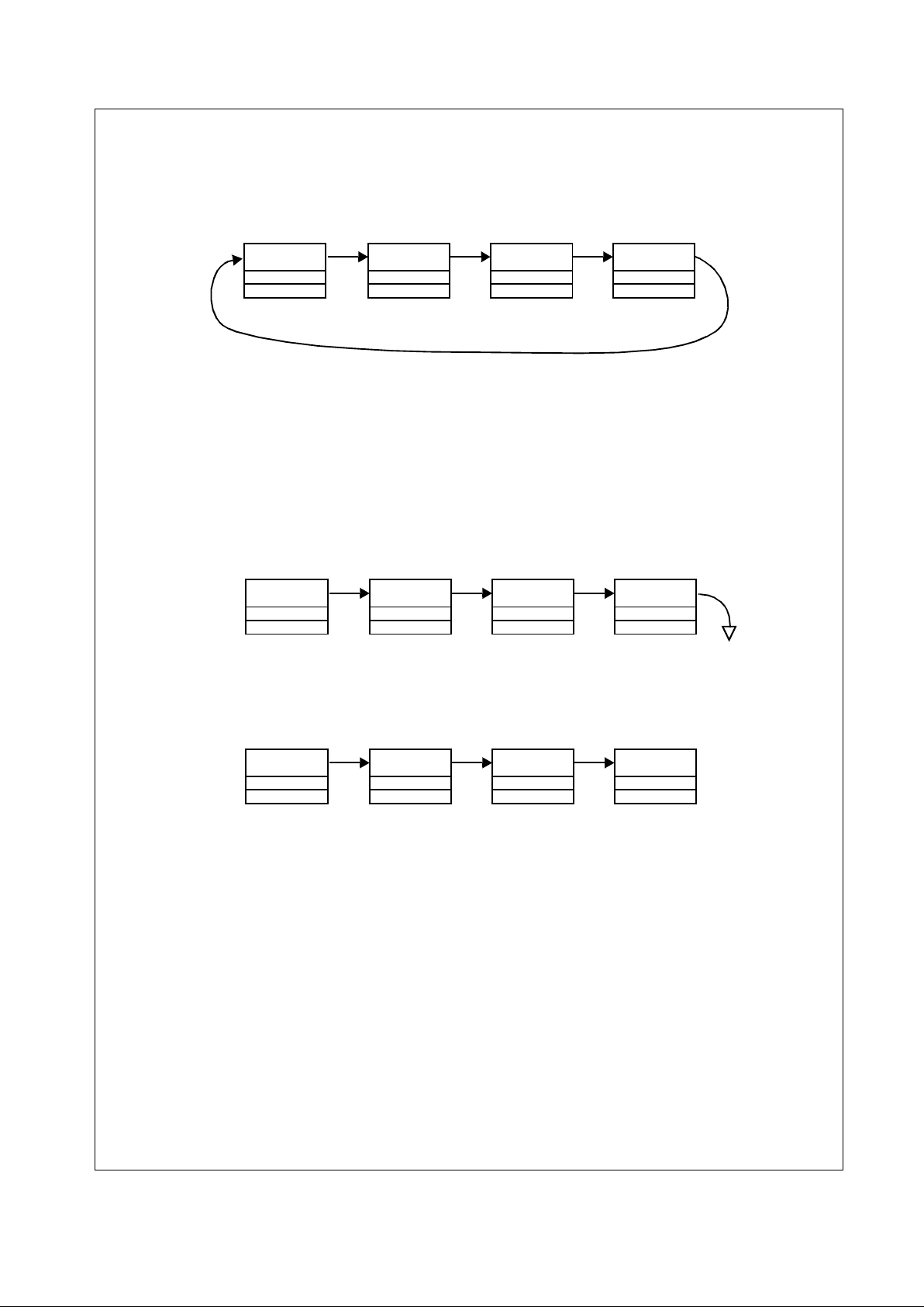
3.0 Functional Description
(Continued)
23
www.national.com
Figure 3-12 Ring Descriptor Organization
3.13.2.4 Descriptor Lists
Descriptors may also be organized in linked lists using the
link field. The linked list may be terminated by either a
NULL link field, or by using the descriptor OWN bit. A list of
descriptors ma y repres ent any num ber of pac k ets or pac ke t
fragments. Care should be used when implementing a
linked list terminated by a NULL link as there is a potential
for driver software and the device to get out of sync. Before
clearing a link field when freeing up descriptors, the driver
should verif y that the device has al ready traversed the li nk.
Figure 3-13 Linked List Descr iptor Organization
10180
addr 10140
10140
addr 10100
101C0
addr 10180
10100
addr 101C0
Descriptors Organized in a Ring (Recommended Method)
10180
addr 10140
10140
addr 10100
101C0
addr 10180
addr 101C0
Linked List terminated by OWN bit
10180
addr 10140
10140
addr 10100
101C0
addr 10180
00000
addr 101C0
Linked List terminated by NULL li nk field
own !own
ownown
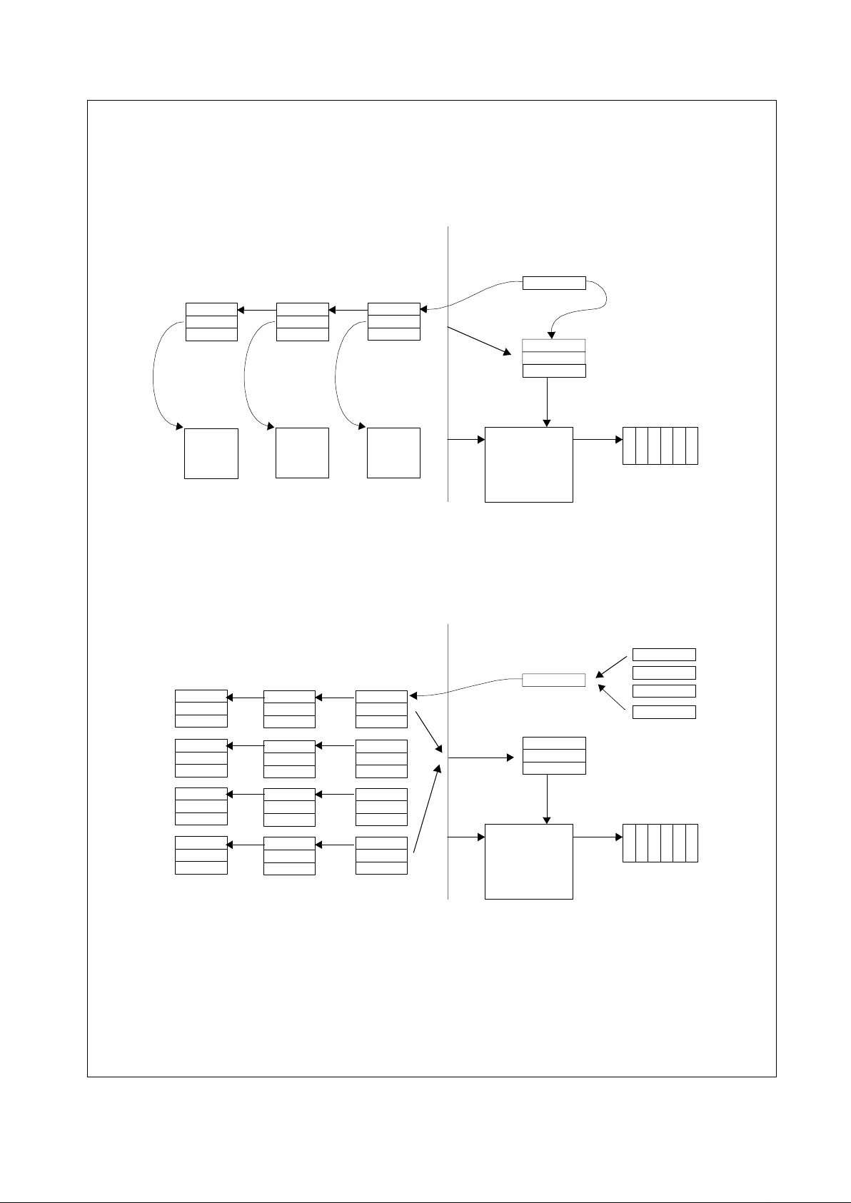
3.0 Functional Description
(Continued)
24
www.national.com
3.13.3 Transmit Architecture
The Transmit architecture can support a single transmit
queue, or can support multiple transmit queues for
handling priority traf fic. The following figures illustrate t he
transmit architecture of the DP83820 10/100 Ethernet
Controller with and without Priority Queueing.
Figure 3-14 Transmit Architecture without Priority Queueing
Without Priority Queueing, the device will draw packets
from a single Descriptor list. Only one descriptor pointer is
required. When the CR:TXEN bit is set to 1 (regardless of
the current state), and the DP83820 tr ansmitter is idle, t hen
DP83820 will read the contents of the current transmit
descriptor into the TxDescCache. The DP83820’s
TxDescCache can hold a single fragment pointer/count
combination.
Figure 3-15 Transmit Architecture with Prior ity Queueing
With Priority Queueing, the device will draw packets from
up to 4 Descriptor lists. The device has four descriptor
pointers and associated control logic to keep track of when
descriptors are available with valid packet information. In
this case, pulsing CR:TXEN with CR:TXPRI[p] set will
indicate to the DP83820 that a descriptor is available for
descriptor queue of priority ‘p’. Based on the priority
algorithm in use, the device will draw from the current
highest priority descriptor that has packets available for
transmission. There is no reordering of packets once they
are queued within the internal FIFO.
Transmit Descr iptor
Current Tx Desc Ptr
Software/Memory Hardware
Tx Data FIFO
link
bufptr
cmdsts
cmdsts
Tx DMA
bufptr
Packet
TxHead
link
Tx Desc Cache
link
bufptr
cmdsts
Packet
link
bufptr
cmdsts
Packet
Transmit Descr iptor
Current Tx Desc Ptr
Software/Memory Hardware
Tx Data FIFO
link
bufptr
cmdsts
cmdsts
Tx DMA
bufptr
TxHead
link
Tx Desc Cache
link
bufptr
cmdsts
link
bufptr
cmdsts
link
bufptr
cmdsts
link
bufptr
cmdsts
link
bufptr
cmdsts
link
bufptr
cmdsts
link
bufptr
cmdsts
link
bufptr
cmdsts
link
bufptr
cmdsts
link
bufptr
cmdsts
link
bufptr
cmdsts
TXDP1
TXDP2
TXDP3
TXDP4
Q0
Q1
Q2
Q3

3.0 Functional Description
(Continued)
25
www.national.com
3.13.3.1 Trans mit Sta te Machine
The transm it state machine has the following states:
The transm it state machine manipulates the following i nternal data spaces:
Inputs to the transmit state machine include the following events:
T able 3-8 Transmit State Tables
txIdle The transmit state machine is idle.
txDescRefr Wait ing for the "r efresh" transfer of the link field of a completed descri ptor from the PCI bus.
txDescRead Waiting for the transfer of a complete descriptor from the PCI bus into the
TxDescriptorCache.
txFifoBlock Waiting for free space in the TxDataFIFO to reach TxFillThreshold.
txFragRead Waiting for the transfer of a fragment (or portion of a fragment) from the PCI bus to the
TxDataFIFO.
txDescWrite Waiting for the completion of the write of the
cmdsts
field of an intermediate transmit
descriptor (cmdsts.MORE == 1) to host memory .
txAdvance (transitory state) Examine the link field of the current descriptor and advance to the next
descriptor if link is not NULL .
TXDP A 32- or 64-bit register that points to the current transmit descriptor. If priority queueing is
enabled, this points to the available transmit descriptor with the highest priority.
CTDD Current Transmit Descriptor Done. An internal bit flag that is set when the current transmit
descriptor has been compl eted, and ownership has been returned to the driver. It is cleared
whenever TXDP is loaded with a new value (either by the state machine, or the driver).
TxDescCache An internal data space equal to the size of the maximum transmit descriptor supported.
descCnt Count of bytes remaining in the current descriptor.
fragPtr Pointer to the next unread byte in the current fragment.
txFifoCnt Current amount of data in the txDataFifo in bytes.
txFifoAvail Current amount of free space in the txDataFifo in bytes (size of the txDataFifo - txFifoCnt).
CR:TXEN Driver asserts the TXEN bit in the command register. If priority queueing is enabled, this
corresponds to a specific priority queue.
XferDone Completion of a PCI bus transfer request.
FifoAvail TxFifoAvail is gr e ater than TxFillThreshold.
state event next state actions
txIdle CR:TXEN && !CTDD txDescRead start a burst transfer at address TXDP and a
length derived from TXCFG.
CR:TXEN && CTDD txDescRefr start a burst transfer to refresh the link field of the
current descriptor.
txDescRefr XferDone txAdvance
txDescRead XferDone && OWN txFIFOblock
XferDone && !OWN txIdle set ISR:TXIDLE.
txFIFOblock FifoAvail txFragRead start a burst transfer into the TxDataFIFO from
fragP tr. The len gt h wi ll be the minimum of
txFifoAvail and des c C nt .
Decrement desc C nt accordingly.
(descCnt == 0) && MO RE txDescWrite start a burst tr an sf er to w rite the st at u s bac k t o th e
descriptor, clearing the OWN bit.
(descCnt == 0) && !MORE txAdvance write the value of TXDP to the txDataFIFO as a
handle.
txFragRead XferDone txFIFOblock
txDescWrite XferDone txAdvance
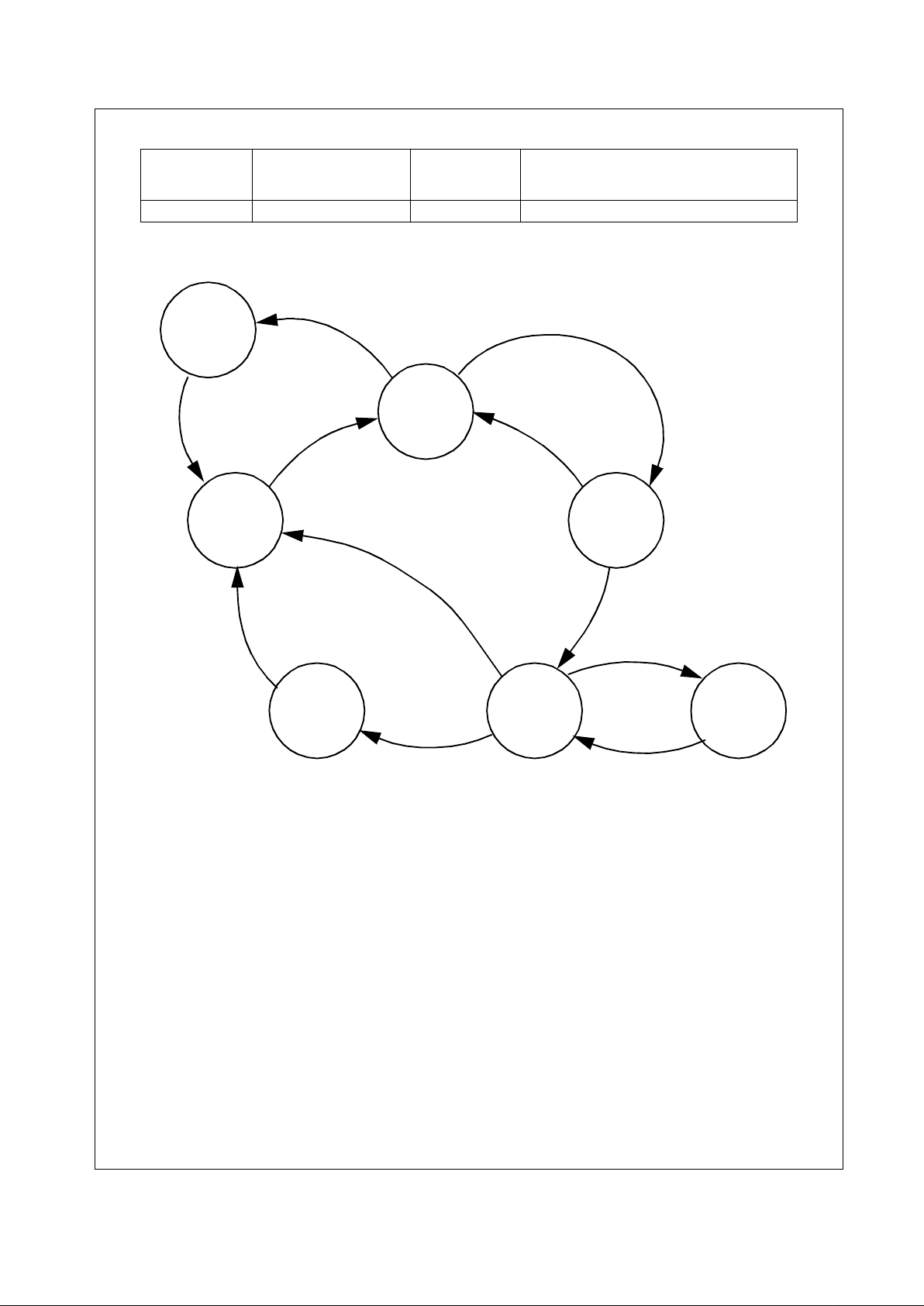
3.0 Functional Description
(Continued)
26
www.national.com
Figure 3-16 Transmit State Di agram
3.13.3.2 Transmit Data Flow without Priority Queueing
In the DP83820 transmit architecture without Priority
Queueing, packet transmission involves the following
steps:
1. The device driver receives packets from an upper
layer.
2. An available DP83820 transmit descriptor is
allocated. The fragment information is copied from
the NOS specific data structure(s) to the next
DP83820 transmit descriptor .
3. The driver adds this descriptor to it’s internal li st of
transmit descr ipt ors awaiting transmission.
4. If the internal list was empty (this descriptor
represents the only outstanding transmit packet),
then the driver must set the TXDP register to the
address of this descriptor, else the driver will append
this descriptor to the end of the list.
5. The driver sets the TXEN bit in the CR register to
insure that the transmit state machine is active.
6. If idle, the transmit st ate machine reads the des criptor
into the TxDescript orCache. If the OWN bit is not set ,
the trans mi t sta te ma chi ne re turn s to id le to wait for
TXEN to be set again.
7. The state machine then moves through the fragment
described wi thin the descriptor, filling the TxDataFifo
with data. The hardware handles all aspects of byte
alignment; no alignment is assumed. Fragments
may start and/or end on any byte address. The
transmit state machine uses the fragment pointer
and the SIZE field from the
cmdsts
field of the
current descr iptor to keep the TxDataFifo full. It also
uses the MORE bit and the SIZE field from the
cmdsts
field of the current descriptor to know when
packet boundaries occur.
8. When a packet has completed transmission
(successful or unsuccessful), the state machine
updates the
cmdsts
field of the current descriptor in
main memory (by bus-mastering a single 32-bit
word), relinquishing ownership, and indicating the
packet complet ion stat us. If mor e than one des criptor
txAdvance link != NULL txDescRead TXDP <- txDescCache.link. Clear CTDD. Start a
burst transfer at address TXDP with a length
derived from TXCFG.
link == NULL txIdle set CTDD. set ISR:TXIDLE.
txDescRefr
txIdle
txDescRead
txFifoBlocktxDescWrite
txAdvance
txFragRead
CR:TXEN && CTDD
CR:TXEN && !CTDD
XferDone
XferDone
XferDone
XferDone && OWN
XferDone && !OWN
|| link != NULL
descCnt == 0 && !(cmdsts & MORE)
descCnt == 0 && (cmdsts & MORE)
FifoAvail
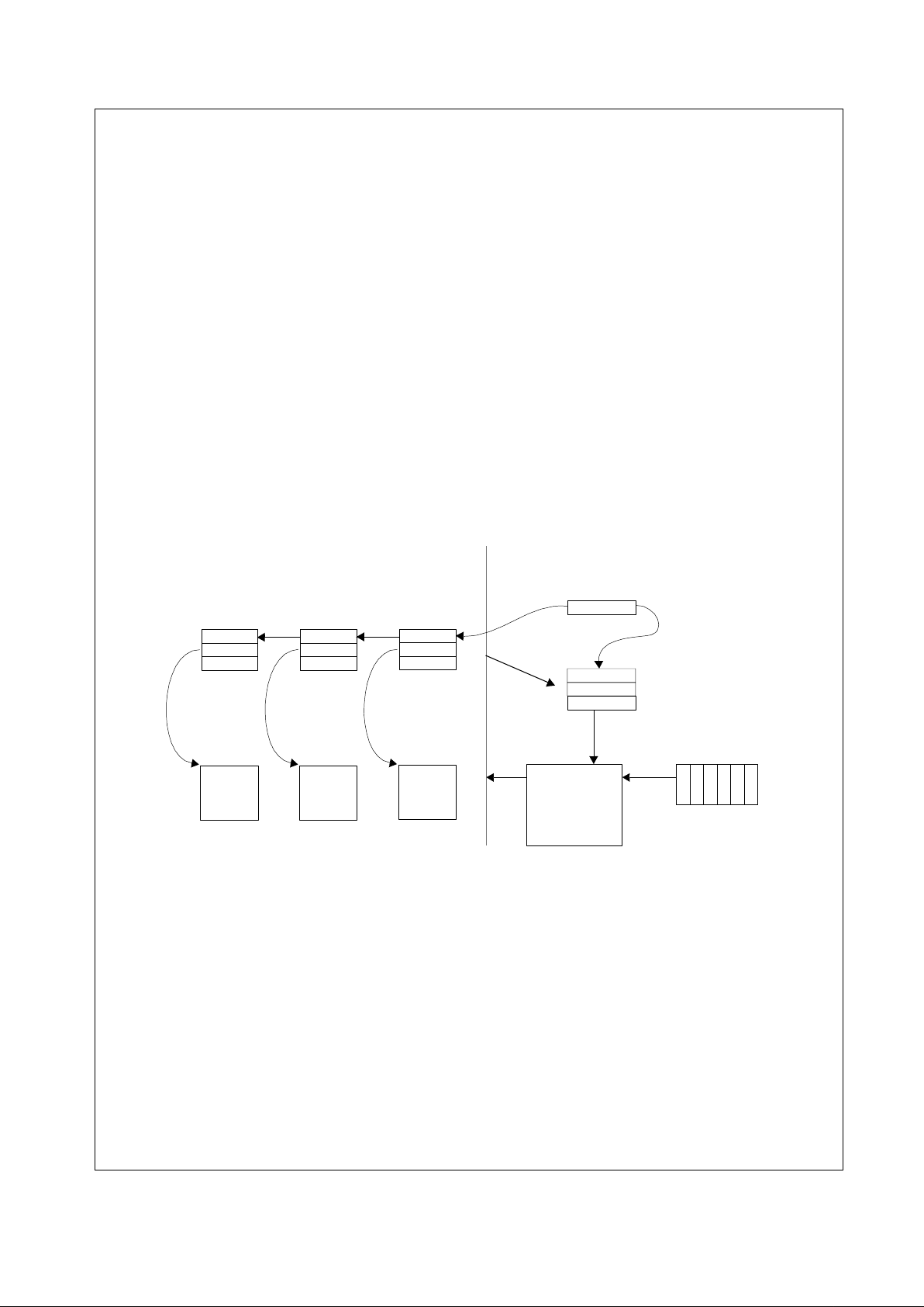
3.0 Functional Description
(Continued)
27
www.national.com
was used to describe the packet, then completion
status is updated only in the last descriptor.
Intermediate descriptors only have the OWN bits
modified.
9. If the link field of the descriptor is non-zero, the state
machine advances to the next descriptor and
continues. When reading the next descriptor, if the
OWN b it is not s et, the s tate mach ine will halt and
wait for TXEN to be set again.
10. If the link field is NULL, the transm it state machine
suspends, wait ing for t he TXEN b it in t he CR r egiste r
to be set. If the TXDP r egiste r is written t o, t he CTDD
flag will be cleared. When the TXEN bit is set, the
state machine will examine CTDD. If CTDD is set,
the state machine will "refresh" the link field of the
current descriptor. It will then follow the link field to
any new descriptor s that have bee n added to the end
of the list. If CTDD is clear (implying that TXDP has
been written to), the state machine will start by
reading in the descri ptor pointed to by TXDP.
3.13.3 .3 T ransmit Data Flow with Priority Queueing
The transmit architecture with Priority Queueing is the
same with a few min or di fferences:
— Driver keeps a separate list for each descriptor queue.
— When setting the TXEN bit, the driver must also set the
appropriate TXPRI bit for the prior ity queu e or queues to
which descriptors are being appended.
— Upon completion of a packet , the t ransm it state mach ine
first determines what the highest priority descriptor is
available based on non-zero link fields and TXEN bits. It
then follows the appropriate link or reads a new
descriptor for the next packet to be transmitted.
3.13.4 Receive Architecture
The receive architecture is as "symmetrical" to the transmit
architecture as possible. As is done in the transmitter, the
receive architecture can support a single descriptor queue
or multiple descriptor queues for handling priority traffic.
When the amount of receive data in the RxDataFIFO is
more than the RxDrainThreshold, or the RxDataFIFO
contains a complete packet, then the state machine begins
filling received buffers in host memo ry.
Figure 3-17 Receive Architecture without Priority Queuei ng
Without Priority Queueing, the device will transfer packets
to a single Descriptor list. Only one descriptor pointer is
required. The receive buffer manager prefetches receive
descriptors to prepare for incoming packets. When the
RXEN bit is set to 1 in the CR register (regardless of the
current state), and the DP83820 recei ve stat e machine is
idle, then DP83820 will read the contents of the descriptor
referenced by RXDP into the Rx Descriptor Cache. The Rx
Descriptor Cache allows the DP83820 to read an entire
descriptor in a single burst, and reduces the number of bus
accesses required for fragment information to 1. The
DP83820 Rx Descriptor Cache holds a single buffer
pointer/count combination.
Recieve Descriptor List
Current Rx Desc Ptr
Software/Memory Hardware
Rx Data FIFO
link
bufptr
cmdsts
cmdsts
Rx DMA
bufptr
Packet
RxHead
link
Rx Desc Cache
link
bufptr
cmdsts
Packet
link
bufptr
cmdsts
Packet
 Loading...