

NSC DP83815DUJB-AB, DP83815DVNG-AP, DP83815DVNG-AB, DP83815DUJB-PXE, DP83815DUJB-AP Datasheet
DP83815 10/100 Mb/s I ntegrated PCI Ethern et Media Access Control ler and Physical Layer (MacPhyter™)
© 2002 National Semiconductor Corporation www.national.com
1
September 2002
DP83815 10/100 Mb/s Integrated PCI Ethernet Media Access
Controller and Physical Layer (MacPhyter
™
)
General Description
DP83815 is a single-chip 10/100 Mb/s Ethernet Controller
for the PCI bus. It is targeted at low-cost, high volume PC
mother boards, adapter cards, and embedded systems.
The DP83815 fully implements the V2.2 33 MHz PCI bus
interface for host co mm un ica t io ns with power management
support. Packet descriptors and data are transferred via
bus-mastering, reducing the burden on the host CPU. The
DP83815 can support full duplex 10/100 Mb /s transmission
and reception, with minimum interframe gap.
The DP83815 device is an integration of an enhanced
version of the National Semiconductor PCI MAC/BIU
(Media Access Controller/Bus Interface Unit) and a 3.3V
CMOS physical layer interface.
Features
— IEEE 802.3 Compliant, PCI V2.2 MAC/BIU supports
traditional data rates of 10 Mb/s Ethernet and 100 Mb/s
Fast Ethernet (via internal phy)
— Bus master - burst sizes of up to 128 dwords (512 by tes)
— BIU compliant with PC 97 and PC 98 Hardware Design
Guides, PC 99 Hardware Design Guide draft, ACPI v1. 0,
PCI Power Management Specification v1.1, OnNow
Device Class Power Management Reference
Specification - Network Device Class v1.0a
— Wake on LAN (WOL) support compliant with PC98,
PC99, SecureOn, and OnNow, including directed
packets, Magic Packet, VLAN packets, ARP packets,
pattern match packets, and Phy status change
— Clkrun function for PCI Mobile Design Guide
— Virtual LAN (VLAN) and long frame support
— Support for IEEE 802.3x Full duplex flow control
— Extremely flexible Rx packet filtration including: single
address perfect filter with MSb masking, broadcast, 512
entry multicast/unicast hash table, deep packet pattern
matching for up to 4 unique patterns
— Statistics gathered for support of RFC 1213 (MIB II),
RFC 1398 (Ether-like MIB), IEEE 802.3 LME, reducing
CPU overhead for management
— Internal 2 KB Transmit and 2 KB Receive data FIFOs
— Serial EEPROM port with auto-load of configu ration da ta
from EEPROM at power-on
— Flash/PROM interface for remote boot support
— Fully integrated IEEE 802 .3/802.3u 3.3V CMOS physical
layer
— IEEE 802.3 10BASE-T transceiver with integrated filters
— IEEE 802.3u 100BASE-TX transceiver
— Fully integrated ANSI X3.263 compliant TP-PMD
physical sublayer with adaptive equalization and
Baseline Wander compensation
— IEEE 802.3u Auto-Negotiation - advertised features
configurable via EEPROM
— Full Duplex support for 10 and 100 Mb/s data rates
— Single 25 MHz reference clock
— 144-pin LQFP and 160-pin LBGA packages
— Low power 3.3V CMOS d es ign with ty pic al co nsu mp tion
of 561 mW operating, 380 mW during WOL mode, 33
mW sleep mode
— IEEE 802.3u MII for connecting alternative external
Physical Layer Devices
System Diagram
PCI Bus
DP83815
EEPROM
Isolation
10/100 Twisted Pair
BIOS ROM
(optional)
(optional)
TRI-STATE® is a registered trademark of National Semiconductor Corporation.
Magic Packet is a trademark of Advanced Micro Devices, Inc.

2 www.national.com
DP83815
Table of Contents
1.0 Connection Diagram . . . . . . . . . . . . . . . . . . 4
1.1 144 LQFP Package (VNG) . . . . . . . . . . . . 4
1.2 160 pin LBGA Package (UJB) . . . . . . . . . . 5
2.0 Pin Description . . . . . . . . . . . . . . . . . . . . . . 6
3.0 Functional Description . . . . . . . . . . . . . . . 13
3.1 MAC/BIU . . . . . . . . . . . . . . . . . . . . . . . . . 14
3.1.1 PCI Bus Interfa ce . . . . . . . . . . . . . . . . . . . . . . . . . . 14
3.1.2 T x M A C . . . . . . . . . . . . . . . . . . . . . . . . . . . . . . . . .15
3.1.3 Rx M AC . . . . . . . . . . . . . . . . . . . . . . . . . . . . . . . . .15
3.2 Buffer Management . . . . . . . . . . . . . . . . . 15
3.2.1 Tx Buffer Manager . . . . . . . . . . . . . . . . . . . . . . . . .15
3.2.2 Rx Buffer Manager . . . . . . . . . . . . . . . . . . . . . . . . .15
3.2.3 Packet Recognition . . . . . . . . . . . . . . . . . . . . . . . .15
3.2.4 MI B . . . . . . . . . . . . . . . . . . . . . . . . . . . . . . . . . . . .16
3.3 Interface Definitions . . . . . . . . . . . . . . . . . 16
3.3.1 PCI System Bus . . . . . . . . . . . . . . . . . . . . . . . . . . . 16
3.3.2 Boo t PROM . . . . . . . . . . . . . . . . . . . . . . . . . . . . . . 16
3.3.3 EE PR OM . . . . . . . . . . . . . . . . . . . . . . . . . . . . . . . . 16
3.3.4 Cl o c k . . . . . . . . . . . . . . . . . . . . . . . . . . . . . . . . . . .16
3.4 Physical Layer . . . . . . . . . . . . . . . . . . . . . 18
3.4.1 Auto-Negotiation . . . . . . . . . . . . . . . . . . . . . . . . . .18
3.4.2 Auto-Negotiation Register Control . . . . . . . . . . . . .18
3.4.3 Auto-Negotiation Parallel Detection . . . . . . . . . . . .18
3.4.4 Auto-Negotiation Restart . . . . . . . . . . . . . . . . . . . .19
3.4.5 Enabling Auto-Negotiation via Software . . . . . . . .19
3.4.6 Auto-Negotiation Complete Time . . . . . . . . . . . . . .19
3.5 LED Interfaces . . . . . . . . . . . . . . . . . . . . . 19
3.6 Half Duplex vs. Full Duplex . . . . . . . . . . . 20
3.7 Phy Loopback . . . . . . . . . . . . . . . . . . . . . 20
3.8 Status Information . . . . . . . . . . . . . . . . . . 20
3.9 100BASE-TX TRANSMITTER . . . . . . . . . 20
3.9.1 Code-group Encoding and Injection . . . . . . . . . . .21
3.9.2 Sc r a mb l e r . . . . . . . . . . . . . . . . . . . . . . . . . . . . . . . 2 1
3.9.3 NRZ to NRZI Encoder . . . . . . . . . . . . . . . . . . . . . .22
3.9.4 Binary to MLT-3 Convertor / Common Driver . . . . 22
3.10 100BASE-TX Receiver . . . . . . . . . . . . . . 23
3.10.1 Input and Base Line Wander Compensation . . . .23
3.10.2 Signal Detect . . . . . . . . . . . . . . . . . . . . . . . . . . . .23
3.10.3 Digital Adaptive Equalization . . . . . . . . . . . . . . . .25
3.10.4 Line Quality Monitor . . . . . . . . . . . . . . . . . . . . . . .26
3.10.5 MLT-3 to NRZI Decoder . . . . . . . . . . . . . . . . . . . .26
3.10.6 Clock Recovery Module . . . . . . . . . . . . . . . . . . . .27
3.10.7 NRZI to N R Z . . . . . . . . . . . . . . . . . . . . . . . . . . . . . 27
3.10.8 Seria l to Pa r a l l e l . . . . . . . . . . . . . . . . . . . . . . . . . . 27
3.10.9 De-scrambler . . . . . . . . . . . . . . . . . . . . . . . . . . . . 27
3.10.10 Code-group Alignment . . . . . . . . . . . . . . . . . . . .27
3.10.11 4B/5B Decoder . . . . . . . . . . . . . . . . . . . . . . . . . .27
3.10.12 100BASE-TX Link Integrity Monitor . . . . . . . . . .27
3.10.13 Bad SSD Detection . . . . . . . . . . . . . . . . . . . . . . 27
3.11 10BASE-T Transceiver Module . . . . . . . . 28
3.11.1 Operational Modes . . . . . . . . . . . . . . . . . . . . . . . .28
3.11.2 Smart Squelch . . . . . . . . . . . . . . . . . . . . . . . . . . .28
3.11.3 Coll i si o n D etection . . . . . . . . . . . . . . . . . . . . . . . . 28
3.11.4 Normal Link Pulse Detection/Generation . . . . . . .28
3.11.5 Jabber Function . . . . . . . . . . . . . . . . . . . . . . . . . .29
3.11.6 Autom a t ic Link Polarit y D e te ction . . . . . . . . . . . . . 29
3.11.7 10BASE-T Internal Loopback . . . . . . . . . . . . . . . .29
3.11.8 Transmit and Receive Filtering . . . . . . . . . . . . . . .29
3.11.9 Tran s m i t te r . . . . . . . . . . . . . . . . . . . . . . . . . . . . . . 2 9
3.11.10 Rec e i v e r . . . . . . . . . . . . . . . . . . . . . . . . . . . . . . .29
3.11.11 Far End Fault Indication . . . . . . . . . . . . . . . . . . . 29
3.12 802.3u MII . . . . . . . . . . . . . . . . . . . . . . . . 29
3.12.1 MII Access Configuration . . . . . . . . . . . . . . . . . . .29
3.12.2 MII Serial Management . . . . . . . . . . . . . . . . . . . . 29
3.12.3 MII Serial Management Access . . . . . . . . . . . . . 30
3.12.4 Serial Management Access Protocol . . . . . . . . . 30
3.12.5 Nibble-wide MII Data Inter face . . . . . . . . . . . . . . 30
3.12.6 Collision Detection . . . . . . . . . . . . . . . . . . . . . . . 31
3.12.7 Carrier Sense . . . . . . . . . . . . . . . . . . . . . . . . . . . 31
4.0 Register Set . . . . . . . . . . . . . . . . . . . . . . . . 32
4.1 Configuration Registers . . . . . . . . . . . . . . 32
4.1.1 Configuration Identification Register . . . . . . . . . . . 32
4.1.2 Configuration Command and Status Register . . . 33
4.1.3 Configuration Revision ID Register . . . . . . . . . . . 34
4.1.4 Configuration Latency Timer Register . . . . . . . . . 35
4.1.5 Configuration I/O Base Address Register . . . . . . . 35
4.1.6 Configuration Memory Address Register . . . . . . . 36
4.1.7 Configuration Subsystem Identification Register . 36
4.1.8 Boot ROM Configuration Register . . . . . . . . . . . . 37
4.1.9 Capabilities Pointer Register . . . . . . . . . . . . . . . . 37
4.1.10 Configuration Interrupt Select Register . . . . . . . . 38
4.1.11 Power Management Capabilities Register . . . . . 38
4.1.12 Power Management Control and Status Register 39
4.2 Operational Registers . . . . . . . . . . . . . . . 40
4.2.1 Command Register . . . . . . . . . . . . . . . . . . . . . . . . 41
4.2.2 Configuration and Media Status Register . . . . . . . 42
4.2.3 EEPROM Access Register . . . . . . . . . . . . . . . . . . 44
4.2.4 EEPROM Map . . . . . . . . . . . . . . . . . . . . . . . . . . . 44
4.2.5 PCI Test Control Register . . . . . . . . . . . . . . . . . . . 45
4.2.6 Interrupt Status Register . . . . . . . . . . . . . . . . . . . . 46
4.2.7 Interrupt Mask Register . . . . . . . . . . . . . . . . . . . . 47
4.2.8 Interrupt Enable Register . . . . . . . . . . . . . . . . . . . 49
4.2.9 Transmit Descriptor Pointer Regi ster . . . . . . . . . . 49
4.2.10 Transmit Configuration Register . . . . . . . . . . . . . 50
4.2.11 Receive Descriptor Pointer Regis ter . . . . . . . . . . 51
4.2.12 Receive Configuration Register . . . . . . . . . . . . . 52
4.2.13 CLKRUN Control/Status Regis te r . . . . . . . . . . . . 53
4.2.14 Wake Command/Status Register . . . . . . . . . . . . 55
4.2.15 Pause Control/Status Register . . . . . . . . . . . . . . 57
4.2.16 Receive Filter/Match Control Register . . . . . . . . 58
4.2.17 Receive Filter/Mat ch Data Regis ter . . . . . . . . . . 59
4.2.18 Receive Filter Logic . . . . . . . . . . . . . . . . . . . . . . 60
4.2.19 Boot ROM Address Regis te r . . . . . . . . . . . . . . . . 64
4.2.20 Boot ROM Data Register . . . . . . . . . . . . . . . . . . 64
4.2.21 Silicon Revision Registe r . . . . . . . . . . . . . . . . . . 64
4.2.22 Management Information Base Control Register 65
4.2.23 Management Information Base Registers . . . . . . 66
4.3 Internal PHY Registers . . . . . . . . . . . . . . . 67
4.3.1 Basic Mode Control Register . . . . . . . . . . . . . . . . 67
4.3.2 Basic Mode Status Register . . . . . . . . . . . . . . . . . 68
4.3.3 PHY Identifier Register #1 . . . . . . . . . . . . . . . . . . 69
4.3.4 PHY Identifier Register #2 . . . . . . . . . . . . . . . . . . 69
4.3.5 Auto-Negotiation Advertisement Register . . . . . . 69
4.3.6 Auto-Negotiation Link Partner Ability Register . . . 70
4.3.7 Auto-Negotiate Expansion Register . . . . . . . . . . . 71
4.3.8 Auto-Negotiation Next Page Transmit Register . . 71
4.3.9 PHY Status Register . . . . . . . . . . . . . . . . . . . . . . . 72
4.3.10 MII Interrupt Contr o l Regis ter . . . . . . . . . . . . . . . 74
4.3.11 MII Interrupt Status and Misc. Control Register . 74
4.3.12 False Carrier Sense Counter Register . . . . . . . . 75
4.3.13 Receiver Error Counter Register . . . . . . . . . . . . . 75
4.3.14 100 Mb/s PCS Configuration and Status Register 75
4.3.15 PHY Control Register . . . . . . . . . . . . . . . . . . . . . 76
4.3.16 10BASE-T Stat us/Control Register . . . . . . . . . . . 77
4.4 Recommended Registers Configuration .78
5.0 Buffer Management . . . . . . . . . . . . . . . . . .79
5.1 Overview . . . . . . . . . . . . . . . . . . . . . . . . .79
5.1.1 Descriptor Format . . . . . . . . . . . . . . . . . . . . . . . . . 79

3 www.national.com
DP83815
5.1.2 Single Descriptor Packets . . . . . . . . . . . . . . . . . . .81
5.1.3 Multiple Descriptor Packets . . . . . . . . . . . . . . . . . .82
5.1.4 De s criptor List s . . . . . . . . . . . . . . . . . . . . . . . . . . . 82
5.2 Transmit Architecture . . . . . . . . . . . . . . . 83
5.2.1 Transmit State Machine . . . . . . . . . . . . . . . . . . . . . 83
5.2.2 Transmit Data Flow . . . . . . . . . . . . . . . . . . . . . . . .85
5.3 Receive Architecture . . . . . . . . . . . . . . . . 86
5.3.1 Receive State Machine . . . . . . . . . . . . . . . . . . . . . 86
5.3.2 Re c e i v e D a t a Fl o w . . . . . . . . . . . . . . . . . . . . . . . . . 88
6.0 Power Management and Wake-On-LAN. . 89
6.1 Introduction . . . . . . . . . . . . . . . . . . . . . . . 89
6.2 Definitions (for this document only) . . . . . 89
6.3 Packet Filtering . . . . . . . . . . . . . . . . . . . . 89
6.4 Power Management . . . . . . . . . . . . . . . . 89
6.4.1 D0 S ta t e . . . . . . . . . . . . . . . . . . . . . . . . . . . . . . . . .90
6.4.2 D1 S ta t e . . . . . . . . . . . . . . . . . . . . . . . . . . . . . . . . .90
6.4.3 D2 S ta t e . . . . . . . . . . . . . . . . . . . . . . . . . . . . . . . . .90
6.4.4 D3hot State . . . . . . . . . . . . . . . . . . . . . . . . . . . . . .90
6.4.5 D3 c o l d St a te . . . . . . . . . . . . . . . . . . . . . . . . . . . . . 90
6.5 Wake-On-LAN (WOL) Mode . . . . . . . . . . 90
6.5.1 Entering WOL Mode . . . . . . . . . . . . . . . . . . . . . . .90
6.5.2 W a ke Ev e n t s . . . . . . . . . . . . . . . . . . . . . . . . . . . . . 91
6.5.3 Exiting WOL Mode . . . . . . . . . . . . . . . . . . . . . . . . 91
6.6 Sleep Mode . . . . . . . . . . . . . . . . . . . . . . .91
6.6.1 Entering Sleep Mode . . . . . . . . . . . . . . . . . . . . . . 91
6.6.2 Exiting Sleep Mode . . . . . . . . . . . . . . . . . . . . . . . . 91
6.7 Pin Configuration for Power Management 91
7.0 DC and AC Specifications . . . . . . . . . . . . . 92
7.1 DC Specifications . . . . . . . . . . . . . . . . . . . 92
7.2 AC Specifications . . . . . . . . . . . . . . . . . . . 93
7.2.1 PCI Clock Timing . . . . . . . . . . . . . . . . . . . . . . . . . 93
7.2.2 X1 Clock Timing . . . . . . . . . . . . . . . . . . . . . . . . . . 93
7.2.3 Power On Reset (PCI Active) . . . . . . . . . . . . . . . . 94
7.2.4 Non Power On Reset . . . . . . . . . . . . . . . . . . . . . . 94
7.2.5 POR PCI Inactive . . . . . . . . . . . . . . . . . . . . . . . . . 95
7.2.6 PCI Bus Cycles . . . . . . . . . . . . . . . . . . . . . . . . . . . 96
7.2.7 EE PR O M Auto-Load . . . . . . . . . . . . . . . . . . . . . 101
7.2.8 Boot PROM/FLASH . . . . . . . . . . . . . . . . . . . . . . 102
7.2.9 100BASE-TX Transmit . . . . . . . . . . . . . . . . . . . 103
7.2.10 10BASE-T Transmit End of Packet . . . . . . . . . 104
7.2.11 10 Mb/s Jabber Timing . . . . . . . . . . . . . . . . . . 104
7.2.12 10BASE-T Normal Link Pulse . . . . . . . . . . . . . 105
7.2.13 Auto-Negotiation Fast Link Pulse (FLP) . . . . . . 105
7.2.14 Media Independent Interface (MII . . . . . . . . . . . 106
List of Figures
Figure 3-1 DP83815 Functional Block Diagram . . . . . . . . . . . . . . . . . . . . . . . . . . . . . . . . . . . . . . . . . . . . . .13
Figure 3-2 MAC/BIU Functional Block Diagram . . . . . . . . . . . . . . . . . . . . . . . . . . . . . . . . . . . . . . . . . . . . . .14
Figure 3-3 Ethernet Packet Format. . . . . . . . . . . . . . . . . . . . . . . . . . . . . . . . . . . . . . . . . . . . . . . . . . . . . . . .16
Figure 3-4 DSP Physical Layer Block Diagram. . . . . . . . . . . . . . . . . . . . . . . . . . . . . . . . . . . . . . . . . . . . . . .17
Figure 3-5 LED Loading Example. . . . . . . . . . . . . . . . . . . . . . . . . . . . . . . . . . . . . . . . . . . . . . . . . . . . . . . . .19
Figure 3-6 100BASE-TX Transmit Block Diagram . . . . . . . . . . . . . . . . . . . . . . . . . . . . . . . . . . . . . . . . . . . .21
Figure 3-7 Binary to MLT-3 conversion. . . . . . . . . . . . . . . . . . . . . . . . . . . . . . . . . . . . . . . . . . . . . . . . . . . . .22
Figure 3-8 100 M/bs Receive Block Diagram . . . . . . . . . . . . . . . . . . . . . . . . . . . . . . . . . . . . . . . . . . . . . . . .24
Figure 3-9 100BASE-TX BLW Event Diagram . . . . . . . . . . . . . . . . . . . . . . . . . . . . . . . . . . . . . . . . . . . . . . .25
Figure 3-10 EIA/TIA Attenuation vs. Frequency for 0, 50, 100, 130 & 150 meters of CAT V cable . . . . . . . .26
Figure 3-11 MLT-3 Signal Measured at AII after 0 meters of CAT V cable. . . . . . . . . . . . . . . . . . . . . . . . . . .26
Figure 3-12 MLT-3 Signal Measured at AII after 50 meters of CAT V cable. . . . . . . . . . . . . . . . . . . . . . . . . .26
Figure 3-13 MLT-3 Signal Measured at AII after 100 meters of CAT V cable. . . . . . . . . . . . . . . . . . . . . . . . .26
Figure 3-14 10BASE-T Twisted Pair Smart Squelch Operation . . . . . . . . . . . . . . . . . . . . . . . . . . . . . . . . . . .28
Figure 3-15 Typical MDC/MDIO Read Operation . . . . . . . . . . . . . . . . . . . . . . . . . . . . . . . . . . . . . . . . . . . . . .30
Figure 3-16 Typical MDC/MDIO Write Operation . . . . . . . . . . . . . . . . . . . . . . . . . . . . . . . . . . . . . . . . . . . . . .31
Figure 4-1 Pattern Buffer Memory - 180h words (word = 18bits) . . . . . . . . . . . . . . . . . . . . . . . . . . . . . . . . .61
Figure 4-2 Hash Table Memory - 40h bytes addressed on word boundaries. . . . . . . . . . . . . . . . . . . . . . . .63
Figure 5-1 Single Descriptor Packets . . . . . . . . . . . . . . . . . . . . . . . . . . . . . . . . . . . . . . . . . . . . . . . . . . . . . .81
Figure 5-2 Multiple Descriptor Packets . . . . . . . . . . . . . . . . . . . . . . . . . . . . . . . . . . . . . . . . . . . . . . . . . . . . .82
Figure 5-3 List and Ring Descriptor Organization. . . . . . . . . . . . . . . . . . . . . . . . . . . . . . . . . . . . . . . . . . . . .82
Figure 5-4 Transmit Architecture. . . . . . . . . . . . . . . . . . . . . . . . . . . . . . . . . . . . . . . . . . . . . . . . . . . . . . . . . .83
Figure 5-5 Transmit State Diagram. . . . . . . . . . . . . . . . . . . . . . . . . . . . . . . . . . . . . . . . . . . . . . . . . . . . . . . .84
Figure 5-6 Receive Architecture . . . . . . . . . . . . . . . . . . . . . . . . . . . . . . . . . . . . . . . . . . . . . . . . . . . . . . . . . .86
Figure 5-7 Receive State Diagram . . . . . . . . . . . . . . . . . . . . . . . . . . . . . . . . . . . . . . . . . . . . . . . . . . . . . . . .88
List of Tables
Table 3-1 4B5B Code-Group Encoding/Decoding. . . . . . . . . . . . . . . . . . . . . . . . . . . . . . . . . . . . . . . . . . . .22
Table 3-2 Typical MDIO Frame Format . . . . . . . . . . . . . . . . . . . . . . . . . . . . . . . . . . . . . . . . . . . . . . . . . . . .30
Table 4-1 Configuration Register Map. . . . . . . . . . . . . . . . . . . . . . . . . . . . . . . . . . . . . . . . . . . . . . . . . . . . .32
Table 4-2 Operational Register Map . . . . . . . . . . . . . . . . . . . . . . . . . . . . . . . . . . . . . . . . . . . . . . . . . . . . . .40
Table 4-3 MIB Registers . . . . . . . . . . . . . . . . . . . . . . . . . . . . . . . . . . . . . . . . . . . . . . . . . . . . . . . . . . . . . . .66
Table 5-1 DP83815 Descriptor Format . . . . . . . . . . . . . . . . . . . . . . . . . . . . . . . . . . . . . . . . . . . . . . . . . . . .79
Table 5-2 cmdsts Common Bit Definitions. . . . . . . . . . . . . . . . . . . . . . . . . . . . . . . . . . . . . . . . . . . . . . . . . .79
Table 5-3 Transmit Status Bit Definitions. . . . . . . . . . . . . . . . . . . . . . . . . . . . . . . . . . . . . . . . . . . . . . . . . . . 80
Table 5-4 Receive Status Bit Definitions . . . . . . . . . . . . . . . . . . . . . . . . . . . . . . . . . . . . . . . . . . . . . . . . . . . 81
Table 5-5 Transmit State Tables . . . . . . . . . . . . . . . . . . . . . . . . . . . . . . . . . . . . . . . . . . . . . . . . . . . . . . . . .84
Table 5-6 Receive State Tables. . . . . . . . . . . . . . . . . . . . . . . . . . . . . . . . . . . . . . . . . . . . . . . . . . . . . . . . . .87
Table 6-1 Power Management Modes. . . . . . . . . . . . . . . . . . . . . . . . . . . . . . . . . . . . . . . . . . . . . . . . . . . . .89
Table 6-2 PM Pin Configuration. . . . . . . . . . . . . . . . . . . . . . . . . . . . . . . . . . . . . . . . . . . . . . . . . . . . . . . . . .91

4 www.national.com
DP83815
1.0 Connection Diagram
1.1 144 LQFP Package (VNG)
Order Number DP83815DVNG
See NS Package Number VNG144A
121
122
123
124
125
126
127
128
129
130
131
132
99
98
97
96
95
94
93
92
91
90
89
88
87
86
85
84
83
82
81
80
79
78
77
76
75
74
73
66
65
64
63
62
61
60
59
58
57
56
55
54
53
52
51
50
49
48
47
46
45
44
43
42
41
123456789
10
11
12
13
14
15
16
17
18
19
20
21
22
23
24
25
26
27
28
30
31
323329
Identification
Pin1
37
38
39
40
120
119
118
117
116
115
114
113
112
110
109
111
DEVSELN
TRDYN
IRDYN
FRAMEN
CBEN2
AD16
AD17
AD18
STOPN
PERRN
SERRN
PAR
CBEN1
AD15
AD14
AD13
AD12
AD11
AD10
AD9
PCIVSS4
AD8
AD19
AD20
AD21
AD22
AD23
IDSEL
PCIVSS2
PCIVDD3
VSSIO4
PCIVDD4
VDDIO4
PCIVSS3
PCIVDD2
CBEN3
AD24
AD25
AD26
CBEN0
MACVSS1
MACVDD1
RESERVED
VREF
PCIVDD1
AD29
AD31
PCIVSS1
REQN
GNTN
RSTN
INTAN
AD28
PCICLK
AD30
PMEN/CLKRUNN
TXIOVSS2
TXIOVSS1
TPTDP
TPTDM
NC
RXAVDD2
RXAVSS2
TPRDP
TPRDM
SUBGND2
AD27
AD7
AD6
AD5
PCIVSS5
MA1/LED10N
MA2/LED100N
MA3/EEDI
MA4/EECLK
MA5
MWRN
MD4/EEDO
MD3
EESEL
AD0
AD1
AD2
AD3
AD4
MD0
MCSN
MD1/CFGDISN
MD2
MD5
MD6
MD7
MA0/LEDACTN
PCIVDD5
VSSIO2
VDDIO2
MACVSS2
MACVDD2
VDDIO5
VSSIO5
MDIO
MDC
RXCLK
RXD0/MA6
RXD1/MA7
RXD2/MA8
RXD3/MA9
RXOE
RXER/MA10
RXDV/MA11
TXD3/MA15
COL/MA16
CRS
TXEN
TXCLK
TXD2/MA14
TXD1/MA13
TXD0/MA12
VSSIO3
VDDIO3
VSSIO1
VDDIO1
X2
X1
DP83815
SUBGND3
PHYVSS1
PHYVDD1
NC
3VAUX
363534
67
68
69
70
71
72
100
101
102
103
104
105
106
107
108
144
143
142
141
140
139
138
137
136
135
134
133
RXAVSS1
RXAVDD1
PWRGOOD
MRDN
TXDVDD
FXVDD
FXVSS
PHYVSS2
PHYVDD2
SUBGND1
RESERVED
NC
NC
RESERVED
TXDVSS
5 www.national.com
1.0 Connection Diagram (Continued)
DP83815
1.2 160 pin LBGA Package (UJB)
Top View
Order Number DP83815DUJB
See NS Package Number UJB160A
Identification
Pin A1
A
B
C
D
E
F
G
H
J
K
L
M
N
P
1
2
3
4
5
6
7
8
9
10
11
12
13
14
(Marked on Top)

6 www.national.com
DP83815
2.0 Pin Description
PCI Bus Interface
Symbol
LQFP Pin
No(s)
LBGA Pin
No(s) Dir Description
AD[31-0] 66, 67, 68, 70,
71, 72, 73, 74,
78, 79, 81, 82,
83, 86, 87, 88,
101, 102, 104,
105, 106, 108,
109, 110, 112,
113, 115, 116,
118, 1 19, 120,
121
K3, K2, K4,
L3, L2, M1,
N3, P3, L4
N5, M5, L5,
N6, L6, N7,
P7, N10, L10,
M11, N11,
P12, N12,
M13, M14,
L12, L14,
K13, K14,
K11, J13, J14,
J12
I/O Address and Data: Multiplexed address and data bus. As a bus
master, the DP83815 will drive address during the first bus phase.
During subsequent phases, the DP83815 will either read or write
data expecting the target to increment its address pointer. As a bus
target, the DP83815 will decode each address on the bus and
respond if it is the target being addressed.
CBEN[3-0] 75,
89,
100,
111
N4,
L7,
M10,
L13
I/O Bus Command/Byte Enable: During the address phase these
signals define the “bus command” or the type of bus transaction that
will take place. During the data phase these pins indicate which byte
lanes contain valid data. CBEN[0] applies to byte 0 (bits 7-0) and
CBEN[3] applies to byte 3 (bits 31-24) in the Little Endian Mode. In
Big Endian Mode, CBEN[3] applies to byte 0 (bits 31-24) and
CBEN[0] applies to byte 3 (bits 7-0).
PCICLK 60 H4 I Clock: This PCI Bus clock provides timing for all bus phases. The
rising edge defines the start of each phase. The clock frequency
ranges from 0 to 33 MHz.
DEVSELN 95 P9 I/O Device Select: As a bus master, the DP83815 samples this signal to
insure that the destination address for the data transfer is recognized
by a PCI target. As a target, the DP83815 asserts this signal low
when it recognizes its address after FRAMEN is asserted.
FRAMEN 91 M7 I/O Frame: As a bus master, this signal is asserted low to indicate the
beginning and duration of a bus transaction. Data transfer takes
place when this signal is asserted. It is de-asserted before the
transaction is in its final phase. As a target, the device monitors this
signal before decoding the address to check if the current transaction
is addressed to it.
GNTN 63 J2 I Grant: This signal is asserted low to indicate to the DP83815 that it
has been granted ownership of the bus by the central arbiter. This
input is used when the DP83815 is acting as a bus master.
IDSEL 76 M4 I Initialization Device Select: This pin is sampled by the DP83815 to
identify when configuration read and write accesses are intended for
it.
INTAN 61 J1 O Interrupt A: This signal is asserted low when an interrupt condition
occurs as defined in the Interrupt Status Register, Interrupt Mask,
and Interrupt Enable registers.
IRDYN 92 P8 I/O Initiator Ready: As a bus master, this signal will be asserted low
when the DP83815 is ready to complete the current data phase
transaction. This signal is used in conjunction with the TRYDN
signal. Data transaction takes place at the rising edge of PCICLK
when both IRDYN and TRDYN are asserted low. As a target, this
signal indicates that the master has put the data on the bus.
PAR 99 P10 I/O Parity: This signal indicates even parity across AD[31-0] and
CBEN[3-0] including the PAR pin. As a master, PAR is asserted
during address and write data phases. As a target, PAR is asserted
during read data phases.

7 www.national.com
2.0 Pin Description (Continued)
DP83815
PERRN 97 N9 I/O Parity Error: The DP83815 as a master or target will assert this
signal low to indicate a parity error on any incoming data (except for
special cycles). As a bus master, it will monitor this signal on all write
operations (except for special cycles).
REQN 64 J4 O Request: The DP83815 will assert this signal low to request
ownership of the bus from the central arbiter.
RSTN 62 J3 I Reset: When this signal is asserted all outputs of DP83815 will be
tri-stated and the device will be put into a known state.
SERRN 98 L9 I/O System Error: This signal is asserted low by DP83815 during
address parity errors and system errors if enabled.
STOPN 96 M9 I/O Stop: This signal is asserted low by the target device to request the
master device to stop the current transaction.
TRDYN 93 N8 I/O Target Ready: As a master, this signal indicates that the target is
ready for the data during write operation and with the data during
read operation. As a target, this signal will be asserted low when the
(target) device is ready to complete the current data phase
transaction. This signal is used in conjunction with the IRDYN signal.
Data transaction takes place at the rising edge of PCICLK when both
IRDYN and TRDYN are asserted low.
PMEN/
CLKRUNN
59 H2 I/O Power Management Event/Clock Run Function : This pin is a dual
function pin. The function of this pin is determined by the
CLKRUN_EN bit 0 of the CLKRUN Control and Status register
(CCSR). Default operation of this pin is PMEN.
Power Management Eve nt: This signal is asserted low by DP83815
to indicate that a power management event has occurred. For pin
connection please refer to Section 6.7.
Clock Run Function: In this mode, this pin is used to indicate when
the PCICLK will be stopped.
3VAUX 122 J11 I PCI Auxiliary Voltage Sense: This pin is used to sense the
presence of a 3.3V auxiliary supply in order to define the PME
Support available. For pin connection please refer to Section 6.7.
This pin has an internal weak pull down.
PWRGOOD 123 H13 I PCI bus power good: Connected to PCI bus 3.3V power (not
3.3Vaux), this pin is used to sense the presence of PCI bus power.
This pin has an internal weak pull down.
PCI Bus Interface
Symbol
LQFP Pin
No(s)
LBGA Pin
No(s) Dir Description

8 www.national.com
2.0 Pin Description (Continued)
DP83815
Note: MII is normally tri-stated, unless enabled by CFG:EXT_PHY. See Section 4.2.2.
Media Independent Interface (MII)
Symbol
LQFP Pin
No(s)
LBGA Pin
No(s) Dir Description
COL 28 C5 I Collision Det e c t: The COL signal is asserted high asynchronously
by the external PMD upon detection of a collision on the medium. It
will remain asserted as long as the collision condition persists.
CRS 29 B5 I Carrier Sense: This signal is asserted high asynchronously by the
external PMD upon detection of a non-idle medium.
MDC 5 A11 O Management Data Clock: Clock signal with a maximum rate of 2.5
MHz used to transfer management data for the external PMD on the
MDIO pin.
MDIO 4 C11 I/O Management Data I/O: Bidirectional signal used to transfer
management information for the external PMD. (See Section 3.12.4
for details on connections when MII is used.)
RXCLK 6 D11 I Receive Clock: A continuous clock, sourced by an external PMD
device, that is recovered from the incoming data. During 100 Mb/s
operation RXCLK is 25 MHz and during 10 Mb/s this is 2.5 MHz.
RXD3/MA9,
RXD2/MA8,
RXD1/MA7,
RXD0/MA6
12,
11,
10,
7
A9,
B9,
D10,
B10
IOReceive Data: Sourced from an external PMD, that contains data
aligned on nibble boundaries and are driven synchronous to RXCLK.
RXD[3] is the most significant bit and RXD[0] is the least significant
bit.
BIOS ROM Address: During external BIOS ROM access, these
signals become part of the ROM address.
RXDV/MA11 15 B8 IOReceive Data Valid: Indicates that the external PMD is presenting
recovered and decoded nibbles on the RXD signals, and that RXCLK
is synchronous to the recovered data in 100 Mb/s operation. This
signal will encompass the frame, starting with the Start-of-Frame
delimiter (JK) and excluding any End-of-Frame delimiter (TR).
BIOS ROM Address: During external BIOS ROM access, this signal
becomes part of the ROM address.
RXER/MA10 14 D9 IOReceive Error: Asserted high synchronously by the external PMD
whenever it detects a media error and RXDV is asserted in 100 Mb/s
operation.
BIOS ROM Address: During external BIOS ROM access, this signal
becomes part of the ROM address.
RXOE 13 C9 O Receive Output Enable: Used to disable an external PMD while the
BIOS ROM is being accessed.
TXCLK 31 A4 I Transmit Clock: A continuous clock that is sourced by the external
PMD. During 100 Mb/s operation this is 25 MHz +/- 100 ppm. During
10 Mb/s operation this clock is 2.5 MHz +/- 100 ppm.
TXD3/MA15,
TXD2/MA14,
TXD1/MA13,
TXD0/MA12
25,
24,
23,
22
B6,
C6,
A6,
D7
OOTransmit Data: Signals which are driven synchronous to the TXCLK
for transmission to the external PMD. TXD[3] is the most significant
bit and TXD[0] is the least significant bit.
BIOS ROM Address: During external BIOS ROM access, these
signals become part of the ROM address.
TXEN 30 D5 O Transmit Enable: This signal is synchronous to TXCLK and
provides precise framing for data carried on TXD[3-0] for the external
PMD. It is asserted when TXD[3-0] contains valid data to be
transmitted.

9 www.national.com
2.0 Pin Description (Continued)
DP83815
Note: DP83815 supports NM27LV010 for the BIOS ROM interface device.
100BASE-TX/10BASE-T Interface
Symbol
LQFP Pin
No(s)
LBGA Pin
No(s) Dir Description
TPTDP,
TPTDM
54,
53
G1,
F1
A-O Transmit Data: Differential common output driver. This differential
common output is configurable to either 10BASE-T or 100BASE-TX
signaling:
10BASE-T: Transmission of Manchester encoded 10BASE-T packet
data as well as Link Pulses (including Fast Link Pulses for AutoNegotiation purposes).
100BASE-TX: Transmission of ANSI X3T12 compliant MLT-3 data.
The DP83815 will automatically configure this common output driver
for the proper signal type as a result of either forced configuration or
Auto-Negotiation.
TPRDP,
TPRDM
46,
45
D1,
C1
A-I Receive Data: Differential common input buffer. This differential
common input can be configured to accept either 100BASE-TX or
10BASE-T signaling:
10BASE-T: Reception of Manchester encoded 10BASE-T packet
data as well as normal Link Pulses and Fast Link Pulses for AutoNegotiation purposes.
100BASE-TX: Reception of ANSI X3T12 compliant scrambled MLT-3
data.
The DP83815 will automatically configure this common input buffer
to accept the proper signal type as a result of either forced
configuration or Auto-Negotiation.
BIOS ROM/Flash Interface
Symbol
LQFP Pin
No(s)
LBGA Pin
No(s) Dir Description
MCSN 129 G13 O BIOS ROM/Flash Chip Select: During a BIOS ROM/Flash
access, this signal is used to select the ROM device.
MD7, MD6, MD5,
MD4/EEDO, MD3,
MD2,
MD1/CFGDISN,
MD0
141, 140, 139,
138, 135,
134,
133,
132
D13,D12,D14,
E11, E14,
F11,
F13,
F12
I/O BIOS ROM/Flash Data Bus: During a BIOS ROM/Flash access
these signals are used to transfer data to or from the ROM/Flash
device.
MD[5:0] pins have internal weak pull ups.
MD6 and MD7 pins have internal weak pull downs.
MA5,
MA4/EECLK,
MA3/EEDI,
MA2/LED100LNK,
MA1/LED10LNK,
MA0/LEDACT
3,
2,
1,
144,
143,
142
B11,
A12,
B12,
C13,
C12,
C14
O BIOS ROM/Flash Address: During a BIOS ROM/Flash access,
these signals are used to drive the ROM/Flash address.
MWRN 131 F14 O BIOS ROM/Flash Writ e : During a BIOS ROM/Flash access, this
signal is used to enable data to be written to the Flash device.
MRDN 130 G11 O BIOS ROM/Flash Read: During a BIOS ROM/Flash access, this
signal is used to enable data to be read from the Flash device.

10 www.national.com
2.0 Pin Description (Continued)
DP83815
Note: DP83815 supports FM93C46 for the EEPROM device.
Clock Interface
Symbol
LQFP Pin
No(s)
LBGA Pin
No(s) Dir Description
X1 17 D8 I Crystal/Oscillator Input: This pin is the primary clock reference
input for the DP83815 and must be connected to a 25 MHz 0.005%
(50ppm) clock source. The DP83815 device supports either an
external crystal resonator connected across pins X1 and X2, or an
external CMOS-level oscillator source connected to pin X1 only.
X2 18 C7 O Crystal Output: This pin is used in conjunction with the X1 pin to
connect to an external 25 MHz crystal resonator device. This pin
must be left unconnected if an external CMOS oscillator clock source
is utilized. For more information see the definition for pin X1.
LED Interface
Symbol
LQFP Pin
No(s)
LBGA Pin
No(s) Dir Description
LEDACTN/MA0 142 C14 O TX/RX Activity: This pin is an output indicating transmit/receive
activity. This pin is driven low to indicate active transmission or
reception, and can be used to drive a low current LED (<6 mA). The
activity event is stretched to a min duration of approximately 50 ms.
LED100N/MA2 144 C13 O 100 Mb/s Link: This pin is an output indicating the 100 Mb/s Link
status. This pin is driven low to indicate Good Link status for 100
Mb/s operation, and can be used to drive a low current LED (<6 mA).
LED10N/MA1 143 C12 O 10 Mb/s Link: This pin is an output indicating the 10 Mb/s Link
status. This pin is driven low to indicate Good Link status for 10 Mb/s
operation, and can be used to drive a low current LED (<6 mA).
Serial EEPROM Interface
Symbol
LQFP Pin
No(s)
LBGA Pin
No(s) Dir Description
EESEL 128 G14 O EEPROM Chip Select: This signal is used to enable an external
EEPROM device.
EECLK/MA4 2 A12 O EEPROM Clock: During an EEPROM acce ss (E ESE L assert ed),
this pin is an output used to drive the serial clock to an external
EEPROM device.
EEDI/MA3 1 B12 O EEPROM Data In: During an EEPROM access (EESEL asserted),
this pin is an output used to drive opcode, address, and data to an
external serial EEPROM device.
EEDO/MD4 138 E11 I EEPROM Data Out: During an EEPROM access (EESEL asserted),
this pin is an input used to retrieve EEPROM serial read data.
This pin has an internal weak pull up.
MD1/CFGDISN 133 F13 I/O Configuration Disable: When pulled low at power-on time, disables
load of configuration data from the EEPROM. Use 1 KΩ to ground to
disable configuration load.

11 www.national.com
2.0 Pin Description (Continued)
DP83815
External Reference Interf ace
Symbol
LQFP Pin
No(s)
LBGA Pin
No(s) Dir Description
VREF 40 A2 I Bandgap Reference: External current reference resistor for internal
Phy bandgap circuitry. The value of this resistor is 9.31 KΩ 1% metal
film (100 ppm/
o
C) which must be connected from the VREF pin to
analog ground.
No Connects
Symbol
LQFP Pin
No(s)
LBGA Pin
No(s) Dir Description
NC 34, 42, 43, 48 A1, A13, A14,
B3, B13, B14,
D4, F3, F4,
G2, M2, M3,
N1, N2, N13,
N14, P1, P2,
P13, P14
No Connect
Reserved 41, 50, 127 D2, E3, H12 These pins are reserved and cannot be connected to any external
logic or net.

12 www.national.com
2.0 Pin Description (Continued)
DP83815
Supply Pins
Symbol
LQFP Pin
No(s)
LBGA Pin
No(s) Dir Description
SUBGND1,
SUBGND2,
SUBGND3
37,
49,
126
B2,
E1,
G12
S Substrate GND
RXAVDD1,
RXAVDD2
39,
47
C2,
E2
S RX Analog VDD - connect to isolated Aux 3.3V supply VDD
RXAVSS1,
RXAVSS2
38,
44
B1,
D3
S RX Analog GND
TXIOVSS1,
TXIOVSS2
52,
55
F2,
G4
S TX Output driver VSS
TXDVDD 56 H3 S TX Digital VDD - connect to Aux 3.3V supply VDD
TXDVSS 51 E4 S TX Digital VSS
MACVDD1,
MACVDD2
58,
125
H1,
H11
S Mac/BIU digital core VDD - connect to Aux 3.3V supply VDD
MACVSS1,
MACVSS2
57,
124
G3,
H14
S Mac/BIU digital core VSS
PCIVDD1,
PCIVDD2,
PCIVDD3,
PCIVDD4,
PCIVDD5
69,
80,
94,
107,
117
L1,
P5,
L8,
M12,
K12
S PCI IO VDD - connect to PCI bus 3.3V VDD
PCIVSS1,
PCIVSS2,
PCIVSS3,
PCIVSS4,
PCIVSS5
65,
77,
90,
103,
114
K1,
P4,
M8,
P11,
L11
S PCI IO VSS
VDDIO2,
VDDIO4
19,
85
C8,
M6
S Misc. IO VDD - connect to Aux 3.3V supply VDD
VDDIO1,
VDDIO3,
VDDIO5
9,
27,
137
C10,
A5,
E13
S Misc. IO VDD - connect to Aux 3.3V supply VDD
VSSIO2,
VSSIO4
16,
84
A8,
P6
SMisc. IO VSS
VSSIO1,
VSSIO3,
VSSIO5
8,
26,
136
A10,
D6,
E12
SMisc. IO VSS
PHYVDD1,
PHYVDD2
21,
33
B7,
B4
S Phy digital core VDD - connect to Aux 3.3V supply VDD
PHYVSS1,
PHYVSS2
20,
32
A7,
C4
S Phy digital core VSS
FSVDD 36 C3 S Frequency Synthesizer VDD - connect to isolated Aux 3.3V supply
VDD
FSVSS 35 A3 S Frequency Synthesizer VSS
13 www.national.com
DP83815
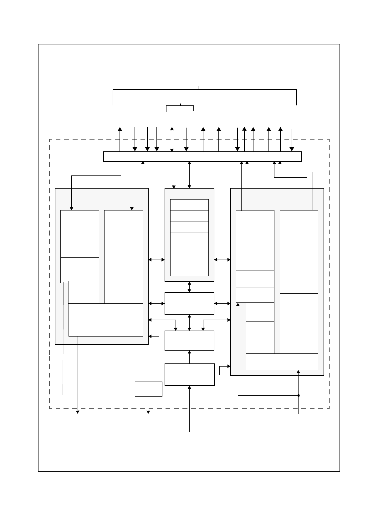
3.0 Functional Description
DP83815 consists of a MAC/BIU (Media Access
Controller/Bus Interface Unit), a physical layer interface,
SRAM, and miscellaneous support logic. The MAC/BIU
includes the PCI bus, BIOS ROM a nd EEPROM int erfaces ,
and an 802.3 MAC. The physical layer interface used is a
single-port version of the 3.3V DsPhyter. Internal memory
consists of one - 0.5 KB and two - 2 KB SRAM blocks.
Figure 3-1 DP83815 Functional Block Diagram
MAC/BIU
Interface
SRAM
25 MHz Clk
MII RX
MII TX
MII Mgt
BIOS ROM Cntl
BIOS ROM Data
BROM/EE
PCI AD
PCI CNTL
PCI CLK
3V DSP Physical Layer
Logic
RX-2 KB
SRAM
TX-2 KB
TPRDP/M
EEPROM/LEDs
MII TX
MII RX
MII Mgt
Test data in
Test data out
MII TX
MII RX
MII Mgt
TPTDP/M
DP83815
Tx Addr
Tx wr data
Rx Addr
Rx wr data
Rx rd data
Tx rd data
RAM
BIST
Logic
SRAM
RXFilter
.5 KB
3.0 Functional Description (Continued)
14 www.national.com
DP83815
Figure 3-2 MAC/BIU Functional Block Diagram
3.1 MAC/BIU
The MAC/BIU is a derivative design from the DP83810
(Euphrates). The original MAC/BIU design has been
optimized to improve logic efficiency and enhanced to add
features consistent with current market needs and
specification compliance. The MAC/BIU design blocks are
discussed in this section.
3.1.1 PCI Bus Interfac e
This block implements PCI v2.2 bus protocols, and
configuration space. Supports bus master reads and writes
to CPU memory, and CPU access to on-chip register
space. Additional functions provided include: configuration
control, serial EEPROM access with auto configuration
load, interrupt control, power management control with
support for PME or CLKRUN function.
3.1.1.1 Byte Ordering
The DP83815 can be configured to order the bytes of data
on the AD[31:0] bus to conform to little endian or big
endian ordering through the use of the Configuration
Register, bit 0 (CFG:BEM). By default, the device is in little
endian ordering. Byte ordering only affects data FIFOs.
Register information remains bit aligned (i.e. AD[31] maps
to bit 31 in any register space, AD[0] maps to bit 0, etc.).
Tx Buffer Manager
MIB
Tx MAC
Rx MAC
PCI Bus
Data FIFO
Physical Layer Interface
93C46
Serial
EEPROM
MAC/BIU
32
15
32
32
32
32
32
16
32
32
4
4
32
Rx Filter
Pkt Recog
Logic
SRAM
Rx Buffer Manager
Data FIFO
Boot ROM/
Flash
PCI Bus
Interface

3.0 Functional Description (Continued)
15 www.national.com
DP83815
Little Endian (CFG:BEM=0): The byte orientation for
receive and transmit data in system memory is as follows:
Big Endian (CFG:BEM=1): The byte orientation for
receive and transmit data in system memory is as follows:
3.1.1.2 PCI Bus Interrupt Control
PCI bus interrupts for the DP83815 are asynchronously
performed by asserting pin INTAN. This pin is an open
drain output. The sou rce of th e in terrupt can be determined
by reading the Interrupt Status Register (ISR). One or more
bits in the ISR will be set, denoting all currently pending
interrupts. Caution: Reading of the ISR clears ALL bits.
Masking of specified interrupts can be accomplished by
using the Interrupt Mask Register (IMR).
3.1.1.3 Timer
The Latency Timer described in CFGLAT:LAT defines the
minimum number of bus clocks that the device will hold the
bus. Once the device gains control of the bus and issues
FRAMEN, the Latency Timer will begin counting down. If
GNTN is de-asserted before the DP83815 has finished
with the bus, the device will maintain ownership of the bus
until the timer reaches zero (or has finished the bus
transfer). The timer is an 8-bit counter.
3.1.2 Tx MAC
This block implements the transmit portion of 802.3 Media
Access Control. The Tx MAC retrieves packet data from
the Tx Buffer Manager and sends it out through the
transmit portion. Additionally, the Tx MAC provides MIB
control information for transmit packets.
3.1.3 Rx MAC
This block implements the receive portion of 802.3 Media
Access Control. The Rx MAC retrieves packet data from
the receive portion and sends it to the Rx Buffer Manager.
Additionally, the Rx MAC provides MIB control information
and packet address data for the Rx Filter.
3.2 Buffer Management
The buffer management scheme used on the DP83815
allows quick, simple and efficient use of the frame buffer
memory. Frames are saved in similar formats for both
transmit and receive. T he b uf fer management scheme also
uses separate buffers and descriptors for packet
informatio n. Th is al lows effect ive t ran sfer s of da ta from t he
receive buffer to the transmit buffer by simply transferring
the descriptor from the receive queue to the transmit
queue.
The format of the descriptors allows the packets to be
saved in a number of configurations. A packet can be
stored in memory with a s ingle descr iptor pe r single p ac ket,
or multiple descriptors per single packet. This flexibility
allows the user to configure the DP83815 to maximize
efficiency. Architecture of the specific system’s buffer
memory, as well as the nature of network traffic, will
determine the most suitable configuration of packet
descriptors and fragments. Refer to the Buffer
Management Section (Section 5.0) for more information.
3.2.1 Tx Buffer Manager
This block DMAs packet data from PCI memory space and
places it in the 2 KB transmit FIFO, and pulls data from the
FIFO to send to the Tx MAC. Multiple packets (4) may be
present in the FIFO, all owin g p acket s to be tran smitted w ith
minimum interframe gap. The way in which the FIFO is
emptied and filled is controlled by the FIFO threshold
values in the TXCFG regis ter: FL TH (Tx Fill Threshold) an d
DRTH (Tx Drain Threshold). These values determine how
full or empty the FIFO must be before the device requests
the bus. Additionally, once the DP83815 requests the bus,
it will attempt to empty or fill the FIFO as allowed by the
MXDMA setting in the TXCFG register.
3.2.2 Rx Buffer Manager
This block retrieves packet data from the Rx MAC and
places it in the 2 KB receive data FIFO, and pulls data from
the FIFO for DMA to PCI memory space. The Rx Buffer
Manager maintains a status FIFO, allowing up to 4 packets
to reside in the FIFO at once. Similar to the transmit FIFO,
the receive FIFO is controlled by the FIFO threshold value
in the RXCFG register: DRTH (R x Drain Threshol d). This
value determines the number of long words written into the
FIFO from the MAC unit before a DMA request for system
memory access occurs. Once the D P838 15 gets the bus, it
will continue to transfer the long words from the FIFO until
the data in the FIFO is less than one long word, or has
reached the end of the packet, or the max DMA burst size
is reached (RXCFG:MXDMA).
3.2.3 Packet Recognition
The Receive packet filter and recognition logic allows
software to control which pac kets are accepted based on
destination address and packet type. Address recognition
logic includes support for broadcast, multicast hash, and
unicast addresses. The packet recognition logic includes
support for WOL, Pause, and programmable pattern
recognition.
The standard 802.3 Ethernet packet consists of the
following fields: Preamble (PA), Start of Frame Delimiter
(SFD), Destination Address (DA), Source Address (SA),
Length (LEN), Data and Fra me Chec k Seque nce (FCS). Al l
fields are fixed length except for the data field. During
reception, the PA, SFD and FCS are stripped. During
transmission, the DP83815 generates and appends the
PA, SFD and FCS.
Byte 0Byte 1Byte 2Byte 3
0781516
232431
LSB
C/BE[0]C/BE[1]C/BE[2]C/BE[3]
MSB
Byte 3Byte 2Byte 1Byte 0
0781516
232431
MSB
C/BE[0]C/BE[1]C/BE[2]
C/BE[3]
LSB

3.0 Functional Description (Continued)
16 www.national.com
DP83815
3.2.4 MIB
The MIB block contains counters to track certain media
events required by the management specifications RFC
1213 (MIB II), RFC 1398 (Ether-like MIB), and IEEE 802.3
LME. The counters provided are f or eve nts which are eith er
difficult or impossible to be intercepted directly by software.
Not all counters are implemented, however required
counters can be calculated from the counters provided.
3.3 Interface Definitions
3.3.1 PCI System Bus
This interface allows direct connection of the DP83815 to a
33 MHz PCI system bus. The DP83815 supports zero wait
state data tran sf er s w it h bu rs t s iz es up t o 12 8 dwo rds. The
DP83815 conforms to 3.3V AC/DC specifications, but has
5V tolerant inputs.
3.3.2 Boot PROM
The BIOS ROM interface allows the DP83815 to read from
and write data to an external ROM/Flash device.
3.3.3 EEPROM
The DP83815 supports the attachment of an external
EEPROM. The EEPROM interface provides the ability for
the DP83815 to read from and write data to an external
serial EEPROM device. The DP83815 will auto-load values
from the EEPROM to certain fields in PCI configuration
space and operational space and perform a checksum to
verify that the data is valid. Value s in the e xternal EEPROM
allow default fields in PCI configuration space and I/O
space to be overridden following a hardware reset. If the
EEPROM is not present, the DP83815 initialization uses
default values for the appropriate Configuration and
Operational Registers. Software can read and write to the
EEPROM using “bit-bang” accesses via the EEPROM
Access Register (MEAR).
3.3.4 Clock
The clock interface provides the 25 MHz clock reference
input for the DP83815 IC. The X1 and X2 pin capacitances
are 4.5 +
1.0pF. The X1 input signa l amplitude should be
approximately 1V. This interface supports operation from a
25 MHz, 50 ppm CMOS oscillator, or a 25 MHz, 50 ppm,
parallel, 20 p F l o ad , < 40 Ω E SR c r ysta l re so nat o r. A 20pF
crystal resonator would require C1 and C2 load capacitors
of 27-33pF each.
Figure 3-3 Ethernet Packet Format
60b 4b 6B 2B 46B-1500B
4B
FCSDataLENSADAPA
6B
SFD
Note: B = Bytes
b = bits
3.0 Functional Description (Continued)
17 www.national.com
DP83815
Figure 3-4 DSP Physical Layer Block Diagram
TRANSMIT CHANNELS &
100 MB/S 10 MB/S
NRZ TO
MANCHESTER
ENCODER
STATE MACHINES
TRANSMIT
FILTER
LINK PULSE
GENERATOR
4B/5B
ENCODER
SCRAMBLER
PARALLEL TO
SERIAL
NRZ TO NRZI
ENCODER
BINARY TO
MLT-3
ENCODER
10/100 COMMON
RECEIVE CHANNELS &
100 MB/S 10 MB/S
MANCHESTER
TO NRZ
DECODER
STATE MACHINES
RECEIVE
FILTER
LINK PULSE
DETECTOR
4B/5B
DECODER
DESCRAMBLER
SERIAL TO
PARALLEL
NRZI TO NRZ
DECODER
MLT-3 TO
10/100 COMMON
AUTO-NEGOTIATION
STATE MACHINE
FAR-END-FAULT
STATE MACHINE
REGISTERS
AUTO
100BASE-X
10BASE-T
MII
BASIC MODE
PCS CONTROL
PHY ADDRESS
NEGOTIATION
CLOCK
CLOCK
RECOVERY
CLOCK
RECOVERY
CODE GROUP
ALIGNMENT
SMART
SQUELCH
RX_DATA
RXCLK
RX_DATARXCLK
TX_DATA
TX_DATA
TXCLK
SYSTEM CLOCK
REFERENCE
RD±
TD±
OUTPUT DRIVER
INPUT BUFFER
BINARY
DECODER
ADAPTIVE
EQ
AND
BLW
COMP.
(ALSO FX_RD±)
LED
DRIVERS
LEDS
POWER ON
CONFIGURATION
PINS
GENERATION
CONTROL
NCLK_50M
TXCLK
TXD(3:0)
TXER
TXEN
MDIO
MDC
COL
CRS
RXEN
RXER
RXDV
RXD(3:0)
RXCLK
MAC INTERFACE
SERIAL
MANAGEMENT

3.0 Functional Description (Continued)
18 www.national.com
DP83815
3.4 Physical Layer
The DP83815 has a full featured physical layer device with
integrated PMD sub-layers to support both 10BASE-T and
100BASE-TX Ethernet protocols. The physical layer is
designed fo r eas y impl emen tati on of 10/10 0 Mb/ s Et herne t
home or office solutions. It interfaces directly to twisted pair
media via an external transformer. The physical layer
utilizes on chip Digital Signal Processing (DSP) technology
and digital PLLs for robust performance under all operating
conditions, enhanced noise immunity, and lower external
component count when compared to analog solutions.
3.4.1 Auto-Negotiation
The Auto-Negotiation function provides a mechanism for
exchanging configuration information between two ends of
a link segment and automatically selecting the highest
performance mode of o perat ion su pported by both de vices .
Fast Link Pulse (FLP) Bursts provide the signalling used to
communicate Auto-Negotiation abilities between two
devices at each end of a link segment. For further detail
regarding Auto-Negotiation, refer to Clause 28 of the IEEE
802.3u specification. The DP83815 supports four different
Ethernet protocols (10 Mb/s Half Duplex, 10 Mb/s Full
Duplex, 100 Mb/s Half Duplex, and 100 Mb/s Full Duplex),
so the inclusion of Auto-Negotiation ensures that the
highest performance protocol will be selected based on the
advertised ability of the Link Partner. The Auto-Negotiation
function within the DP83815 is controlled by internal
register access. Auto-Negotiation will be set at powerup/reset, and also when a link status (up/valid) change
occurs.
3.4.2 Auto-Negotiation Register Control
When Auto-Negotiation is enabled, the DP83815 transmits
the abilities programmed into the Auto-Negotiation
Advertisement register (ANAR) via FLP Bursts. Any
combination of 10 Mb/s, 100 Mb/s, Half-Duplex, and Full
Duplex modes may be selected. The default setting of bits
[8:5] in the ANAR and bit 12 in the BMCR register are
determined at power-up.
The BMCR provides software with a mechanism to control
the operation of the DP83815. Bits 1 & 2 of the PHYSTS
register are only valid if Auto-Negotiation is disabled or
after Auto-Negotiation is complete. The Auto-Negotiation
protocol compares the contents of the ANLPAR and ANAR
registers and uses the results to automatically configure to
the highest performance protocol common to the local and
far-end port. The results of Auto-Negotiation may be
accessed in register C0h (PHYSTS), bit 4: AutoNegotiation Complete, bit 2: Duplex Status and bit 1:
Speed Status.
Auto-Negotiation Priority Resolutio n:
— (1) 100BASE-TX Full Duplex (Highest Priority)
— (2) 100BASE-TX Half Duplex
— (3) 10BASE-T Full Duplex
— (4) 10BASE-T Half Duplex (Lowest Priority)
The Basic Mode Control Register (BMCR) provides control
for enabling, disabling, and restarting the Auto-Negotiation
process. When Auto-Negotiation is disabled the Speed
Selection bit in the BCMR (bit 13) controls switching
between 10 Mb/s or 100 Mb/s operation, and the Duplex
Mode bit (bit 8) controls switching between full duplex
operation and half duplex operation. The Speed Selection
and Duplex Mode bits have no effect on the mode of
operation when the Auto-Negotiation Enable bit (bit 12) is
set.
The Basic Mode Status Register (BMSR) indicates the set
of available abilities for technology types, Auto-Negotiation
ability, and Extended Register Capability. These bits are
permanently set to indicate the full functionality of the
DP83815 (only the 100BASE-T4 bit is not set since the
DP83815 does not support that function).
The BMSR also provides status on:
— Auto-Negotiation complete (bit 5)
— Link Partner advertising t hat a remote fa ult has occ urred
(bit 4)
— Valid link has been established (bit 2)
— Support for Management Frame Preamble suppression
(bit 6)
The Auto-Negotiation Advertisement Register (ANAR)
indicates the Auto-Negotiation abilities to be advertised by
the DP83815. All available abilities are transmitted by
default, but any ability can be suppressed by writing to the
ANAR. Updating the ANAR to suppress an ability is one
way for a management agent to change (force) the
technology that is used.
The Auto-Negotiation Link Partner Ability Register
(ANLPAR) is used to r eceive the base li nk code word as
well as all next page code words during the negotiation.
Furthermore, the ANLPAR will be updated to either 0081h
or 0021h for parallel detection to either 100 Mb/s or 10
Mb/s respectively.
The Auto-Negotiation Expansion Register (ANER)
indicates additional Auto-Negotiation status. The ANER
provides status on:
— Parallel Detect Fault occurrence (bit 4)
— Link Partner support of the Next Page function (bit 3)
— DP83815 support of the Next Page function (bit 2). The
DP83815 supports the Next Page function.
— Current page being exc hanged by Auto-Negotia tion has
been received (bit1)
— Link Partner support of Auto-Negotiation (bit 0)
3.4.3 Auto-Negotiation Parallel Detection
The DP83815 supports the Parallel Detection function as
defined in the IEEE 802.3u specifi cat io n. Paral le l Detectio n
requires both the 10 Mb/s and 100 Mb/s receivers to
monitor the receive signal and report link status to the
Auto-Negotiation function. Auto-Negotiation uses this
information to configure the correct technology in the event
that the Link Partner does not support Auto-Negotiation yet
is transmitting link signals that the 100BASE-TX or
10BASE-T PMAs (Physical Medium Attachments)
recognize as valid link signals.
If the DP83815 completes Auto-Negotiation as a result of
Parallel Detection, bits 5 and 7 within the ANLPAR register
will be updated to reflect the mode of operation present in
the Link Partner. Note that bits 4:0 of the ANLPAR will also
be set to 00001 based on a successful parallel detection to
indicate a valid 802.3 selector field. Software may
determine that negotiation completed via Para llel Detection
by reading the ANER (98h) register with bit 0, Link Partner
Auto-Negotiation Able bit, being reset to a zero, once the
Auto-Negotiation Complete bit, bit 5 of the BMSR (84h)
3.0 Functional Description (Continued)
19 www.national.com
DP83815
register is set to a one. If configured for parallel detect
mode, and any condition other than a single good link
occurs, then the parallel detect fault bit will set to a one, bit
4 of the ANER register (98h).
3.4.4 Auto-Negotiati on Restart
Once Auto-Negotiation has completed, it may be restarted
at any time by setting bit 9 (Res tart Auto-Ne gotiat ion) of th e
BMCR to one. If the mode confi gured b y a su ccessfu l AutoNegotiation loses a valid link, then the Auto-Negotiation
process will resume and attempt to determine the
configuration for the link. This function ensures that a valid
configuration is maintained if the cable becomes
disconnected.
A renegotiation request from any entity, such as a
management agent, will cause the DP83815 to halt any
transmit data and link pulse activity until the
break_link_timer expires (~1500 ms). Consequently, the
Link Partner will go into link fail and normal AutoNegotiation resumes. The DP83815 will resume AutoNegotiation after the break_link_timer has expired by
issuing FLP (Fast Link Pulse) bursts.
3.4.5 Enabling Auto-Negotiation via Software
It is important to note that if the DP83815 has been
initialized upon power-up as a non-auto-negotiating device
(forced technology), and it is then required that AutoNegotiation or re-Auto-Neg otiati on be in itiated via s oftware,
bit 12 (Auto-Negotiation Enable) of the Basic Mode Control
Register must first be cleared and then set for any AutoNegotiation function to take effect.
3.4.6 Auto-Negotiation Complete Time
Parallel detection and Auto-Negotiation take approximately
2-3 seconds to comp le te. In addition, Auto-Neg oti atio n wi th
next page should take approximately 2-3 seconds to
complete, depending on the number of next pages sent.
Refer to Clause 28 of the IEEE 802.3u standard for a full
description of the individual timers related to AutoNegotiation.
3.5 LED Interfaces
The DP83815 has parallel outputs to indicate the status of
Activity (Transmit or Receive), 100 Mb/s Link, and 10 Mb/s
Link.
The LEDACTN pin indicates the presence of transmit or
receive ac tiv it y. The stand ard C MOS dri ve r g oes l ow wh en
RX or TX activity is detected in either 10 Mb/s or 100 Mb/s
operation.
The LED100N pin indicates a good link at 100 Mb/s data
rate. The standard CMOS driver goes low when this
occurs. In 100BASE-T mode, link is established as a result
of input receive amplitude compliant with TP-PMD
specifications which will result in internal generation of
signal detect. This s ig nal w ill a ss ert afte r th e i nte rnal Si gna l
Detect has remained asserted for a minimum of 500 us.
The signal will de-assert immediately following the deassertion of the internal signal detect.
The LED10N pin indi ca tes a g ood link at 10 Mb/s data rate.
The standard CMOS driver goes low when this occurs. 10
Mb/s Link is established as a result of the reception of at
least seven consecutive normal Link Pulses or the
reception of a valid 10BASE-T packet. This will cause the
assertion of this signal. the signal will de-assert in
accordance w ith the Link Loss Timer as specifi ed in IEE E
802.3.
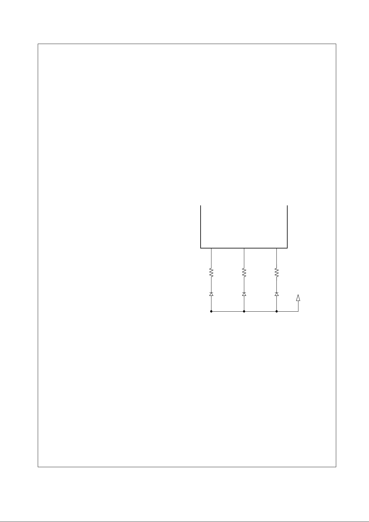
The DP83815 LED pins are capable of 6 mA. Connection
of these LED pins should ensure this is not overloaded.
Using 2 mA LED devices the connection for the LEDs
could be as shown in Figure 3-5.
Figure 3-5 LED Loading Example
V
DD
LED10N
453 Ω
LEDACTN
453 Ω
LED100N
453 Ω

3.0 Functional Description (Continued)
20 www.national.com
DP83815
3.6 Half Duplex vs. Full Duplex
The DP83815 supports both half and full duplex operation
at both 10 Mb/s and 100 Mb/s speeds.
Half-duplex is the standard, traditional mode of operation
which relies on the CSMA/CD protocol to handle collisions
and network access. In Hal f-Duplex mode, CRS res ponds
to both transmit and receive activity in order to maintain
compliance with IEEE 802.3 specification .
Since the DP83815 is designed to support simultaneous
transmit and receiv e act ivi ty it is capabl e of su ppor ting full duplex switched ap plications with a thro ug hpu t of up to 200
Mb/s per port when operating in 100BASE-TX mode.
Because the CSMA/CD protocol does not apply to fullduplex operation, the DP83815 disables its own internal
collision sensing and reporting functions.
It is important to un ders tand that while f ull Aut o-Neg oti atio n
with the use of Fast Link Pulse code words can interpret
and configure to support full-duplex, parallel detection can
not recogni ze the difference between full and half-duplex
from a fixed 10 Mb/s or 100 Mb/s link partner over twisted
pair. Therefore, as specified in 802.3u, if a far-end link
partner is transmitting forced full duplex 100BASE-TX for
example, the parallel detection state machine in the
receiving station would be unable to detect the full duplex
capability of the fa r -e nd li nk par tne r an d wou ld ne go ti at e to
a half duplex 100BASE-TX configuration (same scenario
for 10 Mb/s).
For full duplex operation, the following register bits must
also be set:
— TXCFG:CSI (Carrier Sense Ignore)
— TXCFG:HBI (HeartBeat Ignore)
— RXCFG:ATX (Accept Transmit Packets)
Additionally, the Auto-Negotiation Select bits in the
Configuration register must show full duplex support:
— CFG:ANEG_SEL
3.7 Phy Loopback
The DP83815 includes a Phy Loopback Test mode for
easy board diagnostics. The Loopback mode is selected
through bit 14 (Loopback) of the Basic Mode Control
Register (BMCR). Writi ng 1 to this bi t enable s transm it dat a
to be routed to the receive path early in the physical layer
cell. Loopback status may be checked in bit 3 of the PHY
Status Register (C0h). While in Loopback mode the data
will not be trans m itte d o nto the media. This i s true f or e ith er
10 Mb/s as well as 100 Mb/s data.
In 100BASE-TX Loopback mode the data is routed through
the PCS and PMA layers into the PMD sublayer before it is
looped back. Therefore, in addition to serving as a board
diagnostic, this mode serves as qu ick fun ction al verif icatio n
of the device.
Note: A Mac Loopback can be performed via setting bit 29
(Mac Loopback) in the Tx Configuration Register.
3.8 Status Information
There are 3 pins that are available to convey status
information to the user through LEDs to indicate the speed
(10 Mb/s or 100 Mb/s) link status and receive or transmit
activity.
10 Mb/s Link is estab lishe d as a resu lt of the rec eption of at
least seven consecutive Normal Link Pulses or the
reception of a valid 10BASE-T packet. LED10N will deassert in accordance with the Link Loss Timer specified in
IEEE 802.3.
100BASE-T Link is established as a result of an input
receive amplitude compliant with TP-PMD specifications
which will result in internal generation of Signal Detect.
LED100N will assert after the internal Signal Detect has
remained asserted for a minimum of 500 µs. LED100N will
de-assert immediately following the de-assertion of the
internal Signal Detect.
Activity LED status indicates Receive or Transmit activity.
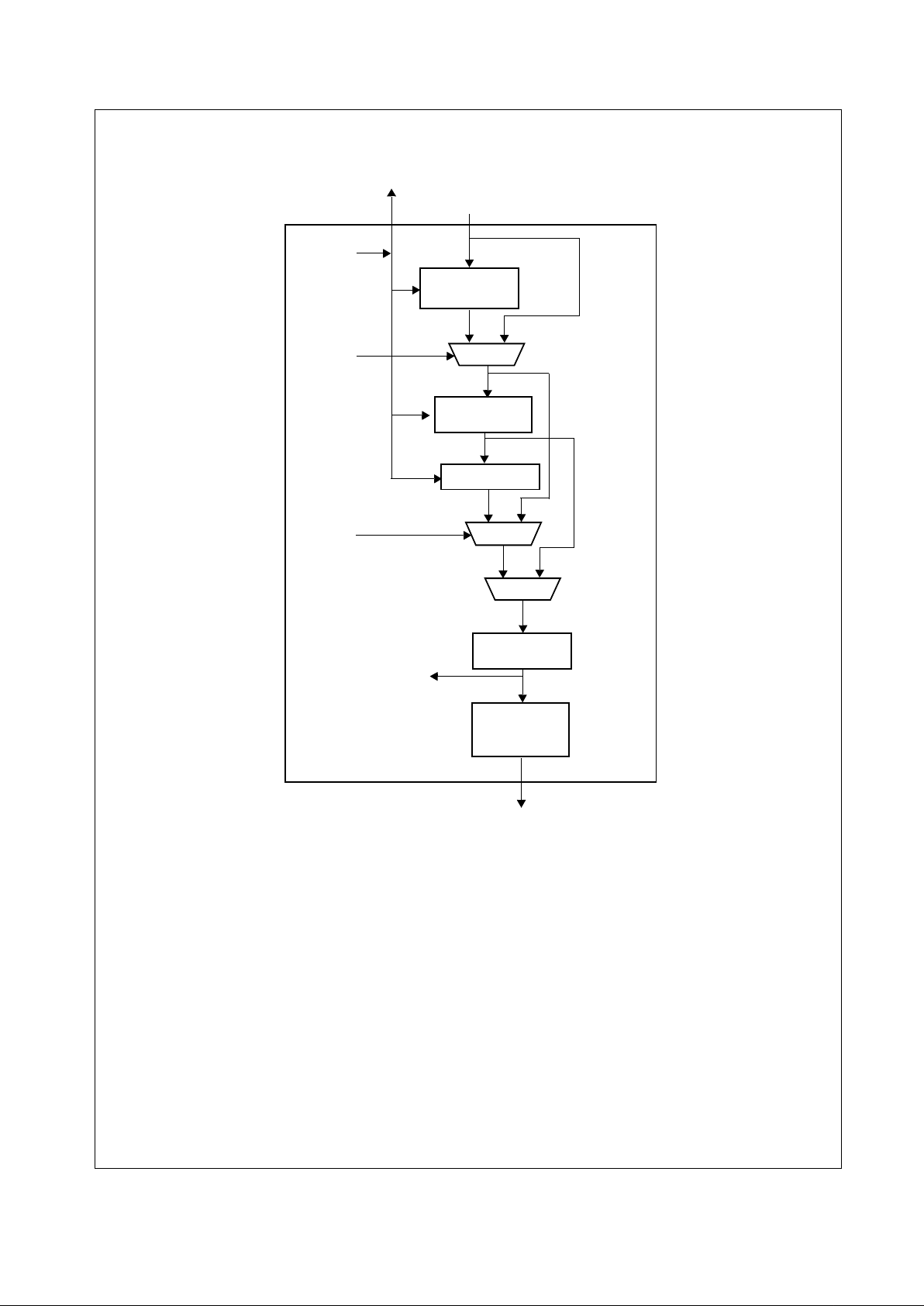
3.9 100BASE-TX TRANSMITTER
The 100BASE-TX transmitter consists of several functional
blocks which convert synchronous 4-bit nibble data, to a
scrambled MLT-3 125 Mb/s serial data stream. Because
the 100BASE-TX TP-PMD is integrated, the differential
output pins, TD±, can be directly routed to the magnetics.
The block dia gram in Figure 3-6 prov ides an overview of
each functional block within the 100BASE-TX transmit
section.
The Transmitter section consists of the following functional
blocks:
— Code-group Encode r and Injecti on block ( bypass optio n)
— Scrambler block (bypass option)
— NRZ to NRZI encoder block
— Binary to MLT-3 converter / Common Driver
The bypass option for the functional blocks within the
100BASE-TX transmitter provides flexibility for applications
such as 100 Mb/s repeaters where data conversion is not
always required. The DP83815 implements the 100BASETX transmit state machine diagram as specified in the
IEEE 802.3u Standard, Clause 24.
3.0 Functional Description (Continued)
21 www.national.com
DP83815
Figure 3-6 100BASE-TX Transmit Block Diagram
3.9.1 Code-group Encoding and Injection
The code-group encoder converts 4-bit (4B) nibble data
generated by the MAC into 5-bit (5B) code-groups for
transmission. This conversion is required to allow control
data to be combined with packet data code-groups. Refer
to Table 3-1 for 4B to 5B code-group mapping details.
The code-group encoder substitutes the first 8-bits of the
MAC preamble with a J/K code-group pair (11000 10001)
upon transmission. The code-group encoder continues to
replace subsequent 4B preamble and data nibbles with
corresponding 5B code-groups. At the end of the transmit
packet, upon the de-assertion of Transmit Enable signal
from the MAC, the code-group encoder injects the T/R
code-group pair (0 1101 00111 ) in dic at ing the en d o f fra me .
After the T/R code-group pair, the code-group encoder
continuously injects IDLEs into the transmit data stream
until the next transmit packet is detected (re-assertion of
Transmit Enable).
3.9.2 Scrambler
The scrambler is required to control the radiated emissions
at the media connector and on the twisted pair cable (for
100BASE-TX applications). By scrambling the data, the
total energy launched onto the cable is randomly
distributed over a wide frequency range. Without the
scrambler, energy levels at the PMD and on the cable
could peak beyond FCC limitations at frequencies related
to repeating 5B sequences (i.e., continuous transmission
of IDLEs).
The scrambler is configured as a closed loop linear
feedback shift register (LFSR) with an 11-bit polynomial.
The output of the closed loop LFSR is X-ORd with the
serial NRZ data from the code-group encoder. The result is
a scrambled data stream with sufficient randomization to
decrease radiated emissions at certain frequencies by as
much as 20 dB.
FROM CGM
BP_4B5B
BP_SCR
4B5B CODE-
MUX
5B PARALLEL
SCRAMBLER
MUX
MUX
NRZ TO NRZI
BINARY
TD +/-
100BASE-TX
GROUP ENABLER
TXD(3:0)/TXER
TXCLK
TO SERIAL
ENCODER
TO MLT-3/
COMMON
DRIVER
LOOPBACK
3.0 Functional Description (Continued)
22 www.national.com
DP83815
3.9.3 NRZ t o NRZI Encoder
After the transmit data stream has been serialized and
scrambled, the data must be NRZI encoded in order to
comply with the TP-PMD standard for 100BASE-TX
transmission over Category-5 un-shielded twisted pair
cable. There is no ability to bypass this block within the
DP83815.
3.9.4 Binary to MLT-3 Convertor / Common Driver
The Binary to MLT-3 conversion is accomplished by
converting the serial binary data stream output from the
NRZI encoder into two binary data streams with alternately
phased logic one events. These two binary streams are
then fed to the twisted pair output dri ve r whic h con ve rt s the
voltage to current and alternately drives either side of the
transmit transformer primary winding, res ultin g in a mini mal
current (20 mA max) MLT-3 signal. Refer to Figure 3-7
Figure 3-7 Binary to MLT-3 conversion
D
Q
Q
binary_in
binary_plus
binary_minus
binary_in
binary_plus
binary_minus
COMMON
DRIVER
MLT-3
differential MLT-3
Table 3-1 4B5B Code-Group Encoding/Decoding
Name PCS 5B Code-group Description/4B Value
DATA CODES
0 11110 0000
1 01001 0001
2 10100 0010
3 10101 0011
4 01010 0100
5 01011 0101
6 01110 0110
7 01111 0111
8 10010 1000
9 10011 1001
A 10110 1010
B 10111 1011
C 11010 1100
D 11011 1101
E 11100 1110
F 11101 1111
IDLE AND CONTROL CODES
H 00100 HALT code-group - Error code
I 11111 Inter-Packet IDLE - 0000
J 11000 First Start of Packet - 0101
K 10001 Second Start of Packet - 0101
T 01101 First End of Packet - 0000
R 00111 Second End of Packet - 0000

3.0 Functional Description (Continued)
23 www.national.com
DP83815
The 100BASE-TX MLT-3 signal sourced by the TD±
common driver output pins is slew rate controlled. This
should be considered when selecting AC coupling
magnetics to ensure TP-PMD Standard compliant
transition times (3 ns < Tr < 5 ns).
The 100BASE-TX transmit TP-PMD function within the
DP83815 is capab le o f sour cing only M LT-3 encoded data.
Binary output from the TD± outputs is not po ssible in 100
Mb/s mode.
3.10 100BASE-TX Receiver
The 100BASE-TX receiver consists of several functional
blocks which convert the scrambled MLT-3 125 Mb/s serial
data stream to synchronous 4-bit nibble data that is
provided to the MAC. Because the 100BASE-TX TP-PMD
is integrated, the differential input pins, RD±, can be
directly routed from the AC coupling magnetics.
See Figure 3-8 for a block diagram of the 100BASE-TX
receive function. This provides an overview of each
functional block within the 100BASE-TX receive section.
The Receive section consists of the following functional
blocks:
—ADC
— Input and BLW Compensation
— Signal Detect
— Digital Adaptive Equalization
— MLT-3 to Binary Decoder
— Clock Recovery Module
— NRZI to NRZ Decoder
— Serial to Parallel
— De-scrambler (bypass option)
— Code Group Alignment
— 4B/5B Decoder (bypass option)
— Link Integrity Monitor
— Bad SSD Detection
The bypass option for the functional blocks within the
100BASE-TX receiver provides flexibility for applications
such as 100 Mb/s repeaters where data conversion is not
always required.
3.10.1 Input and Base Line Wander Compensation
Unlike the DP83223V Twister, the DP83815 requires no
external attenuation circuitry at its receive inputs, RD+/−. It
accepts TP-PMD compliant waveforms directly, requiring
only a 100Ω termination plus a simple 1:1 transformer.
The DP83815 is completely ANSI TP-PMD compliant and
includes Base Line Wander (BLW) compensation. The
BLW compensation block can successfully recover the TPPMD defined “killer” pattern and pass it to the digital
adaptive equalization block.
BLW can generally be defined as the change in the
average DC content, over time, of an AC coupled digital
transmission over a given transmission medium. (i.e.
copper wire).
BLW results from the interaction between the low
frequency components of a transmitted bit stream and the
frequency response of the AC coupling component(s)
within the transmission system. If the low frequency
content of the digital bit stream goes below the low
frequency pole of the AC coupling transformers then the
droop characteristics of the transformers will dominate
resulting in potentially serious BLW.
The digital oscilloscope plot provided in Figure3-9
illustrates the severity of the BLW event that can
theoretically be generated during 100BASE-TX packet
transmission. This event consists of approximately 800 mV
of DC offset for a period of 120 us. Left uncompensated,
events such as this can cause packet loss.
3.10.2 Signal Detect
The signal detect function of the DP83815 is incorporated
to meet the specifications mandated by the A NS I FDD I TPPMD Standard as well as the IEEE 802.3 100BASE-TX
Standard for both voltage thresholds and timing
parameters.
Note that the reception of normal 10BASE-T link pulses
and fast link pulses per IEEE 802.3u Auto-Negotiation by
the 100BASE-TX receiver do not cause the DP83815 to
assert signal detect.
INVALID CODES
V 00000
V 00001
V 00010
V 00011
V 00101
V 00110
V 01000
V 01100
V 10000
V 11001
Table 3-1 4B5B Code-Group Encoding/Decoding
Name PCS 5B Code-group Description/4B Value
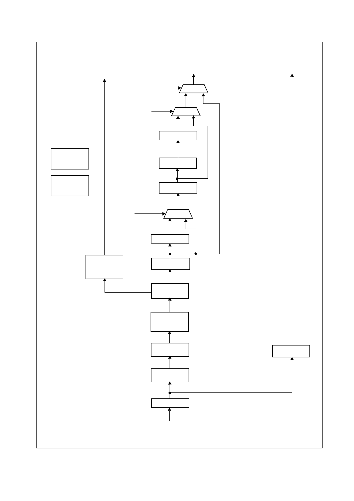
3.0 Functional Description (Continued)
24 www.national.com
DP83815
Figure 3-8 100 M/bs Receive Block Diagram
BP_4B5B
BP_SCR
BP_RX
CLOCK
MUX
MUX
4B/5B DECODER
SERIAL TO
CODE GROUP
MUX
DESCRAMBLER
NRZI TO NRZ
MLT-3 TO BINARY
DIGITAL
CLOCK
LINK INTEGRITY
RX_DATA VALID
AGC
INPUT BLW
ADC
SIGNAL
COMPENSATION
ADAPTIVE
EQUALIZATION
DECODER
DECODER
ALIGNMENT
RECOVERY
MODULE
PARALLEL
MONITOR
SSD DETECT
RXCLK
SD
RXD(3:0)/RXER
RD +/-
DETECT
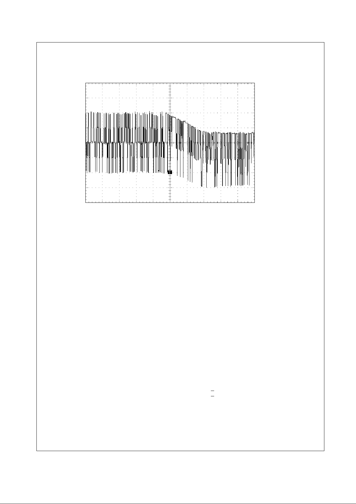
3.0 Functional Description (Continued)
25 www.national.com
DP83815
3.10.3 Digital Adaptive Equalization
When transmitting data at high speeds over copper twisted
pair cable, frequency dependent attenuation becomes a
concern. In high-speed twisted pair signalling, the
frequency content of the trans mitted signal can va ry greatl y
during normal operation based primarily on the
randomness of the scrambled data stream. This variation
in signal attenuation caused by frequency variations must
be compensated for to ensure the integrity of the
transmission.
In order to ensure quality transmission when employing
MLT-3 encoding, the co mpensation mus t be able to adapt
to various cable lengths and cable types depending on the
installed env ironment. The se lection of long cable lengths
for a given implementation, requires significant
compensation which will over-compensate for shorter, less
attenuating lengths. Conversely, the selection of short or
intermediate cable lengths requiring less compensation will
cause serious under-compensation for longer length
cables. Therefore, the compensation or equalization must
be adaptive to en sure proper condi tioning of the recei ved
signal independent of the cable length.
The DP83815 utilizes an extremely robust equalization
scheme referred to herein as ‘Digital Adaptive
Equalization’. Traditional designs use a pseudo adaptive
equalization scheme that determines the approximate
cable length by monitoring signal attenuation at certain
frequencies. This attenuation value was compared to the
internal receive input reference voltage. This comparison
would indicate the amount of equalization to use. Although
this scheme is used successfully on the DP83223V twister,
it is sensitive to transformer mismatch, resistor variation
and process induced offset. The DP83223V also required
an external attenua tio n network to help ma tch the incoming
signal amplitude to the internal reference.
The Digital Equalizer removes ISI (Inter Symbol
Interference) from the receive data stream by continuously
adapting to provide a filter with the inverse frequency
response of the channel. When used in conjunction with a
gain stage, this enables the receive 'eye pattern' to be
opened sufficiently to allow very reliable data recovery.
Traditionally 'adaptive' equalizers selected 1 of N filters in
an attempt to match the cables characteristics. This
approach will typically leave holes at certain cable lengths,
where the performance of the equalizer is not optimized.
The DP83815 equalizer is truly adaptive.
The curves given in Figure 3-10 illustrate attenuation at
certain frequencies for given cable lengths. This is derived
from the worst case frequency vs. attenuation figures as
specified in the EIA/TIA Bulletin TSB-36. These curves
indicate the significant variations in signal attenuation that
must be compensated for by the receive adaptive
equalization circuit.
Figure 3-11 represents a scrambled IDLE transmitted over
zero meters of cable as measured at the AII (Active Input
Interface) of the receiver. Figure 3-12 and Figure 3-13
represent the signal degradation over 50 and 100 meters
of category V
cable respectively, also measured at the AII.
These plots show the extreme degradation of signal
integrity and indicate the requirement for a robust adaptive
equalizer.
Figure 3-9 100BASE-TX BLW Event Diagram
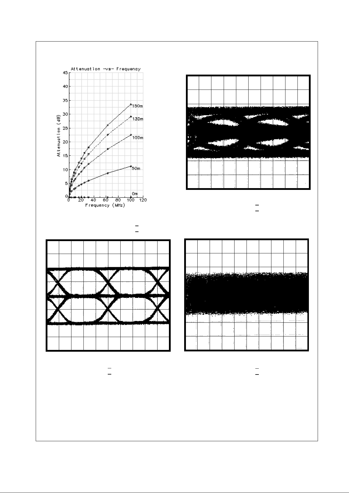
3.0 Functional Description (Continued)
26 www.national.com
DP83815
3.10.4 Line Quality Monitor
It is possible to determine the amount of Equalization being
used by accessing certain test registers with the DSP
engine. This provides a crude indication of connected
cable length. This function allows for a quick and simple
verification of the line quality in that any significant
deviation from an expected register value (based on a
known cable length) would indicate that the signal quality
has deviated from the expected nominal case.
3.10.5 MLT-3 to NRZI Decoder
The DP83815 decodes the MLT-3 information from the
Digital Adaptive Equalizer block to binary NRZI data.
Figure 3-10 EIA/TIA Attenuation vs. Frequenc y for 0, 50,
100, 130 & 150 meters of CAT V
cable
Figure 3-11 MLT-3 Signal Measured at AII after 0 meters
of CAT V
cable
2ns/div
Figure 3-12 MLT-3 Signal Measured at AII after 50
meters of CAT V
cable
Figure 3-13 MLT-3 Signal Measured at AII after 100
meters of CAT V cable
2ns/div
2ns/div

3.0 Functional Description (Continued)
27 www.national.com
DP83815
3.10.6 Clock Recovery Module
The Clock Recovery Module (CRM) accepts 125 Mb/s
MLT3 data from the equalizer. The DPLL locks onto the
125 Mb/s data str eam and extracts a 125 MHz recover ed
clock. The extracted and synchronized clock and data are
used as required by the synchronous re ce iv e o per atio ns a s
generally depicted in Figure3-8.
The CRM is implemented using an advanced all digital
Phase Locked Loop (PLL) architecture that replaces
sensitive analog circuitry. Using digital PLL circuitry allows
the DP83815 to be manufactured and specified to tighter
tolerances.
3.10.7 NRZI to NRZ
In a typical application, the NRZI to NRZ decoder is
required in order to present NRZ formatted data to the descrambler (or to the code-group alignment block, if the descrambler is bypassed, or directly to the PCS, if the
receiver is bypassed).
3.10.8 Serial to Parallel
The 100BASE-TX receiver includes a Serial to Parallel
converter which supplies 5-bit wide data symbols to the
PCS Rx state machine.
3.10.9 De-scrambler
A serial de-scrambler is used to de-scramble the received
NRZ data. The de-scrambler has to generate an identical
data scrambling sequence (N) in order to recover the
original unscrambled data (UD) from the scrambled data
(SD) as represented in the equations:
Synchronization of the de-scrambler to the original
scrambling sequence (N) is achieved based on the
knowledge that the incoming scrambled data stream
consists of scrambled IDLE data. After the de-scrambler
has recognized 12 consecutive IDLE code-groups, where
an unscrambled IDLE code-group in 5B NRZ is equal to
five consecutive ones (11111), it will synchronize to the
receive data stream and generate unscrambled data in the
form of unaligned 5B code-groups.
In order to maintain synchronization, the de-scrambler
must continuo usly monitor the va lidity of the uns crambled
data that it generates. To ensure this, a line state monitor
and a hold timer are used to constantly monitor the
synchronization status. Upon synchronization of the descrambler the hold timer starts a 722 µs countdown. Upon
detection of sufficient IDLE code-groups (58 bit times)
within the 722 µs period, the hold timer will reset and begin
a new countdown . This monitoring op eration will cont inue
indefinitely given a properly operating network connection
with good signal integrity. If the line state monitor does not
recognize sufficient unscrambled IDLE code-groups within
the 722 µs period, the entire de-scrambler will be forced
out of the current state of synchronization and reset in
order to re-acquire synchronization.
3.10.10 Code-group Alignment
The code-group alignment module operates on unaligned
5-bit data f rom th e de-sc rambler (or, if the de -scram bler is
bypassed, directly from the NRZI/NRZ decoder) and
converts it into 5B code-group data (5 bits). Code-group
alignment occurs after the J/K code-group pair is detected.
Once the J/K code-group pair (11000 10001) is detected,
subsequent data is aligned on a fixed boundary.
3.10.11 4B/5B Decoder
The code-group decoder functions as a look up table that
translates incoming 5B code-groups into 4B nibbles. The
code-group decoder first detects the J/K code-group pair
preceded by IDLE code-groups and replaces the J/K with
MAC preamble. Spec ific all y, the J/K 10-bit code- grou p pair
is replaced by the nibble pair (0101 0101). All subsequent
5B code-groups are converted to the corresponding 4B
nibbles for the duration of the entire packet. This
conversion ceases upon the detection of the T/R codegroup pair denoting the End of Stream Delimiter (ESD) or
with the reception of a minimum of two IDLE code-groups.
3.10.12 100BASE-TX Link Integrity Monitor
The 100 Base-TX Link monitor ensures that a valid and
stable link is established before enabling both the Transmit
and Receive PCS layer.
Signal detect must be valid for 395 µs to allow the link
monitor to enter the 'Link Up' state, an d e nab le the transmit
and receive functions.
Signal detect can be forced active by setting Bit 1 of the
PCSR.
Signal detect can be optionally ANDed with the descrambler locked indication by setting bit 8 of the PCSR.
When this option is enabled, then De-scrambler 'locked' is
required to enter the Link Up sta te, but only Signal det ect is
required to maintain the link in the link Up state.
3.10.13 Bad SSD Detection
A Bad Start of Stream Delimiter (Bad SSD) is any transition
from consecutive idle code-groups to non-idle code-groups
which is not prefixed by the code-group pair J/K.
If this condition is detected, the DP83815 will assert RXER
and present RXD[3 :0] = 1110 to the M AC fo r th e cy cl es th at
correspond to received 5B code-groups until at least two
IDLE code groups are detected. In addition, the False
Carrier Event Counter will be incremented by one.
Once at least two IDLE c ode gro up s a r e de tect ed , th e e rror
is reported to the MAC.
UD SD N⊕()=
SD UD N⊕()=
3.0 Functional Description (Continued)
28 www.national.com
DP83815
3.11 10BASE-T Transceiver Module
The 10BASE-T Transceiver Module is IEEE 802.3
compliant. It includes the receiver, transmitter, collision,
heartbeat, loopback, jabber, and link integrity functions, as
defined in the standard. An external filter is not required on
the 10BASE-T interface since this is integrated inside the
DP83815. This section focuses on the general 10BASE-T
system level operation.
3.11.1 Operational Modes
The DP83815 has two basic 10BASE-T operational
modes:
— Half Duplex mode - functions a s a s tan dard IEEE 802 .3
10BASE-T transceiver supporting the CSMA/CD
protocol.
— Full Duplex mode - capable of simultaneously
transmitting and receiving without reporting a collision.
The DP83815's 10 Mb/s ENDE C is des ign ed to enco de
and decode simultaneously.
3.11.2 Smart Squelch
The smart squelch is responsible for determining when
valid data is present on the differential receive inputs
(RD±). The DP83815 implements an intelligent receive
squelch to ensure that impulse noise on the receive inputs
will not be mistaken for a valid signal. Smart squelch
operation is independent of the 10BASE-T operational
mode.
The squelch circuitry employs a combination of amplitude
and timing measurements (as specified in the IEEE 802.3
10BASE-T standard) to determine the validity of data on
the twisted pair inputs (refer to Figure 3-14).
The signal at the start of packet is checked by the smart
squelch and any pulses not exceeding the squelch level
(either positive or negative, depending upon polarity) will
be rejected. Once this first squelch level is overcome
correctly, the opposite squelch level must then be
exceeded within 150 ns. Finally the signal must again
exceed the original squelch level within a 150 ns to ensure
that the input waveform will not be rejected. This checking
procedure result s in the l oss of typic ally t hree preamb le bit s
at the beginning of each packet.
Only after all these conditions have been satisfied will a
control signal be generated to indicate to the remainder of
the circuitry that valid data is present. At this time, the
smart squelch circuitry is reset.
Valid data is considered to be present until the squelch
level has not been g enerated for a time long er th an 150 ns ,
indicating the End of Packet. Once good data has been
detected the squelch levels are reduced to minimize the
effect of noise causing premature End of Packet detection.
3.11.3 Collision Detection
When in Half Duplex, a 10BASE-T collision is detected
when the receive and transmit channels are active
simultaneously. Collisions are reported to the MAC.
Collisions are also reported when a jabber condition is
detected.
If the ENDEC is receiving when a collision is detected it is
reported immediately (through the COL signal).
When heartbeat is enabled, approximately 1 µs after the
transmission of each packet, a Signal Quality Error (SQE)
signal of approximate ly 10 bit tim es is generate d to indi cate
successful transmission.
The SQE test is inhibited when the physical layer is set in
full duplex mode. SQE can also be inhibited by setting the
HEARTBEAT_DIS bit in the TBTSCR register.
3.11.4 Normal Link Pulse Detection/Generation
The link pulse generator produces pulses as defined in the
IEEE 802.3 10BASE-T standard. Each link pulse is
nominally 100 ns in duration and transmitted every 16 ms
in the absence of transmit data.
Link pulses are used to check the integrity of the
connection with the remote end. If valid link pulses are not
received, the link detector disables the 10BASE-T twisted
pair transmitter, receiver and collision detection functions.
When the link integrity function is disabled
(FORCE_LINK_10 of the TBTSCR register), good link is
forced and the 10BASE-T transceiver will operate
regardless of the presence of link pulses.
Figure 3-14 10BASE-T Twisted Pair Smart Squelch Operation
end of packet
start of packet
V
SQ-(reduced)
V
SQ-
V
SQ+(reduced)
V
SQ+
<150 ns
<150 ns
>150 ns

3.0 Functional Description (Continued)
29 www.national.com
DP83815
3.11.5 Jabber Function
The jabber function monitors the DP83815's output and
disables the transmitte r if it att empts to transmit a packet of
longer than legal size. A jabber timer monitors the
transmitter and disables the transmission if the transmitter
is active for approximately 20-30 ms.
Once disabled by the jabber function, the transmitter stays
disabled for the entire time that the ENDEC module's
internal transmit enable is asserted. This signal has to be
de-asserted for approximately 400-600 ms (the “unjab”
time) before the jabber function re-enables the transmit
outputs.
The Jabber function is only me aningf ul in 10 BASE-T mod e.
3.11.6 Automatic Link Polarity Detection
The DP83815's 10BASE-T transceiver module
incorporates an automatic link polarity detection circuit.
When seven consecutive li nk pulses or t hree consec utive
receive packets with inverted End-of-Packet pulses are
received, bad polarity is reported .
A polarity reversal can be cau sed by a wiring error a t either
end of the cable, usually at the Main Distribution Frame
(MDF) or patc h panel in the wiring closet.
The bad polarity condition is latched. The DP83815's
10BASE-T transceiver module corrects for this error
internally and will continue to decode received data
correctly. This eliminates the need to correct the wiring
error immediately.
3.11.7 10BASE-T Internal Loopback
When the LOOPBACK bit in the BMCR register is set,
10BASE-T transmit data is looped back in the ENDEC to
the receive channel. The transmit drivers and receive input
circuitry are disabled in transceiver loopback mode,
isolating the transceiver from the network.
Loopback is used for diagnostic testing of the data path
through the transceiver without transmitting on the network
or being interrupted by receive traffic. This loopback
function causes the data to loopback just prior to the
10BASE-T output driver buffers such that the entire
transceiver path is tested.
3.11.8 Transmit and Receive Filtering
External 10BASE-T filters are not required when using the
DP83815, as the required signal conditioning is integrated
into the device.
Only isolation/step-up transformers and impedance
matching resistors are required for the 10BASE-T transmit
and receive interface. The internal transmit filtering
ensures that all the harmonics in the transmit signal are
attenuated by at least 30 dB.
3.11.9 Transmitter
The encoder begins operation when the transmit enable
input to the physical layer is asserted and converts NRZ
data to pre-emphasized Manchester data for the
transceiver. For the duration of assertion, the serialized
transmit data is encoded for the transmit-driver pair (TD±).
The last transition is always positive; it occurs at the center
of the bit cell if the last bit is a one, or at the end of the bit
cell if the last bit is a zero.
3.11.10 Receiver
The decoder consist s of a di fferential receiver and a PLL to
separate a Manchester encoded data stream into internal
clock signals and data. The differential input must be
externally terminated with a differential 100Ω termination
network to accommodate UTP cable. The internal
impedance of RD± (typically 1.1Kohms) is in parallel with
two 54.9 resistors to approximate the 100Ω termination.
The decoder detect s the end of a fra me whe n no m ore mi dbit transitions are detected.
3.11.11 Far End Fault Indication
Auto-Negotiation provides a mechanism for transferring
information from the Loca l Station to the Link Partner that a
remote fault has occurred for 100BASE-TX.
A remote fault is an error in the link that one station can
detect while the other cannot. An example of this is a
disconnected fiber a t a st a tion’ s tra nsmi tter. This station will
be receiving valid data and detect that the link is good via
the Link Integrity Monitor, but will not be able to detect that
its transmission is not pr opagating to the other station.
If three or more FEFI IDLE patterns are detected by the
DP83815, then bit 4 of the Basic Mode Status register is
set to one until read by management, additionally bit 7 of
the PHY Status register is also set.
The first FEFI IDLE pattern may co nt ain mo re than 84 one s
as the pattern may have started during a normal IDLE
transmission which is actually quite likely to occur.
However, since FEFI is a repeating pattern, this will not
cause a problem with the FEFI function. It should be noted
that receipt of the FEFI IDLE pattern will not cause a
Carrier Sense error to be reported.
If the FEFI function has been disabled via FEFI_EN (bit 3)
of the PCSR Configuration register, then the DP83815 will
not send the FEFI IDLE pattern.
3.12 802.3u MII
The DP83815 incorporates the Media Independent
Interface (MII) as specifi ed in Claus e 22 of the IEEE 80 2.3u
standard. This interface may be used to connect PHY
devices. This section describes the MII configuration steps
as well as the serial MII management interface and nibble
wide MII data interface.
3.12.1 MII Access Configuration
The DP83815 must be specifically configured for
accessing the MII. This is done by first connecting pin 133
(MD1/CFGDISN) to GND through a 1KΩ resistor. Then
setting bit 12 (EXT_PHY) of the CFG regi ster (offset 04h)
to 1. See Section 4.2.2. When this bit is set, the internal
Phy is automatically disabled, as reported by bit 9
(PHY_DIS) of the CFG reg ister. The MII must then be reset
before the external PHY can be detected.
If external MII is not selected as described then the internal
Phy is used and the MII pins of the MacPhyter can be left
unconnected.
3.12.2 MII Serial Management
The MII serial management interface allows for the
configuration and control of PHY registers, gathering of
status, error information, and the determination of the type
and capabilities of the attached PHY(s).
The MII serial management specification defines a set of
thirty-two 16-bit status and control registers that are
accessible through the management interface pins MDC
and MDIO. A description of the serial management
interface access and access protocol follows.
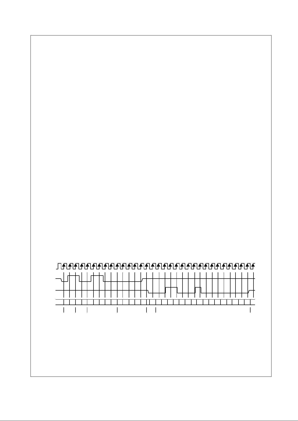
3.0 Functional Description (Continued)
30 www.national.com
DP83815
3.12.3 MII Serial Management Access
Management access to the PHY(s) is done via
Management Data Clock (MDC) and Management Data
Input/Output (MDIO). M DC ha s a m aximum cloc k rate of 25
MHz and no minimum rate. The MDIO line is bi-directional
and may be shared by up to 32 devices. The internal PHY
counts as one of these 32 devices.
The internal PHY has the advantage of having direct
register access but can also be controlled exactly like a
PHY, with a default address of 1Fh, connected to the MII.
Access and control of the MDC and MDIO pins is done via
the MII/EEPROM Access Register (MEAR). The clock
(MDC) is created by alternating writes of 0 then 1 to the
MDC bit (bit 6). Control of data direction is done by the
MDDIR bit (bit 5). Data is either recorded or written by the
MDIO bit (bit 4). Setting the MDDIR bit to a 1 allows the
DP83815 to drive the MDIO pin. Setting the MDDIR bit to a
0 allows the MDIO bit to reflect the value of the MDIO pin.
See Section 4 .2.3
This bit-bang access of the MDC and MDIO pins thus
requires 64 accesses to the MEAR register to complete a
single PHY register transaction. Since a PHY device is
typically self configuring and adaptive this serial
management access is usually only required at
initialization time and therefore is not time critical.
3.12.4 Serial Management Access Protocol
The serial control interface clock (MDC) has a maximum
clock rate of 25 MHz and no minimum rate. The MDIO line
is bi-directional and may be shared by up to 32 devices.
The MDIO frame format is shown in Table 3-2.
If external PHY devices may be attached and removed
from the MII there should be a 15 KΩ pull-down resistor on
the MDIO signal. If the PHY will always be connected then
there should be a 1.5 kΩ pull-up resistor which, during
IDLE and turnaround, will pull MDIO high. In order to
initialize the MDIO interface, the DP83815 sends a
sequence of 32 contiguous logic ones on MDIO provides
the PHY(s) with a sequence that can be used to establish
synchronization. This preamble may be generated either
by driving MDIO high for 32 consecutive MDC clock c yc les,
or by simply allowing the MDIO pull-up resistor to pull the
MDIO pin high du ring which ti me 32 MDC cl ock cycle s ar e
provided. In addition 32 MDC clock cycles should be used
to re-sync the device if an invalid start, opcode, or
turnaround bit is detected.
The St art c ode is in dic ate d by a <01> pattern. This assures
the MDIO line transitions from the default idle line state.
Turnaround is defined as an idle bit time inserted between
the Register Address field and the Data field. To avoid
contention during a read transaction, no device shall
actively drive the MDIO signal during the first bit of
Turnaround. The addressed PHY drives the MDIO with a
zero for the second bit of turnaround and follows this with
the required data. Figure 3-15 shows the timing
relationship between MDC and the MDIO as
driven/received by the DP83815 and a PHY for a typical
register read access.
For write transactions, the DP83815 writes data to the
addressed PHY thus eliminating the requirement for MDIO
Turnaround. The Turnaround time is filled by the DP83815
by inserting <10>. Figure 3-16 shows the timing
relations hip for a typical MII register write access.
3.12.5 Nibble-wide MII Data Interface
Clause 22 of the IEEE 802.3u specification defines the
Media Independent Interface. This interface include
separate dedicated receive and transmit busses. These
two data buses, along with various control and indication
signals, allow for the simultaneous exchange of data
between the DP83815 and PHY(s).
Table 3-2 Typical MDIO Frame Format
MII Management
Serial Protocol
<idle><start><op code><device addr><reg addr><turnaround><data><idle>
Read Operation <idle><01><10><AAAAA><RRRRR><Z0><xxxx xxxx xxxx xxxx><idle>
Write Operation <idle><01><01><AAAAA><RRRRR><10><xxxx xxxx xxxx xxxx><idle>
Figure 3-15 Typical MDC/MDIO Read Operation
MDC
MDIO
00011 110000000
(STA)
Idle Start
Opcode
(Read)
PHY Address
(PHYAD = 0Ch)
Register Address
(00h = BMCR)
TA
Register Data
Z
MDIO
(PHY)
Z
Z
Z
0 0 011000100000000
Z
Idle
Z
Z

3.0 Functional Description (Continued)
31 www.national.com
DP83815
The receive interface consists of a nibble wide data bus
RXD[3:0], a receiv e e rror s ig nal RXER, a receive data valid
flag RXDV, and a receive clock RXCLK for synchronous
transfer of the data. The receive clock can operate at 2.5
MHz to support 10 Mb/s operation modes or at 25 MHz to
support 100 Mb/s operational modes.
The transmit interface consists of a nibble wide data bus
TXD[3:0], a transmit enable control signal TXEN, and a
transmit clock TXCLK which runs at 2.5 MHz or 25 MHz.
Additionally, the MII includes the carrier sense signal CRS,
as well as a collision detect signal COL. The CRS signal
asserts to ind icate the re ception of d ata from the ne twork
or as a function of transmit data in Half Duplex mode. The
COL signal asse rt s as an ind ic atio n of a collision which can
occur during half-duplex operation when both a transmit
and receive operation occur simultaneously.
3.12.6 Collision Detection
For Half Duplex, a 10BASE-T or 100BASE-TX collision is
detected when the receive and transmit channels are
active simu ltaneously. Collisions are reported by the COL
signal on the MII.
If the PHY is transmitting in 10 Mb/s mode when a collision
is detected, the collision is not reported until seven bits
have been received while in the collision state. This
prevents a collision being reported incorrectly due to noise
on the network. The COL signal remains set for the
duration of the collision.
If a collision occurs during a receive operation, it is
immediately reported by the COL signal.
When heartbeat is enabled (only applicable to 10 Mb/s
operation), approximately 1µs after the transmission of
each packet, a Signal Quality Error (SQE) signal of
approximately 10 bit times is generated (internally) to
indicate successful transmission. SQE is reported as a
pulse on the COL signal of the MII.
3.12.7 Carrier Sense
Carrier Sense (CRS) is asserted due to receive activity,
once valid data is detected, during 10 Mb/s operation.
During 100 Mb/s operation CRS is asserted when a valid
link (SD) and two non-contiguous zeros are detected.
For 10 or 100 Mb/s Half Duple x op era tio n, C RS is a sserte d
during either packet transmission or reception.
For 10 or 100 Mb/s Full Duplex operation, CRS is asserted
only due to receive activity.
CRS is de-asserted following an end of packet.
Figure 3-16 Typical MDC/MDIO Write Operation
MDC
MDIO
00011110000000
(STA)
Idle Start
Opcode
(Write)
PHY Address
(PHYAD = 0Ch)
Register Address
(00h = BMCR)
TA
Register Data
Z
0 0 0 000 00000000
Z
Idle
1000
ZZ

32 www.national.com
DP83815
4.0 Register Set
4.1 Configuration Registers
The DP83815 implements a PCI version 2.2 configuration register spac e. This allows a PCI BIOS to "soft" configure the
DP83815. Software Res et h as no e f f ect on configuration registers. Hardware Reset returns all configuration registers to
their hardware reset state. For all unused registers, writes are ignored, and reads return 0.
Table 4-1 Configuration Register Map
4.1.1 Configuration Identification Register
This register identifies the DP83815 Controller to PCI system software.
Offset Tag Description Access
00h CFGID Configuration Identification Register RO
04h CFGCS Configuration Command and Status Register R/W
08h CFGRID Configuration Revision ID Register RO
0Ch CFGLAT Configuration Latency Timer Register RO
10h CFGIOA Configuration IO Base Address Register R/W
14h CFGMA Configuration Memory Address Register R/W
18h-28h Reserved (reads return zero)
2Ch CFGSID Configuration Subsystem Identification Register RO
30h CFGROM Boot ROM configuration register R/W
34h CAPPTR Capabilities Pointer Register RO
38h Reserved (reads return zero)
3Ch CFGINT Configuration Interrupt Select Register R/W
40h PMCAP Power Management Capabilities Register RO
44h PMCSR Power Management Control and Status Register R/W
48-FFh Reserved (reads return zero)
Tag: CFGID Size: 32 bits Hard Reset: 0020100Bh
Offset: 00h Access: Read Only Soft Reset: Unchanged
Bit Bit Name Description
31-16 DEVID Device ID
This field is read-only and is set to the device ID assigned by National Semiconductor to the DP83815,
which is 0020h.
15-0 VENID Vendor ID
This field is read-only and is set to a value of 100Bh which is National Semiconductor's PCI Vendor ID.

33 www.national.com
4.0 Register Set (Continued)
DP83815
4.1.2 Configuration Command and Status Register
The CFGCS register has tw o p arts . The up per 16-bi ts (31-16) a re devo ted to de vice sta tus. A s tatu s bit is re set when ever
the register is written, and th e correspo nding bit loc ation i s a 1. The lower 16-bits (15-0) are devot ed t o comman d and a re
used to configure and control the device.
Tag: CFGCS Size: 32 bits Hard Reset: 02900000h
Offset: 04h Access: Read Write Soft Reset: Unchanged
Bit Bit Name Description
31 DPERR Detected Parity Error
Refer to the description in the PCI V2.2 specification.
30 SSERR Signaled SERR
Refer to the description in the PCI V2.2 specification.
29 RMABT Received Master Abort
Refer to the description in the PCI V2.2 specification.
28 RTABT Received Target Abort
Refer to the description in the PCI V2.2 specification.
27 STABT Sent Target Abort
Refer to the description in the PCI V2.2 specification.
26-25 DSTIM DEVSELN Timing
This field will always be set to 01 indicating that DP83815 supports “medium” DEVSELN timing.
24 DPD Data Parity Detected
Refer to the description in the PCI V2.2 specification.
23 FBB Fast Back-to-Back Capable
DP83815 will set this bit to 1.
22-21 unused
(reads return 0)
20 NCPEN New Capabilities Enable
When set, this bit indicates that the Capabilities Pointer contains a valid value and new capabilities such
as power management are supported. When clear, new capabilities (CAPPTR, PMCAP, PMCS) are
disabled. The value in this register will either be loaded from the EEPROM or, if the EEPROM is
disabled, from a strap option at reset.
19-16 Unused
(reads return 0)
15-10 Unused
(reads return 0)
9 FBBEN Fast Back-to-Back Enable
Set to 1 by the PCI BIOS to enable the DP83815 to do Fast Back-to-Back transfers (FBB transfers as a
master is not implemented in the current revision).
8 SERREN SERRN Enable
When SERREN and PERRSP are set, DP83815 will generate SERRN during target cycles when an
address parity error is detected from the system. Also, when SERREN and PERRSP are set and
CFG:PESEL is reset, master cycles detecting data parity errors will generate SERRN.
7 Unused
(reads return 0)

34 www.national.com
4.0 Register Set (Continued)
DP83815
4.1.3 Configuration Revision ID Register
This register stores the silicon revision number, revision number of software interface specification and lets the
configuration software know that it is an Ethernet controller in the class of network controllers.
Bit Bit Name Description
6 PERRSP Parity Error Response
When set, DP83815 will assert PERRN on the detection of a data parity error when acting as the target,
and will sample PERRN when acting as the initiator. Also, setting PERRSP allows SERREN to enable
the assertion of SERRN. When reset, all address and data parity errors are ignored and neither SERRN
nor PERRN are asserted.
5-3 Unused
(reads return 0)
2 BMEN Bus Master Enable
When set, DP83815 is allowed to act as a PCI bus master. When reset, DP83815 is prohibited from
acting as a PCI bus master.
1 MSEN Memory Space Address
When set, DP83815 responds to memory space accesses. When reset, DP83815 ignores memory
space accesses.
0 I/OSEN I/O Space Access
When set, DP83815 responds to I/O space accesses. When reset, DP83815 ignores I/O space
accesses.
Tag: CFGRID Size: 32 bits Hard Reset: 02000000h
Offset: 08h Access: Read Only Soft Reset: Unchanged
Bit Bit Name Description
31-24 BASECL Base Class
Returns 02h which specifies a network controller.
23-16 SUBCL Sub Class
Returns 00h which specifies an Ethernet controller.
15-8 PROGIF Programming IF
Returns 00h which specifies the first release of the DP83815 Software Interface Specification.
7-0 REVID Silicon Revision
Returns 00h which specifies the silicon revision.

35 www.national.com
4.0 Register Set (Continued)
DP83815
4.1.4 Configuration Latency Timer Register
This register gives status and controls such miscellaneous functions as BIST, Latency timer and Cache line size.
DP83815 Bus Master Operations:
Independent of cache line size, the DP83815 will use the following PCI commands for bus mastered transfers:
0110 - Mem Read for all read cycles,
0111 - Mem Write for all write cycl es.
4.1.5 Configuration I/O Base Address Register
This register specifies the Base I/O address which is required to build an address map during configuration. It also
specifies the number of bytes required as well as an indication that it can be mapped into I/O space.
Tag: CFGLAT Size: 32 bits Hard Reset: 00000000h
Offset: 0Ch Access: Read Write Soft Reset: Unchanged
Bit Bit Name Description
31 BISTCAP BIST Capable
Reads will always return 0.
30 BISTEN BIST Enable
Reads will return a 0, writes are ignored.
29-16 Reserved
Reads will return a 0, writes are ignored.
15-8 LAT Latency Timer
Set by software to the number of PCI clocks that DP83815 may hold the PCI bus.
7-0 CLS Cache Line Size
Ignored by DP83815.
Tag: CFGIOA Size: 32 bits Hard Reset: 00000001h
Offset: 10h Access: Read Write Soft Reset: Unchanged
Bit Bit Name Description
31-8 IOBASE Base I/O Address
This is set by software to the base I/O address for the Operational Register Map.
7-2 IOSIZE Size indication
Read back as 0. This allows the PCI bridge to determine that the DP83815 requires 256 bytes of I/O
space.
1 Unused
(reads return 0).
0 IOIND I/O Space Indicator
Set to 1 by DP83815 to indicate that DP83815 is capable of being mapped into I/O space. Read Only.

36 www.national.com
4.0 Register Set (Continued)
DP83815
4.1.6 Configuration Memory Address Register
This registe r speci fi es th e Base Memor y addr es s which is required to build an address map during configuration. It also
specifies the number of bytes required as well as an indication that it can be mapped into memory space.
4.1.7 Configuration Subsystem Identification Register
The CFGSID allows system software to distinguish between different subsystems based on the same PCI silicon. The
values in this register can be loaded from the EEPROM if configuration is enabled.
Tag: CFGMA Size: 32 bits Hard Reset: 00000000h
Offset: 14h Access: Read Write Soft Reset: unchanged
Bit Bit Name Description
31-12 MEMBASE Memory Base Address
This is set by software to the base address for the Operational Register Map.
11-4 MEMSIZE Memory Size
These bits return 0, which indicates that the DP83815 requires 4096 bytes of Memory Space (the
minimum recommended allocation).
3 MEMPF Prefetchable
Set to 0 by DP83815. Read Only.
2-1 MEMLOC Location Selection
Set to 00 by DP83815. This indicates that the base register is 32-bits wide and can be placed anywhere
in the 32-bit memory space. Read Only.
0 MEMIND Memory Space Indicator
Set to 0 by DP83815 to indicate that DP83815 is capable of being mapped into memory space. Read
Only.
Tag: CFGSID Size: 32 bits Hard Reset: 00000000h
Offset: 2Ch Access: Read Only Soft Reset: unchanged
Bit Bit Name Description
31-16 SDEVID Subsystem Device ID
Set to 0 by DP83815.
15-0 SVENID Subsystem Vendor ID
Set to 0 by DP83815.

37 www.national.com
4.0 Register Set (Continued)
DP83815
4.1.8 Boot ROM Configuration Register
4.1.9 Capabilities Pointer Register
This register stores the capabilities linked list offset into the PCI configuration space.
Tag: CFGROM Size: 32 bits Hard Reset: 00000000h
Offset: 30h Access: Read Write Soft Reset: unchanged
Bit Bit Name Description
31-16 ROMBASE ROM Base Address
Set to the base address for the boot ROM.
15-11 ROMSIZE ROM Size
Set to 0 indicating a requirement for 64K bytes of Boot ROM space. Read only.
10-1 unused
(reads return 0)
0 ROMEN ROM Enable
This is used by the PCI BIOS to enable accesses to boot ROM. This allows the DP83815 to share the
address decode logic between the boot ROM and itself. The BIOS will copy the contents of the boot
ROM to system RAM before executing it. Set to 1 enables the address decode for boot ROM disabling
access to operational target registers.
Tag: CAPPTR Size: 32 bits Hard Reset: 00000040h
Offset: 34h Access: Read Only Soft Reset: unchanged
Bit Bit Name Description
31-8 unused
(reads return 0)
7-0 CLOFS Capabilities List Offset
Offset into PCI configuration space for the location of the first item in the Capabilities Linked List, set to
40h to point to the PMCAP register.

38 www.national.com
4.0 Register Set (Continued)
DP83815
4.1.10 Configuration Interrupt Select Register
This register stores the interrupt line number as identified by the POST software that is connected to the interrupt
controller as well as DP83815 desired settings for maximum latency and minimum grant. Max latency and Min latency
can be loaded from the EEPROM.
4.1.11 Power Management Capabilities Register
This register provides information on the capabilities of the functions related to power management. This register also
contains a pointe r to t he next ite m in th e cap abil ities list and th e cap abi lity ID fo r Power Manag ement. This re gister i s only
visible if CFGCS[4] is set.
Tag: CFGINT Size: 32 bits Hard Reset: 340b0100h
Offset: 3Ch Access: Read Write Soft Reset: unchanged
Bit Bit Name Description
31-24 MXLAT Maximum Latency
The DP83815 desired setting for Max Latency. The DP83815 will initiali ze this field t o 52d (13 µsec). The
value in this register can be loaded from the EEPROM.
23-16 MNGNT Minimum Grant
The DP83815 desired setting for Minimum Grant. The DP83815 will initialize this field to 11d (2.75 usec).
The value in this register can be loaded from the EEPROM.
15-8 IPIN Interrupt Pin
Read Only, always return 0000 0001 (INTA).
7-0 ILINE Interrupt Line
Set to which line on the interrupt controller that the DP83815's interrupt pin is connected to.
Tag: PMCAP Size: 32 bits Hard Reset: FF820001
Offset: 40h Access: Read Only Soft Reset: unchanged
Bit Bit Name Description
31-27 PMES PM E Su p por t
This 5 bit field indicates the power states in which DP83815 may assert PMEN. A 1 indicates PMEN
is enabled for that state, a 0 indicates PMEN is inhibited in that state.
XXXX1 - PMEN can be asserted from state D0
XXX1X - PMEN can be asserted from state D1
XX1XX - PMEN can be asserted from state D2
X1XXX - PMEN can be asserted from state D3hot
1XXXX - PMEN can be asserted from state D3cold
The DP83815 will only report PME support for D3cold if auxiliary power is detected on the 3VAUX
pin, in addition this value can be loaded from the EEPROM when in the D3cold state.
26 D2S D2 Support
This bit is set to a 1 when the DP83815 supports the D2 state.
25 D1S D1 Support
This bit is set to a 1 when the DP83815 supports the D1 state.

39 www.national.com
4.0 Register Set (Continued)
DP83815
4.1.12 Power Management Control and Status Register
This register contains PM control and status information.
Bit Bit Name Description
24-22 AUX_CURRENT Aux_Current
This 3 bit field reports the 3.3Vaux auxiliary current requirements for the PCI function.
If PMEN generation from D3cold is not supported by the function(PMCAP[31]), this field returns a
value of "000b" when read.
Bit 3.3Vaux
24 23 22
Max. Current Required
1 1 0 320 mA
0 0 0 0 (self powered)
21 DSI Device Specific Initialization
This bit is set to 1 to indicate to the system that initialization of the DP83815 device is required
(beyond the standard PCI configuration header) before the generic class device driver is able to use
it. A 1 indicates that DP83815 requires a DSI sequence following transition to the D0 uninitialized
state. This bit can be loaded from the EEPROM.
20 Reserved
(reads return 0)
19 PMEC PME Clock
Returns 0 to indicate PCI clock not needed for PMEN.
18-16 PMV Power Management Version
This bit field indicates compliance to a specific P M specification rev level. Currently set to 010b.
15-8 NLIPTR Next List Item Pointer
Offset into PCI configuration space for the location of the next item in the Capabilities Linked List.
Returns 00h as no other capabilities are offered.
7-0 CAPID Capability ID
Always returns 01h for Power Management ID.
Tag: PMCSR Size: 32 bits Hard Reset: 00000000h
Offset: 44h Access: Read Write Soft Reset: unchanged
Bit Bit Name Description
31-24 Reserved
(reads return 0)
23-16 BSE Bridge Support Extensions
unused (reads return 0)
15 PMESTS PME Status
Sticky bit which represents the state of the PME logic, regardless of the state of the PMEEN bit.
14-9 Reserved
(reads return 0)
8 PMEEN PME En ab le
When set to 1, this bit enables the assertion of the PME function on the PMEN pin. When 0, the PMEN
pin is forced to be inactive. This value can be loaded from the EEPROM.
7-2 Unused
(reads return 0)
1-0 PSTATE Power State
This 2 bit field is used to determine the current power state of DP83815, and to set a new power state.
00 - D0 10 - D2
01 - D1 11 - D3hot/cold

40 www.national.com
4.0 Register Set (Continued)
DP83815
4.2 Operational Registers
The DP83815 provides the following set of operational registers mapped into PCI memory space or I/O space. Writes to
reserved register locations are ignored. Reads to reserved register locations return undefined values.
Table 4-2 Operational Register Map
Offset Tag Description Access
MAC/BIU Registers
00h CR Command Register R/W
04h CFG Configuration Register R/W
08h MEAR EEPROM Access Register R/W
0Ch PTSCR PCI Test Control Register R/W
10h ISR Interrupt Status Register RO
14h IMR Interrupt Mask Register R/W
18h IER Interrupt Enable Register R/W
1Ch Reserved
20h TXDP Transmit Descriptor Pointer Register R/W
24h TXCFG Transmit Configuration Register R/W
28-2Ch Reserved
30h RXDP Receive Descriptor Pointer Register R/W
34h RXCFG Receive Configuration Register R/W
38 Reserved
3Ch CCSR CLKRUN Control/Status Register R/W
40h WCSR Wake on LAN Control/Status Register R/W
44h PCR Pause Control/Status Register R/W
48h RFCR Receive Filter/Match Control Register R/W
4Ch RFDR Receive Filter/Match Data Register R/W
50h BRAR Boot ROM Address R/W
54h BRDR Boot ROM Data R/W
58h SRR Silicon Revision Register RO
5Ch MIBC Management Information Base Control Register R/W
60-78h MIB Management Information Base Data Registers RO
7Ch Reserved
Internal Phy Registers
80h BMCR Basic Mode Control Register R/W
84h BMSR Basic Mode Status Register RO
88h PHYIDR1 PHY Identifier Register #1 RO
8Ch PHYIDR2 PHY Identifier Register #2 RO
90h ANAR Auto-Negotiation Advertisement Register R/W
94h ANLPAR Auto-Negotiation Link Partner Ability Register R/W
98h ANER Auto-Negotiation Expansion Register R/W
9Ch ANNPTR Auto-Negotiation Next Page TX R/W
A0-BCh Reserved Reserved
C0h PHYSTS PHY Status Register RO
C4h MICR MII Interrupt Control Register RW
C8h MISR MII Interrupt Status Register RW
CCh Reserved Reserved
D0h FCSCR False Carrier Sense Counter Register R/W
D4h RECR Receive Error Counter Register R/W
D8h PCSR 100 Mb/s PCS Configuration and Status Register R/W
DCh-E0h Reserved Reserved
E4h PHYCR PHY Control Register R/W
E8h TBTSCR 10Base-T Status/Control Register R/W
ECh-FCh Reserved Reserved

41 www.national.com
4.0 Register Set (Continued)
DP83815
4.2.1 Command Register
This register is used for issuing commands to DP83815. These commands are issued by setting the corresponding bits
for the function. A global software reset along with individual reset and enable/disable for transmitter and receiver are
provided here.
Tag: CR Size: 32 bits Hard Reset: 00000000h
Offset: 0000h Access: Read Write Soft Reset: 00000000h
Bit Bit Name Description
31-9 unused
8 RST Reset
Set to 1 to force the DP83815 to a soft reset state which disables the transmitter and receiver,
reinitializes the FIFOs, and resets all affected registers to their soft reset state. This operation implies
both a TXR and a RXR. This bit will read back a 1 during the reset operation, and be cleared to 0 by the
hardware when the reset operation is complete. EEPROM configuration information is not loaded here.
7 SWI So f tware Interru p t
Setting this bit to a 1 forces the DP83815 to generate a hardware interrupt. This interrupt is mask-able
via the IMR.
6 unused
5 RXR Receiver Reset
When set to a 1, this bit causes the current packet reception to be aborted, the receive data and status
FIFOs to be flushed, and the receive state machine to enter the idle state (RXE goes to 0). This is a
write-only bit and is always read back as 0.
4 TXR Transmit Reset
When set to a 1, this bit causes the current transmission to be aborted, the transmit data and status
FIFOs to be flushed, and the transmit state machine to enter the idle state (TXE goes to 0). This is a
write-only bit and is always read back as 0.
3 RXD Receiver Disable
Disable the receive state machine after any current packets in progress. When this operation has been
completed the RXE bit will be cleared to 0. This is a write-only bit and is always read back as 0. The
driver should not set both RXD and RXE in the same write, the RXE will be ignored, and RXD will have
precedence.
2 RXE Receiver Enable
When set to a 1, and the receive state machine is idle, then the receive machine becomes active. This bit
will read back as a 1 whenever the receive state machine is active. After initial power-up, software must
insure that the receiver has completely reset before setting this bit (See ISR:RXRCMP).
1 TXD Transmit Disable
When set to a 1, halts the transmitter after the completion of the current packet. This is a write-only bit
and is always read back as 0. The driver should not set both TXD and TXE in the same write, the TXE
will be ignored, and TXD will have precedence.
0 TXE Transmit Enable
When set to a 1, and the transmit state machine is idle, then the transmit state machine becomes active.
This bit will read back as a 1 whenever the transmit state machine is active. After initial power-up,
software must insure that the transmitter has completely reset before setting this bit (See ISR:TXRCMP).

42 www.national.com
4.0 Register Set (Continued)
DP83815
4.2.2 Configuration and Media Status Register
This register allows configuration of a variety of device and phy options, and provides phy status information.
Tag: CFG Size: 32 bits Hard Reset: 00000000h
Offset: 0004h Access: Read Write Soft Reset: 00000000h
Bit Bit Name Description
31 LNKSTS Link Status
Link status of the internal phy. Asserted when link is good. RO
30 SPEED100 Speed 100 Mb/s
Speed 100 Mb/s indicator for internal phy. Asserted when speed is set or has negotiated to 100 Mb/s.
De-asserted when speed has been set or negotiated to 10 Mb/s. RO
29 FDUP Full Duplex
Full Duplex indicator for internal phy. Asserted when duplex mode is set or has negotiated to FULL. De-
asserted when duplex mode has been set or negotiated to HALF. RO
28 POL 10 Mb/s Polarity Indication
Twisted pair polarity indicator for internal phy. Asserted when operating and 10 Mb/s and the polarity has
been detected as reversed. De-asserted when polarity is normal or phy is operating at 100 Mb/s. RO
27 ANEG_DN Auto-negotiation Done
Auto-negotiation done indicator from internal phy. Asserted when auto-negotiation process has
completed or is not active. RO
26-24 unused
23-18 PHY_CFG Phy C o nfiguration
Miscellaneous internal phy Power-On-Reset configuration control bits.
17 PINT_ACEN Phy Interrupt Auto Clear Enable
When set to a 1, this bit allows the phy interrupt source to be automatically cleared whenever the ISR is
read. When this bit is 0, the phy interrupt source must be manually cleared via access of the phy
registers. R/W
16 PAUSE_ADV Pause Advertise
This bit is loaded from EEPROM at power-up and is used to configure the internal phy to advertise the
capability of 802.3x pause during auto-negotiation. Setting this bit to 1 will cause the pause function to be
advertised if the phy has also been configured to advertise full duplex capability (See ANEG_SEL).
15-13 ANEG_SEL Auto-negotiation Select
These bits are loaded from EEPROM at power-up and are used to define the default state of the internal
phy auto-negotiation logic. R/W These bits are encoded as follows:
000 Auto-negotiation disabled, force 10 Mb/s half duplex
010 Auto-negotiation disabled, force 100 Mb/s half duplex
100 Auto-negotiation disabled, force 10 Mb/s full duplex
110 Auto-negotiation disabled, force 100 Mb/s full duplex
001 Auto-negotiation enabled, advertise 10 Mb/s half & full duplex
011 Auto-negotiation enabled, advertise 10/100 Mb/s half duplex
101 Auto-negotiation enabled, advertise 100 Mb/s half & full duplex
111 Auto-negotiation enabled, advertise 10/100 Mb/s half & full duplex
12 EXT_PHY External Phy Support
Act as a stand-alone MAC. When set, this bit enables the MII and disables the internal Phy (sets bit 9).
R/W
11 Reserved

43 www.national.com
4.0 Register Set (Continued)
DP83815
Bit Bit Name Description
10 PHY_RST Reset internal Phy
Asserts reset to internal phy. Can be used to cause phy to reload options from the CFG register. This bit
does not self clear when set. R/W
9 PHY_DIS Disable internal Phy
When set to a 1, this bit forces the internal phy to its low-power state. R/W
8 EUPHCOMP DP83810 Descriptor Compatibility
When set, DP83815 will use DP83810 compatible (but single fragment) descriptor format. Descriptors
are four 32-bit words in length, but the fragment count field is ignored. When clear, DP83815 will only
fetch 3 32-bit words in descriptor fetches with the third word being the fragment pointer. R/W
7 REQALG PC I Bus Request Algorithm
Selects mode for making requests for the PCI bus. When set to 0 (default), DP83815 will use an
aggressive Request scheme. When set to a 1, DP83815 will use a more conservative scheme. R/W
6 SB Single Back-off
Setting this bit to 1 forces the transmitter back-off state machine to always back-off for a single 802.3 slot
time instead of following the 802.3 random back-off algorithm. A 0 (default) allows normal transmitter
back-off operation. R/W
5 POW Program Out of Window Timer
This bit controls when the Out of Window collision timer begins counting its 512 bit slot time. A 0 causes
the timer to start after the SFD is received. A 1 causes the timer to start after the first bit of the preamble
is received. R/W
4 EXD Exc essive Deferral Timer disable
Setting this bit to 1 will inhibit transmit errors due to excessive deferral. This will inhibit the setting of the
ED status, and the logging of the TxExcessiveDeferral MIB counter. R/W
3 PESEL Parity Error Detection Action
This bit controls the assertion of SERR when a data parity error is detected while the DP83815 is acting
as the bus master. When set, parity errors wil l not result in the assertion of SERR. When reset, parity
errors will result in the assertion of SERR, indicating a system error. This bit should be set to a one by
software if the driver can handle recovery from and reporting of data parity errors. R/W
2 BROM_DIS Disable Boot ROM interface
When set to 1, this bit inhibits the operation of the Boot ROM interface logic. R/W
1 Reserved
(reads return 0)
0 BEM Big Endian Mode
When set, DP83815 will perform bus-mastered data transfers in “big endian” mode. Note that access to
register space is unaffected by the setting of this bit. R/W

44 www.national.com
4.0 Register Set (Continued)
DP83815
4.2.3 EEPROM Access Register
The EEPROM Access Register provides an interface for software access to the NMC9306 style EEPROM The default
values given assume that the EEDO line has a pullup resistor to VDD.
4.2.4 EEPROM Map
In the above table:
N denotes the value is dependent on the ethernet MAC ID Number.
X denotes the value is dependent on the checksum value.
Tag: MEAR Size: 32 bits Hard Reset: 00000002h
Offset: 0008h Access: Read Write Soft Reset: 00000002h
Bit Bit Name Description
31-7 unused
6 MDC MII Management Clock
Controls the value of the MDC pin. When set, the MDC pin is 1; when clear the MDC pin is 0. R/W
5 MDDIR MII Management Direction
Controls the direction of the MDIO pin. When set, DP83815 drives the MDIO pin. When clear MDIO bit
reflects the current state of the MDIO pin. R/W
4 MDIO MII Management Data
Software access to the MDIO pin (see MDDIR above). R/W
3 EESEL EEPROM Chip Select
Controls the value of the EESEL pin. When set, the EESEL pin is 1; when clear the EESEL pin is 0. R/W
2 EECLK EEPROM Serial Clock
Controls the value of the EECLK pin. When set, the EECLK pin is 1; when clear the EECLK pin is 0. R/W
1 EEDO EEPROM Data Out
Returns the current state of the EEDO pin. When set, the EEDO pin is 1; when clear the EEDO pin is 0.
RO
0 EEDI EEPROM Data In
Controls the value of the EEDI pin. R/W
EEPROM
Address Configuration/Operation Register Bits
Default Value
(16 bits)
0000h CFGSID[0:15] D008h
0001h CFGSID[16:31] 0400h
0002h CFGINT[24:31],CFGINT[16:23] 2CD0h
0003h CFGCS[20],PMCAP[31],PMCAP[21],PMCSR[8],
CFG[13:16],CFG[18:23],CR[2], SOPAS[0]
CF82h
0004h SOPAS[1:16] 0000h
0005h SOPAS[17:32] 0000h
0006h SOPAS[33:47],PMATCH[0] 000Nh
0007h PMAT CH[1:16] NNNNh
0008h PMAT CH[17:32] NNNNh
0009h PMAT CH[33:47],WCS R[0] NNNNh
000Ah WCSR[1:4],WCSR[9:10],RFCR[20],RFCR[22],
RFCR[27:31],000b (3 bits)
A098h
000Bh checksum value XX55

45 www.national.com
4.0 Register Set (Continued)
DP83815
PMATCH[47:0] can be accessed via the combination of the RFCR (offset 0048h) and RFDR (offset 004Ch) registers.
PMATCH holds the Ethernet address info. See Section 3.3.3.
The lower 8 bits of the c hecksu m value s hould be 55 h. For th e upper 8 bit s, ad d the to p 8 data bits to the lower 8 data bit s
for each address. Sum the resultant 8 bit values for all addres s es a nd then ad d 55 h. Take the 2’ s co mp lem en t of t he f ina l
sum. This 2’s complement number should be the upper 8 bits of the checksum value in the last address.
As an example, conside r an EEPROM with two ad dress es. EEPROM ad dress 000 0h co nt a ins the data 1234h. EEPROM
address 0001h contains the data 5678h.
12h + 34h = 46h
56h + 78h = CEh
46h + CEh + 55h = 69h
The 2’s complement of 69h is 97h so the checksum value entered into EEPROM address 0002h would be 9755h.
4.2.5 PCI Test Control Register
Tag: PTSCR Size: 32 bits Hard Reset: 00000000h
Offset: 000Ch Access: Read Write Soft Reset: 00000000h
Bit Bit Name Description
31-13 unused
12 Reserved
Must be written as a 0.
11 Reserved
10 RBIST_RST SRAM BIST Reset
Setting this bit to 1 allows the SRAM BIST engine to be reset. R/W
9-8 Reserved
Must be written as 0.
7 RBIST_EN SRAM BIST Enable
Setting this bit to 1 starts the SRAM BIST engine. R/W
6 RBIST_DONE SRAM BIST Done
This bit is set to one when the BIST has completed its current test. It is cleared when either the BIST
is active or disabled. RO
5 RBIST_RXFAIL RX FIFO BIST Fail
This bit is set to 1 if the SRAM BIST detects a failure in the RX FIFO SRAM. RO
4 RBIST_TXFAIL TX FIFO Fail
This bit is set to 1 if the SRAM BIST detects a failure in the TX FIFO SRAM. RO
3 RBIST_RXFFAIL RX Filter RAM BIST Fail
This bit is set to 1 if the SRAM BIST detects a failure in the RX Filter SRAM. RO
2 EELOAD_EN Enable EEP RO M L oad
This bit is set to a 1 to manually initiate a load of configuration information from EEPROM. A 1 is
returned while the configuration load from EEPROM is active (approx. 1500 us). R/W
1 EEBIST_EN En abl e EEP R O M BI ST
This bit is set to a 1 to initiate EEPROM BIST, which verifies the EEPROM data and checksum
without reloading configuration values to the device. A 1 is returned while the EEPROM BIST is
active. R/W
0 EEBIST_FAIL EE BI ST Fail indication
This bit is set to a 1 upon completion of the EEPROM BIST (EEBIST_EN returns 0) if the BIST logic
encountered an invalid checksum. RO

46 www.national.com
4.0 Register Set (Continued)
DP83815
4.2.6 Interrupt Status Register
This register indicates the source of an interrupt when the INTA pin goes active. Enabling the corresponding bits in the
Interrupt Mask Register (IMR ) allo ws bi t s in this reg is ter to produ ce an in terru pt. Wh en a n interrupt is active, one or more
bits in this register are set to a “1”. The Interrupt Status Register reflects all cu rrent pending interrupts, regardless of the
state of the corresponding mask bit in the IMR. Reading the ISR clears all interrupts. Writing to the ISR has no effect.
Tag: ISR Size: 32 bits Hard Reset: 03008000h
Offset: 0010h Access: Read Only Soft Reset: 03008000h
Bit Bit Name Description
31-26 Reserved
25 TXRCMP Transmit Reset Complete
Indicates that a requested transmit reset operation is complete.
24 RXRCMP Receive Reset Complete
Indicates that a requested receive reset operation is complete.
23 DPERR Detected Parity Error
This bit is set whenever CFGCS:DPERR is set, but cleared (like all other ISR bits) when the ISR register
is read.
22 SSERR Signaled System Error
The DP83815 signaled a system error on the PCI bus.
21 RMABT Received Master Abort
The DP83815 received a master abort generated as a result of target not responding.
20 RTABT Received Target Abort
The DP83815 received a target abort on the PCI bus.
19-17 unused
16 RXSOVR Rx Status FIFO Overrun
Set when an overrun condition occurs on the Rx Status FIFO.
15 HIBERR High Bits Error Set
A logical OR of bits 25-16.
14 PHY Phy interrupt
Set to 1 when internal phy generates an interrupt.
13 PME Power Management Event
Set when WOL conditioned detected.
12 SWI Software Inter r upt
Set whenever the SWI bit in the CR register is set.
11 MIB MIB Service
Set when one of the enabled management statistics has reached its interrupt threshold. (See
Section 4.2.23)
10 TXURN Tx Underrun
Set when a transmit data FIFO underrun condition occurs.
9 TXIDLE Tx Idle
This event is signaled when the transmit state machine enters the idle state from a non-idle state. This
will happen whenever the state machine encounters an "end-of-list" condition (NULL link field or a
descriptor with OWN clear).
8 TXERR Tx Packet Error
This event is signaled after the last transmit descriptor in a failed transmission attempt has been updated
with valid status.

47 www.national.com
4.0 Register Set (Continued)
DP83815
4.2.7 Interrupt Mask Register
This register masks the interrupts that can be generated from the ISR. Writing a “1” to the bit enables the corresponding
interrupt. During a hardw are re se t, all mask bit s are c lea red. Settin g a m as k bi t allow s th e co rresponding bit in the ISR to
cause an interrupt. ISR bits are always set to 1, however, if the condition is present, regardless of the state of the
corresponding mask bit.
Bit Bit Name Description
7 TXDESC Tx Descriptor
This event is signaled after a transmit descriptor when the INTR bit in the CMDSTS field has been
updated.
6 TXOK Tx Packet OK
This event is signaled after the last transmit descriptor in a successful transmission attempt has been
updated with valid status.
5 RXORN Rx Overrun
Set when a receive data FIFO overrun condition occurs.
4 RXIDLE Rx Idle
This event is signaled when the receive state machine enters the idle state from a running state. This will
happen whenever the state machine encounters an "end-of-list" condition (NULL link field or a descriptor
with OWN set).
3 RXEARLY Rx Early Threshold
Indicates that the initial Rx Drain Threshold has been met by the incoming packet, and the transfer of the
number of bytes specified by the DRTH field in the RXCFG register has been completed by the receive
DMA engine. This interrupt condition will occur only once per packet.
2 RXERR Rx Packet Error
This event is signaled after the last receive descriptor in a failed packet reception has been updated with
valid status.
1 RXDESC Rx Descripto r
This event is signaled after a receive descriptor with the INTR bit set in the CMDSTS field has been
updated.
0 RXOK Rx OK
Set by the receive state machine following the update of the last receive descriptor in a good packet.
Tag: IMR Size: 32 bits Hard Reset: 00000000h
Offset: 0014h Access: Read Write Soft Reset: 00000000h
Bit Bit Name Description
31-26 unused
25 TXRCMP Transmit Reset Complete
When this bit is 0, the corresponding bit in the ISR will not cause an interrupt.
24 RXRCMP Receive Reset Complete
When this bit is 0, the corresponding bit in the ISR will not cause an interrupt.
23 DPERR Detected Parity Error
When this bit is 0, the corresponding bit in the ISR will not cause an interrupt.
22 SSERR Signaled System Error
When this bit is 0, the corresponding bit in the ISR will not cause an interrupt.
21 RMABT Received Master Abort
When this bit is 0, the corresponding bit in the ISR will not cause an interrupt.

48 www.national.com
4.0 Register Set (Continued)
DP83815
Bit Bit Name Description
20 RTABT Received Target Abort
When this bit is 0, the corresponding bit in the ISR will not cause an interrupt.
19-17 unused
16 RXSOVR Rx Status FIFO Overrun
When this bit is 0, the corresponding bit in the ISR will not cause an interrupt.
15 HIERR High Bits Error
When this bit is 0, the corresponding bit in the ISR will not cause an interrupt.
14 PHY Phy interrupt
When this bit is 0, the corresponding bit in the ISR will not cause an interrupt.
13 PME Power Management Event
When this bit is 0, the corresponding bit in the ISR will not cause an interrupt.
12 SWI Software Inter r upt
When this bit is 0, the corresponding bit in the ISR will not cause an interrupt.
11 MIB MIB Service
When this bit is 0, the corresponding bit in the ISR will not cause an interrupt.
10 TXURN Tx Underrun
When this bit is 0, the corresponding bit in the ISR will not cause an interrupt.
9 TXIDLE Tx Idle
When this bit is 0, the corresponding bit in the ISR will not cause an interrupt.
8 TXERR Tx Packet Error
When this bit is 0, the corresponding bit in the ISR will not cause an interrupt.
7 TXDESC Tx Descriptor
When this bit is 0, the corresponding bit in the ISR will not cause an interrupt.
6 TXOK Tx Packet OK
When this bit is 0, the corresponding bit in the ISR will not cause an interrupt.
5 RXORN Rx Overrun
When this bit is 0, the corresponding bit in the ISR will not cause an interrupt.
4 RXIDLE Rx Idle
When this bit is 0, the corresponding bit in the ISR will not cause an interrupt.
3 RXEARLY Rx Early Threshold
When this bit is 0, the corresponding bit in the ISR will not cause an interrupt.
2 RXERR Rx Packet Error
When this bit is 0, the corresponding bit in the ISR will not cause an interrupt.
1 RXDESC Rx Descripto r
When this bit is 0, the corresponding bit in the ISR will not cause an interrupt.
0 RXOK Rx OK
When this bit is 0, the corresponding bit in the ISR will not cause an interrupt.

49 www.national.com
4.0 Register Set (Continued)
DP83815
4.2.8 Inter rupt Enable Register
The Interrupt Enable Register controls the hardware INTR signal.
4.2.9 Transmit Descriptor Pointer Register
This register points to the current Transmit Descriptor.
Tag: IER Size: 32 bits Hard Reset: 00000000h
Offset: 0018h Access: Read Write Soft Reset: 00000000h
Bit Bit Name Description
31-1 unused
0 IE Interrupt Enable
When set to 1, the hardware INTR signal is enabled. When set to 0, the hardware INTR signal will be
masked, and no interrupts will be generated. The setting of this bit has no effect on the ISR or IMR. This
provides the ability to disable the hardware interrupt to the host with a single access (eliminating the
need for a read-modify-write cycle).
Tag: TXDP Size: 32 bits Hard Reset: 00000000h
Offset: 0020h Access: Read Write Soft Reset: 00000000h
Bit Bit Name Description
31-2 TXDP Transmit Descriptor Pointer
The current value of the transmit descriptor pointer. When the transmit state machine is idle, software
must set TXDP to the address of a completed transmit descriptor. While the transmit state machine is
active, TXDP will follow the state machine as it advances through a linked list of active descriptors. If the
link field of the current transmit descriptor is NULL (signifying the end of the list), TXDP will not advance,
but will remain on the current descriptor. Any subsequent writes to the TXE bit of the CR register will
cause the transmit state machine to reread the link field of the current descriptor to check for new
descriptors that may have been appended to the end of the list. Transmit descriptors must be aligned on
an even 32-bit boundary in host memory (A1-A0 must be 0).
1-0 unused

50 www.national.com
4.0 Register Set (Continued)
DP83815
4.2.10 Transmit Configuration Register
This register defines the Transmit Configuration for DP83815. It controls such functions as Loopback, Heartbeat, Auto
Transmit Padding, programm able Interframe Gap, Fill & Drain Thresholds, and maximum DMA burst size.
Tag: TXCFG Size: 32 bits Hard Reset: 00000102h
Offset: 0024h Access: Read Write Soft Reset: 00000102h
Bit Bit Name Description
31 CSI Carrier Sense Ignore
Setting this bit to 1 causes the transmitter to ignore carrier sense activity, which inhibits reporting of CRS
status to the transmit status register. When this bit is 0 (default), the transmitter will monitor the CRS
signal during transmission and reflect valid status in the transmit status register and MIB counter block.
This bit must be set to enable full-duplex operation.
30 HBI HeartBeat Ignore
Setting this bit to 1 causes the transmitter to ignore the heartbeat (CD) pulse which follows the packet
transmission and inhibits logging of TXSQEErrors in the MIB counter block. When this bit is set to 0
(default), the transmitter will monitor the heartbeat pulse and log TXSQEErrors to the MIB counter block.
This bit must be set to enable full-duplex operation
29 MLB MAC Loopback
Setting this bit to a 1 places the DP83815 MAC into a loopback state which routes all transmit traffic to
the receiver, and disables the transmit and receive interfaces of the MII. A 0 in this bit allows normal MAC
operation. The transmitter and receiver must be disabled before enabling the loopback mode. (Packets
received during MLB mode will reflect loopback status in the receive descriptor’s
cmdsts.LBP field.)
28 ATP Automatic Transmit Padding
Setting this bit to 1 causes the MAC to automatically pad small (runt) transmit packets to the Ethernet
minimum size of 64 bytes. This allows driver software to transfer only actual packet data. Setting this bit
to 0 disables the automatic padding function, forcing software to control runt padding.
27-26 IFG Interframe Gap Time
This field allows the user to adjust the interframe gap time below the standard 9.6
µs @10 Mb/s and
960ns @100 Mb/s. The time can be programmed from 9.6
µs to 8.4µs @10 Mb/s and 960ns to 840ns
@100 Mb/s. Note that any value other than zero may violate the IEEE 802.3 standard. The formula for
the interframe gap is:
9.6µs - 0.4(IFG[1:0]) µs @10 Mb/s and
960ns - 40(IFG[1:0])ns @100 Mb/s
25-24 Reserved
writes are ignored, reads return 00.
23 ECRETRY Excessive Collision Retry Enable
This bit enables automatic retries of excessive collisions. If set, the transmitter will retry the packet up to
4 excessive collision counts, for a total of 64 attempts. If the pa ck et still does not complete successfully,
then the transmission will be aborted after the 64th attempt. If this bit is not set, then the transmit will be
aborted after the 16th attempt. Note that setting this bit will change how collisions are reported in the
status field of the transmit descriptor.

51 www.national.com
4.0 Register Set (Continued)
DP83815
4.2.11 Receive Descriptor Pointer Register
This register points to the current Receive Descriptor.
Bit Bit Name Description
22-20 MXDMA Max DMA Burst Size per Tx DMA Burst
This field sets the maximum size of transmit DMA data bursts according to the following table:
000 = 128 32-bit words (512 bytes)
001 = 1 32-bit word (4 bytes)
010 = 2 32-bit words (8 bytes)
011 = 4 32-bit words (16 bytes)
100 = 8 32-bit words (32 bytes)
101 = 16 32-bit words (64 bytes)
110 = 32 32-bit words (128 bytes)
111 = 64 32-bit words (256 bytes)
NOTE: The MXDMA setting value MUST not be greater than the TXCFG:FLTH (Tx Fill Threshold) value.
19-14 unused
13-8 FLTH Tx Fill Threshold
Specifies the fill threshold in units of 32 bytes. When the number of available bytes in the transmit FIFO
reaches this level, the transmit bus master state machine will be allowed to request the PCI bus for
transmit packet fragment reads. A value of 0 in this field will produce unexpected results and must not be
used.
Note: The FLTH value should be greater than the TXCFG:MXDMA value, but less than (txFIFOsize -
TXCFG:DRTH). In order to prevent FIFO pointer overlap internal to the device, the sum of the FLTH and
TXCFG:DRTH values should not exceed 2016 Bytes.
7-6 unused
5-0 DRTH Tx Drain Threshold
Specifies the drain threshold in units of 32 bytes. When the number of bytes in the FIFO reaches this
level (or the FIFO contains at least one complete packet) the MAC transmit state machine will begin the
transmission of a packet.
NOTE: In order to prevent a deadlock condition from occurring, the DRTH value should always be less
than (txFIFOsize - TXCFG:FLTH). A value of 0 in this field will produce unexpected results and must not
be used. Also, in order to prevent FIFO pointer overlap internal to the device, the sum of the DRTH and
TXCFG:FLTH values should not exceed 2016 Bytes.
Tag: RXDP Size: 32 bits Hard Reset: 00000000h
Offset: 0030h Access: Read Write Soft Reset: 00000000h
Bit Bit Name Description
31-2 RXDP Receive Descriptor Pointer
The current value of the receive descriptor pointer. When the receive state machine is idle, software must
set RXDP to the address of an available receive descriptor. While the receive state machine is active,
RXDP will follow the state machine as it advances through a linked list of available descriptors. If the link
field of the current receive descriptor is NULL (signifying the end of the list), RXDP will not advance, but
will remain on the current descriptor. Any subsequent writes to the RXE bit of the CR register will cause
the receive state machine to reread the link field of the current descriptor to check for new descriptors
that may have been appended to the end of the list. Software should not write to this register unless the
receive state machine is idle. Receive descriptors must be aligned on 32-bit boundaries (A1-A0 must be
zero). A 0 written to RXDP followed by a subsequent wri te to RXE will cause the receiver to enter silent
RX mode, for use during WOL. In this mode packets will be received and buffered in FIFO, but no DMA
to system memory will occur. The packet data may be recovered from the FIFO by writing a valid
descriptor address to RXDP and then strobing RXE.
1-0 unused

52 www.national.com
4.0 Register Set (Continued)
DP83815
4.2.12 Receive Configuration Register
This register is used to set the rece ive configuration for DP83815. Receive properties such as accepting error packets,
runt packets, setting the receive drain threshold etc. are controlled here.
Tag: RXCFG Size: 32 bits Hard Reset: 00000002h
Offset: 0034h Access: Read Write Soft Reset: 00000002h
Bit Bit Name Description
31 AEP Accept Errored Packets
When set to 1, all packets with CRC, alignment, and/or collision errors will be accepted. When set to 0,
all packets with CRC, alignment, and/or collision errors will be rejected if possible. Note that depending
on the type of error, some packets may be received with errors, regardless of the setting of AEP. These
errors will be indicated in the CMDSTS field of the last descriptor in the packet.
30 ARP Accept Runt Packe ts
When set to 1, all packets under 64 bytes in length without errors are accepted. When this bit is 0, all
packets less than 64 bytes in length will be rejected if possible.
29 unused
28 ATX Accept Transmit Packets
When set to 1, data received simultaneously to a local transmission (such as during a PMD loopback or
full duplex operation) will be accepted as valid received data. Additionally , when set to 1, the receiver will
ignore collision activity. When set to 0 (default), all data receive simultaneous to a local transmit will be
rejected. This bit must be set to 1 for PMD loopback and full duplex operation.
27 ALP Accept Long Packets
When set to 1, all packets > 1518 bytes in length and <= 2046 bytes will be treated as normal receive
packets, and will not be tagged as long or error packets. All packets > 2046 bytes in length will be
truncated at 2046 bytes and either rejected from the FIFO, or tagged as long packets. Care must be
taken when accepting long packets to ensure that buffers provided are of adequate length. When ALP is
set to 0, packets larger than 1518 bytes (CRC inclusive) will be truncated at 1514 bytes, and rejected if
possible.
26 unused
25-23 unused
Writes are ignored, reads return 000b.
22-20 MXDMA Max DMA Burst Size per Rx DMA Burst
This field sets the maximum size of receive DMA data bursts according to the following table:
000 = 128 32-bit words (512 bytes)
001 = 1 32-bit word (4 bytes)
010 = 2 32-bit words (8 bytes)
011 = 4 32-bit words (16 bytes)
100 = 8 32-bit words (32 bytes)
101 = 16 32-bit words (64 bytes)
110 = 32 32-bit words (128 bytes)
111 = 64 32-bit words (256 bytes)
19-6 unused

53 www.national.com
4.0 Register Set (Continued)
DP83815
4.2.13 CLKRUN Control/Status Register
This register mirrors the read/write control of the PMESTS and PMEEN from the PCI Configuration register PMCSR and
controls whether the chip is in the CLKRUNN or PMEN mode.
Bit Bit Name Description
5-1 DRTH Rx Drain Threshold
Specifies the drain threshold in units of 8 bytes. When the number of bytes in the receive FIFO reaches
this value (times 8), or the FIFO contains a complete packet, the receive bus master state machine will
begin the transfer of data from the FIFO to host memory. Care must be taken when setting DRTH to a
value lower than the number of bytes needed to determine if packet should be accepted or rejected. In
this case, the packet might be rejected after the bus master operation to begin transferring the packet
into memory has begun. When this occurs, neither the OK bit or any error status bit in the descriptor’s
cmdsts will be set. A value of 0 is illegal, and the results are undefined.
This value is also used to compare with the accumulated packet length for early receive indication. When
the accumulated packet length meets or exceeds the DRTH value, the RXEARLY interrupt condition is
generated.
0 Reserved
Tag: CCSR Size: 32 bits Hard Reset: 00000000h
Offset: 003Ch Access: Read Write Soft Reset: unchanged
Bit Bit Name Description
31-16 reserved
(reads return 0)
15 PMESTS PME Status
Sticky bit which represents the state of the PME/CLKRUN logic, regardless of the state of the PMEEN bit.
Mirrored from PCI configuration register PMCSR. Writing a 1 to this bit clears it.
14-9 reserved
(reads return 0)
8 PMEEN PME En ab le
When set to 1, this bit enables the assertion of the PMEN/CLKRUNN pin. When 0, the PMEN/CLKRUNN
pin is forced to be inactive. This value can be loaded from the EEPROM. Mirrored from PCI configuration
register PMCSR.
7-1 unused
(reads return 0)
0 CLKRUN_EN Clkrun Enable
When set to 1, this bit enables the CLKRUNN functionality of the PMEN/CLKRUNN pin. When 0, normal
PMEN functionality is active.

4.0 Register Set (Continued)
54 www.national.com
DP83815
4.2.13.1 CLKRUNN Function
CLKRUNN is a dual-function optional signal. It is used by
the central P CI cl ock r esource to in dicat e clock status (i.e.
PCI clock running normally or slowed/stopped), and it is
used by PCI devices to request that the central resource
restart the PCI clock or keep it running normally.
In the DP83815, CLKRUNN shares a pin with PMEN (pin
59). This means the chip cannot be simultaneously PCI
Power Management and PCI Mobile Design Guidecompliant; however, it is unlikely that a system would use
both of these functions simultaneously. The function of the
PMEN/CLKRUNN pin is selected with the CLKRUN_EN bit
of CCSR.
CCSR bits 15 and 8 (PMESTS and PMEEN) are mirrored
from PCI configuration space to allow them to be accessed
by software . The func tionalit y of these bits is the same as
in the PCI configuration register PMCSR.
As an output, CLKRUNN is open-drain like PMEN, i.e. it
can only drive low. CLKRUNN is an input unless one of the
following two conditions occurs:
1. the system drives CLKRUNN high but the DP83815 is
not ready for the PCI clock to be stopped or
2. the PCI clock is stopped or slowed (CLKRUNN is pulled
high by the system) and the DP83815 requires the use of
the PCI bus.
Situation 1 is a “clock continue” event and can occur if the
DP83815 has not completed a pending packet transmit or
receive. Situation 2 is a “clock start” event and can occur if
the DP83815 has been programmed to a WOL state and it
receives a wake packet, or the PCI clock has simply been
stopped and the receiver has data ready to DMA. In either
of these situations, the DP83815 asserts CLKRUNN until it
detects two rising edges of the PCI clock; it then releases
assertion of CLKRUNN. At this point, the central resource
is driving CLKRUNN low, and cannot drive it high again
until at least four rising edges of the PCI clock have
occurred since the initial CLKRUNN assertion by the
DP83815. Also in either si tuation, the DP83815 must have
detected CLKRUNN de-asserted for two consecutive rising
edges of the PCI clock before it is allowed to assert
CLKRUNN.
NOTES:
* If a clock start or continue event h as completed but a PCI
interrupt has not been serviced yet, the CLKRUN logic will
not prevent the system from stopping the PCI clock.
* If PMEEN is not set, the DP83815 cannot assert
CLKRUNN to request a clock start or continue. In this case,
if the syst em is go ing to stop th e PCI c lock, softwa re must
shut down the internal PHY to prevent receive errors.
* If another CLKRUN-enabled device in the system
encounters a clock start or continue event, the cycle of
assertions and de-assertions of CLKRUNN will cause the
DP83815 clock mux to switch the clock to the RX block
back and forth between the PCI clock and the X1 clock
until the event completes.

55 www.national.com
4.0 Register Set (Continued)
DP83815
4.2.14 Wake Command/Status Register
The WCSR register is used to configure/control and monitor the DP83815 Wake On LAN logic. The Wake On LAN logic
is used to monitor the incoming packet stream while in a low-power state, and provide a wake event to the system if the
desired packet ty pe, contents, or Link change are detected.
Tag: WCSR Size: 32 bits Hard Reset: 00000000h
Offset: 0040h Access: Read Write Soft Reset: 00000000h
Bit Bit Name Description
31 MPR Magic Packet Received
Set to 1 if a Magic Packet has been detected and the WKMAG bit is set. RO, cleared on read.
30 PATM3 Pattern 3 match
Associated bit set to 1 if a pattern 3 match is detected and the WKPAT3 bit is set. RO, cleared on read.
29 PATM2 Pattern 2 match
Associated bit set to 1 if a pattern 2 match is detected and the WKPAT2 bit is set. RO, cleared on read.
28 PATM1 Pattern 1 match
Associated bit set to 1 if a pattern 1 match is detected and the WKPAT1 bit is set. RO, cleared on read.
27 PATM0 Pattern 0 match
Associated bit set to 1 if a pattern 0 match is detected and the WKPAT0 bit is set. RO, cleared on read.
26 ARPR ARP Received
Set to 1 if an ARP packet has been detected and the WKARP bit is set. RO, cleared on read.
25 BCASTR Broadcast Received
Set to 1 if a broadcast packet has been detected and the WKBCP bit is set. RO, cleared on read.
24 MCASTR Multicast Received
Set to 1 if a multicast packet has been detected and the WKMCP bit is set. RO, cleared on read.
23 UCASTR Un icast Received
Set to 1 if a unicast packet has been detected the WKUCP bit is set. RO, cleared on read.
22 PHYINT Phy Interrupt
Set to 1 if a Phy interrupt was detected and the WKPHY bit is set. RO, cleared on read.
21 Reserved Reserved
RO, cleared on read.
20 SOHACK SecureOn Hack Attempt
Set to 1 if the MPSOE and WKMAG bits are set, and a Magic Packet is receive with an invalid
SecureOn password value. RO, Cleared on read.
19-11 unused
returns 0
10 MPSOE Magic Packet SecureOn Enable
Enable Magic Packet SecureOn feature. Only applicable when bit 9 is set. R/W
9 WKMAG Wake on Magic Packet
Enable wake on Magic Packet detection. R/W
8 WKPAT3 Wake on Pattern 3 match
Enable wake on match of pattern 3. R/W
7 WKPAT2 Wake on Pattern 2 match
Enable wake on match of pattern 2. R/W
6 WKPAT1 Wake on Pattern 1 match
Enable wake on match of pattern 1. R/W

4.0 Register Set (Continued)
56 www.national.com
DP83815
4.2.14.1 Wake on LAN
The Wake on LAN logic provides several mechanisms for
bringing the DP83815 out of a low-power state. Wake on
ARP, Wake on Broadcast, Wake on Multicast Hash and
Wake on Phy Interrupt are enabled by setting the
corresponding bit in the Wake Command/Status Register,
WCSR. Before the hardware is programmed to a low
power state, the software must write a null receive
descriptor pointer to the Receive Descriptor Pointer
Register (RXDP) to ensure wake pac ket s will be buf fered in
the RX fifo. Please refer to the description of the RXDP
register for this procedure.
When a qualifying packet is received, the Wake on LAN
logic generates a Wake event and pulses the PMEN PCI
signal to request a Power Management state change. The
software must then bring the hardware out of low power
mode and, if the Power Management state was D3hot,
reinitialize Configuration Register space. A Wake interrupt
can also be generated which alerts the software that a
Wake event has occurred and a packet was received. The
software must then write a valid receive descriptor pointer
to RXDP. The incoming packet can then be transferred into
host memory for processing. Note that the wake packet is
retained for processing - this is a feature of the DP83815.
In addition to the above Wake on LAN features, DP83815
also provides Wake on Pattern Matching, Wake on DA
match and Wake on Magic Packet
.
Wake on Pattern Matching
Wake on Pattern Matching is an extension of the Pattern
Matching feature provided by the Receive Filter Logic.
When one or more of the Wake on Pattern Match bits are
set in the WCSR, a packet will generate a wake event if it
matches the associat ed pattern buffer. The pattern count
and the pattern buffer memory are accessed in the same
way as in Pattern Matching for packet acceptance. The
minimum patt ern cou nt is 2 bytes and the maxi mum p atte rn
count is 64 bytes for patterns 0 and 1, and 128 bytes for
patterns 2 and 3. Packets are compared on a byte by byte
basis and bytes may be masked in pattern memory, thus
allowing for don’t cares. Refer to Section 4.2.18 Receive
Filter Logic for programming examples.
Bit Bit Name Description
5 WKPAT0 Wake on Pattern 0 match
Enable wake on match of pattern 0. R/W
4 WKARP Wake on ARP
Enable wake on ARP packet detection. R/W
3 WKBCP Wake on Broadcast
Enable wake on broadcast packet detection. R/W
2 WKMCP Wake on Multicast
Enable wake on multicast packet detection. R/W
1 WKUCP Wake on Unicast
Enable wake on unicast packet detection. R/W
0 WKPHY Wake on Phy Interrupt
Enable wake on Phy Interrupt. The Phy interrupt can be programmed for Link Change and a variety of
other Physical Layer events. R/W

57 www.national.com
4.0 Register Set (Continued)
DP83815
4.2.15 Pause Control/Status Register
The PCR register is used to cont rol and monitor the DP83815 Pause Frame reception logic. The Pause Fra me re cep tio n
Logic is used to accept 802.3x Pause Frames, extract the paus e length value, and initiate a TX MAC pause interval of
the specified number of slot times.
Tag: PCR Size: 32 bits Hard Reset: 00000000h
Offset: 0044h Access: Read Write Soft Reset: 00000000h
Bit Bit Name Description
31 PSEN Pause Enab le
Manually enables reception of 802.3x pause frames This bit is ORed with the PSNEG bit to enable pause
reception. If pause reception has been enabled via PSEN bit (PSEN=1), setting this bit to 0 will cause
any active pause interval to be terminated. R/W
30 PS_MCAST Pause on Multicast
When set to 1, this bit enables reception of 802.3x pause frames which use the 802.3x designated
multicast address in the DA (01-80-C2-00-00-01). When this mode is enabled, the RX filter logic
performs a perfect match on the above multicast address. No other address filtration modes (including
multicast hash) are required for pause frame reception. R/W
29 PS_DA Pause on DA
When set to 1, this bit enables reception of a pause frame based on a DA match wit h either the perfect
match register, or one of the pattern match buffers. R/W
28-24 unused
returns 0
23 PS_ACT Pause Active
This bit is set to a 1 when the TX MAC logic is actively timing a pause interval. RO
22 PS_RCVD Pause Frame Received
This bit is set to a 1 when a pause frame has been received. This bit will remain set until the TX MAC has
completed the pause interval. RO
21 PSNEG Pause Negotiated
Status bit indicating that the 802.3x pause function has been enabled via auto-negotiation. This bit will
only be set if DP83815 advertises pause capable by setting bit 16 in the CFG register. RO
20-17 unused
returns 0
16 MLD_EN Manual Load Enable
Setting this bit to a 1 will cause the value of bits 15-0 to be written to the pause count register. This write
operation causes pause count interval will be manually initiated. This bit is not sticky, and reads will
always return 0. WO
15-0 PAUSE_CNT Pause Counter Value
READ: These bits represent the current real-time value of the TX MAC pause counter register.
WRITE: If no pause count interval is in progress (PS_RCVD=0, PS_ACT=0), and MLD_EN=1 this value
is written to the pause count register, and causes pause count interval will be manually initiated.

58 www.national.com
4.0 Register Set (Continued)
DP83815
4.2.16 Receive Filter/Match Control Register
The RFCR register is used to control and configure the DP83815 Receive Filter Control logic. The Receive Filter Control
Logic is used to configure destination address filtering of incoming packets.
Tag: RFCR Size: 32 bits Hard Reset: 00000000h
Offset: 0048h Access: Read Write Soft Reset: 00000000h
Bit Bit Name Description
31 RFEN Rx Filter Enable
When this bit is set to 1, the Rx Filter is enabled to qualify incoming packets. When set to a 0, receive
packet filtering is disabled (i.e. all receive packets are rejected). This bit must be 0 for the other bits in this
register to be configured.
30 AAB Accept All Broadcast
When set to a 1, this bit causes all broadcast address packets to be accepted. When set to 0, no
broadcast address packets will be accepted.
29 AAM Accept All Multicast
When set to a 1, this bit causes all multicast address packets to be accepted. When set to 0, multicast
destination addresses must have the appropriate bit set in the multicast hash table mask in order for the
packet to be accepted.
28 AAU Accept All Unicast
When set to a 1, this bit causes all unicast address packets to be accepted. When set to 0, the
destination address must match the node address value specified through some other means in order for
the packet to be accepted.
27 APM Accept on Perfect Match
When set to 1, this bit allows the perfect match register to be used to compare against the DA for packet
acceptance. When this bit is 0, the perfect match register contents will not be used for DA comparison.
26-23 APAT Accept on Pattern Match
When one or more of these bits is set to 1, a packet will be accepted if the first n bytes (n is the value
defined in the associated pattern count register) match the associated pattern buffer memory contents.
When a bit is set to 0, the associated pattern buffer will not be used for packet acceptance.
22 AARP Accept ARP Packets
When set to 1, this bit allows all ARP packets (packets with a TYPE/LEN field set to 806h) to be
accepted, regardless of the DA value. When set to 0, ARP packets are treated as normal packets and
must meet other DA match criteria for acceptance.
21 MHEN Multicast Hash Enable
When set to 1, this bit allows hash table comparison for multicast addresses, i.e. a hash table hit for a
multicast addressed packet will be accepted. When set to 0, multicast hash hits will not be used for
packet acceptance.
20 UHEN Unicast Hash Enable
When set to 1, this bit allows hash table comparison for unicast addresses, i.e. a hash table hit for a
unicast addressed packet will be accepted. When set to 0, unicast hash hits will not be used for packet
acceptance.
19 ULM U/L bit Mask
When set to 1, this bit will cause the U/L bit (2nd MSb) of the DA to be ignored during comparison with
the perfect match register.
18-10 Unused
returns 0

59 www.national.com
4.0 Register Set (Continued)
DP83815
4.2.17 Receive Filter/Match Data Register
The RFDR register is used for reading from and writing to the internal receive filter registers, the pattern buffer memory,
and the hash table memory.
.
Bit Bit Name Description
9-0 RFADDR Receive Filter Extended Register Address
Selects which internal receive filter register is accessible via RFDR:
Perfect Match Register (PMATCH)
000h - PMATCH octets 1-0
002h - PMATCH octets 3-2
004h - PMATCH octets 5-4
Pattern Count Registers (PCOUNT)
006h - PCOUNT1, PCOUNT0
008h - PCOUNT3, PCOUNT2
SecureOn Password Register (SOPAS)
00Ah - SOPAS octets 1-0
00Ch - SOPAS octets 3-2
00Eh - SOPAS octets 5-4
Filter Memory
200h-3FE - Rx filter memory (Hash table/pattern buffers)
Tag: RFDR Size: 32 bits Hard Reset: 00000000h
Offset: 004Ch Access: Read Write Soft Reset: 00000000h
Bit Bit Name Description
31-18 unused
17-16 BMASK Byte mask
Used as byte mask values for pattern match template data.
15-0 RFDATA Receive Filter Data

4.0 Register Set (Continued)
60 www.national.com
DP83815
4.2.18 Receive Filter Logic
The Receive Filter Logic supports a variety of techniques
for qualifying incoming packets. The most basic filtering
options include Accept All Broadcast, Accept All Multic ast
and Accept All Unicast p ac ke ts. These options are enabled
by setting the corresponding bit in the Receive Filter
Control Register, RFCR. Accept on Perfect Match, Accept
on Pattern Match, Accept o n M ult ica st Hash and Accept on
Unicast Hash are more robust in their filtering capabilities,
but require additional programming of the Receive Filter
registers and the internal filter RAM.
Accept on Perfect Match
When enabled, the Perfect Match Register is used to
compare against the DA for packet acceptance. The
Perfect Match Register is a 6-byte register accessed
indirectly through the RFCR. The address of the internal
receive filter register to be accessed is programmed
through bits 8:0 of the RFCR. The Receive Filter Data
Register, RFDR, is used for reading/writing the actual data.
RX Filter Address: 000h - Perfect Match octets 1-0
002h - Perfect Match octets 3-2
004h - Perfect Match octets 5-4
Octet 0 of the Perfect Match Register corresponds to the
first octet of the packet as it appears on the wire. Octet 5
corresponds to the last octet of the D A as it appe ars on the
wire.
The following steps are required to program the RFCR to
accept packets on a perfect match of the DA.
Example: Destination Addres s of 08-00 -17-07-28-55
iow l $RFCR (0000) perfect match register, octets 1-0
iow l $RFDR (0008) write address, octets 1-0
iow l $RFCR (0002) perfect match register, octets 3-2
iow l $RFDR (0717) write address, octets 3-2
iow l $RFCR (0004) perfect match register, octets 5-4
iow l $RFDR (5528) write address, octets 5-4
iow l $RFDR
($RFEN|$APM) enable filtering, perfect match
Accept on Pattern Match
The Receive Filter Logic provides access to 4 separate
internal RAM-based pattern buffers to be used as
additional perfect match address registers. Pattern buffers
0 and 1 are 64 bytes deep, allowing perfect match on the
first 64 bytes of a packet, and pattern buffers 2 and 3 are
128 bytes deep, allowing perfect match on the first 128
bytes of a packet.
When one or more of the Pattern Match enable bits are set
in the RFCR, a packet will be accepted if it matches the
associated pattern buffer. As indicated above, the pattern
buffers are 64 and 128 bytes deep organized as 32 or 64
words, where a word is 18 bits. Bits 17 and 18 of a
respective word are mask bits for byte 0 and byte 1 of the
16-bit data word (bits 15:0). An incoming packet is
compared to each e na bl e d patt e r n buff er on a byte by byt e
basis for a specified count. Masking a pattern byte results
in a byte match regardless of its value (a don’t care). A
count value must be programm ed fo r eac h p att ern bu f fe r to
be used for comparison. The minimum valid count is 2 (2
bytes) and the maximum valid count is 32 for pattern
buffers 0 and 1, and 64 for pattern buffers 2 and 3. The
pattern count registers are internal receive filter registers
accessed through the RFCR and the RFDR The Receive
Filter memory is also acce ssed th rough t he RFCR and t he
RFDR. A memory map of the internal pattern RAM is
shown in Figure 4-1.

61 www.national.com
4.0 Register Set (Continued)
DP83815
Figure 4-1 Pattern Buffer Memory - 180h words (word = 18bits)
Byte1
Mask Bit
Byte0
Mask Bit
Pattern3Word7F byte1 byte0 3FE
Pattern2Word7F byte1 byte0 3FC
Pattern3Word7E byte1 byte0 3FA
Pattern2Word7E byte1 byte0 3F8
....................
....................
....................
....................
Pattern3Word1 byte1 byte0 306
Pattern2Word1 byte1 byte0 304
Pattern3Word0 byte1 byte0 302
Pattern2Word0 byte1 byte0 300
Pattern1Word3F byte1 byte0 2FE
Pattern0Word3F byte1 byte0 2FC
Pattern1Word3E byte1 byte0 2FA
Pattern0Word3E byte1 byte0 2F8
....................
....................
....................
....................
Pattern1Word1 byte1 byte0 286
Pattern0Word1 byte1 byte0 284
Pattern1Word0 byte1 byte0 282
Pattern0Word0 byte1 byte0 280
Bit# 17 16 15
87 0

62 www.national.com
4.0 Register Set (Continued)
DP83815
Example: Pattern match on the following destination addresses:
02-00-03-01-04-02
12-10-13-11-14-12
22-20-23-21-24-22
32-30-33-31-34-32
set $PATBUF01 = 280
set $PATBUF23 = 300
# write counts
iow l $RFCR (0006) # pattern count registers 1, 0
iow l $RFDR (0406) # count 1 = 4, count 0= 6
iow l $RFCR (0008) # pattern count registers 3, 2
iow l $RFDR (0406) # count 3 = 4, count 2 = 6
# write data pattern into buffer 0
iow l $RFCR ($PATBUF01)
iow l $RFDR (0002)
iow l $RFCR ($PATBUF01 + 4)
iow l $RFDR (0103)
iow l $RFCR ($PATBUF01 + 8)
iow l $RFDR (0204)
# write data pattern into buffer 1
iow l $RFCR ($PATBUF01 + 2)
iow l $RFDR (1012)
iow l $RFCR ($PATBUF01 + 6)
iow l $RFDR (1113)
iow l $RFCR ($PATBUF01 + a)
iow l $RFDR (1214)
# write data pattern into buffer 2
iow l $RFCR ($PATBUF23)
iow l $RFDR (2022)
iow l $RFCR ($PATBUF23 + 4)
iow l $RFDR (2123)
iow l $RFCR ($PATBUF23 + 8)
iow l $RFDR (2224)
# write data pattern into buffer 3
iow l $RFCR ($PATBUF23 +2)
iow l $RFDR (3032)
iow l $RFCR ($PATBUF23 + 6)
iow l $RFDR (3133)
iow l $RFCR ($PATBUF23 + a)
iow l $RFDR (3234)
#enable receive filter on all patterns
iow l $RFCR ($RFEN|$APAT0|$APAT1|$APAT2|$APAT3)
Example of how to mask out a byte in a pattern:
# write data pattern into buffer 0
iow l $RFCR ($PATBUF01)
iow l $RFDR (10002) #mask byte 0 (value = 02)
iow l $RFCR ($PATBUF01 + 4)
iow l $RFDR (20103) #mask byte 1 (value = 01)
iow l $RFCR ($PATBUF01 + 8)
iow l $RFDR (30204) #mask byte 0 and 1

4.0 Register Set (Continued)
63 www.national.com
DP83815
Accept on Multicast or Unicast Hash
Multicast and Unicast addresses may be further qualified
by use of the receive filter hash functions. An internal 512
bit (64 byte) RAM-based hash table is used to perform
imperfect filtering of multicast or unicast packets. By
enabling either Multi cast Has hing or Unic ast Ha shing in the
RFCR, the receive filter logic will use the 9 least significant
bits of the destination addresses’ CRC as an index into the
Hash Table memory. The upper 4 bits represent the word
address and the lower 5 bits select the bit within the word.
If the corresponding bit is set, then the packet is accepted,
otherwise the packet is rejected. The hash table memory is
accessed through the RFCR and the RFDR. Refer to
Figure 4-2 for a memory map. Below is example code for
setting/clearing a bit in the hash table.
Figure 4-2 Hash Table Memory - 40h bytes addressed on word boundaries
set HASH_TABLE = 200
crc $DA # compute the CRC of the destination address
set index = ($crc >> 3)
set bit = ($crc & 01f) # lower 5 bits select which bit in 32 bit word
# write word address into RFCR
iow l $RFCR ($HASH_TABLE + $index)
# select bit to set/clear
if ($bit > f) set bit = ($bit - 010h) # use 16 bit register interface into 32bit RAM
set hash_bit = (0001 << $bit)
# read indexed word from table
ior l $RFDR
if ($SetBit) then
set hash_word = ($rc | $hash_bit)
iow l $RFDR ($hash_word)
else
set hash_bit = (~$hash_bit)
set hash_word = ($rc & $hash_bit)
iow l $RFDR ($hash_word)‘
endif
iow l $RFCR ($RFEN|$MHEN|$UHEN)# enable multicast and/or unicast
# address hashing
Unused
Unused
X X byte63 byte62 23E
X X byte61 byte60 23C
..............
X X byte5 byte4 204
X X byte3 byte2 202
X X byte1 byte0 200
Bit# 17 16 15
87 0

64 www.national.com
4.0 Register Set (Continued)
DP83815
4.2.19 Boot ROM Address Register
The BRAR is used to setup the address for an access to an external ROM/FLASH device.
4.2.20 Boot ROM Data Register
The BRDR is used to read and write ROM/FLASH data from the data from/to an external ROM/FLASH device.
4.2.21 Silicon Revision Register
Tag: BRAR Size: 32 bits Hard Reset: FFFFFFFFh
Offset: 0050h Access: Read Write Soft Reset: unchanged
Bit Bit Name Description
31 AUTOINC Auto-Increment
When set, the contents of ADDR will auto increment with every 32-bit access to the BRDR register.
30-16 unused
15-0 ADDR Boot ROM Address
16-bit address used to access the external Boot ROM.
Tag: BRDR Size: 32 bits Hard Reset: undefined
Offset: 0054h Access: Read Write Soft Reset: undefined
Bit Bit Name Description
31-0 DATA Boot ROM Data
Access port to external Boot ROM. Software can use BRAR and BRDR to read (and write if FLASH
memory is used) the external Boot ROM. All accesses must be 32-bits wide and aligned on 32-bit
boundaries.
Tag: SRR Size: 32 bits Hard Reset: as defined
Offset: 0058h Access: Read Only Soft Reset: unchanged
Bit Bit Name Description
31-16 unused
(reads return 0)
15-0 Rev Revision Level
SRR register value for the DP83815 silicon.
DP83815CVNG 00000302h
DP83815DVNG/UJB 00000403h

65 www.national.com
4.0 Register Set (Continued)
DP83815
4.2.22 Management Information Base Control Register
The MIBC register is used to control access to the statistics block and the warning bits and to control the collection of
management information statistics.
Tag: MIBC Size: 32 bits Hard Reset: 00000002h
Offset: 005ch Access: Read Write Soft Reset: 00000002h
Bit Bit Name Description
31-4 unused
3 MIBS MIB Counter Strobe
Writing a 1 to this bit location causes the counters in all enabled blocks to increment by 1, providing a
single-step test function. The MIBS bit is always read back as 0. This bit is used for test purposes
only and should be set to 0 for normal counter operation.
2 ACLR Clear all counters
When set to a 1, this bit forces all counters to be reset to 0. This bit is always read back as 0.
1 FRZ Freeze all counters
When set to a 1, this bit forces count values to be frozen such that a read of the statistic block will
represent management statistics at a given instant in time. When set to 0, the counters will increment
normally and may be read individually while counting. While frozen events will not be recorded.
0 WRN Warning Test Indicator
This field is read only. This bit is set to 1 when statistic counters have reached their respective overflow
warning condition. WRN will be cleared after one or more of the statistic counters have been cleared.

4.0 Register Set (Continued)
66 www.national.com
DP83815
4.2.23 Management Information Base Registers
The counters provide a set of statistics compliant with the
following management specifications: MIB II, Ether-like
MIB, and IEEE MIB. The values provided are accessed
through the various registers as shown below. All MIB
counters are cleared to 0 when read.
Due to cost and space limitations, the counter bit widths
provided in the DP83815 MIB are less than the bit widths
called for in the above specifications. It is assumed that
management agent software will maintain a set of fully
compliant stat is tic v al ues (" so ftw are " co unt ers ) , u til iz ing th e
hardware counters to reduce the frequency at which these
"software" counters must be updated. Sizes for specific
hardware statistic counters were chosen such that the
count values will not roll over in less than 15 ms if
incremented at the theoretical maximum rates described in
the above specifications. However, given that the
theoretical maximum counter rates do not represent
realistic network traffic and events, the actual rollover rates
for the hardware counters are more likely to be on the
order of several seconds. The hardware counters are
updated automatically by the MAC on the occurrence of
each event.
Table 4-3 MIB Registers
Offset Tag Size
warning
(MS bits)
Description
0060h RXErroredPkts 16 8 Packets received with errors. This counter is incremented for each
packet received with errors. This count includes packets which are
automatically rejected from the FIFO due to both wire errors and
FIFO overruns.
0064h RXFCSErrors 8 4 Packets received with frame check sequence errors. This counter is
incremented for each packet received with a Frame Check
Sequence error (bad CRC).
Note: For the MII interface, an FCS error is defined as a resulting
invalid CRC after CRS goes invalid and an even number of bytes
have been received.
0068h RXMsdPktErrors 8 4 Packets missed due to FIFO overruns. This counter is incremented
for each receive aborted due to data or status FIFO overruns
(insufficient buffer space).
006Ch RXFAErrors 8 4 Packets received with frame alignment errors. This counter is
incremented for each packet received with a Frame Check
Sequence error (bad CRC).
Note: For the MII interface, an FAE error is defined as a resulting
invalid CRC on the last full octet, and an odd number of ni bbles have
been received (Dribble nibble condition with a bad CRC).
0070h RXSymbolErrors 8 4 Packets received with one or more symbol errors. This counter is
incremented for each packet received with one or more symbol
errors detected.
Note: For the MII interface, a symbol error is indicated by the RXER
signal becoming active for one or more clocks while the RXDV signal
is active (during valid data reception).
0074h RXFrameTooLong 4 2 Packets received with length greater than 1518 bytes (too long
packets). This counter is incremented for each packet received with
greater than the 802.3 standard maximum length of 1518 bytes.
0078h TXSQEErrors 4 2 Loss of collision heartbeat during transmission. This counter is
incremented when the collision heartbeat pulse is not detected by
the PMD after a transmission.

67 www.national.com
4.0 Register Set (Continued)
DP83815
4.3 Internal PHY Registers
The Internal Phy Registers are only 16 bits wide. Bits [31:16] are not used. In the following register definitions under the
‘Default’ heading, the following definitions hold true:
—RW=Read Write access
—RO=Read Only access
—LL=Latched Low and held until read, based upon the occurrence of the corresponding event
—LH=Latched High and held until read, based upon the occurrence of the corresponding event
— SC=Register sets on event occurrence and Self-Clears when event ends
— P=Register bit is Permanently set to a default value
—COR=Clear On Read
4.3.1 Basic Mode Control Register
Tag: BMCR Size: 16 bits Hard Reset: XX00h
Offset: 0080h Access: Read Write
Bit Bit Name Description
15 Reset Reset: Default: 0, RW/SC
1 = Initiate software Reset / Reset in Process
0 = Normal operation
This bit, which is self-clearing, returns a value of one until the reset process is complete. The configuration
is re-strapped.
14 Loopback Loopback: Default: 0
1 = Loopback enabled
0 = Normal operation
The loopback function enables MII transmit data to be routed to the MII receive data path.
Setting this bit may cause the de-scrambler to lose synchronization and produce a 500 µs “dead time”
before any valid data will appear at the MII receive outputs.
13 Speed
Selection
Speed Select: Default: dependent on the setting of the ANEG_SEL bits in the CFG register
When auto-negotiation is disabled writing to this bit allows the port speed to be selected.
1 = 100 Mb/s
0 = 10 Mb/s
12 Auto-
Negotiation
Enable
Auto-Negotiation Enable: Default: dependent on the setting of the ANEG_SEL bits in the CFG register
1 = Auto-Negotiation Enabled - bits 8 and 13 of this register are ignored when this bit is set.
0 = Auto-Negotiation Disabled - bits 8 and 13 determine the port speed and duplex mode.
11 Power Down Power Down: Default: 0
1 = Power down
0 = Normal operation
Setting this bit powers down the port.
10 Isolate Isolate: Default: 0
1 = Isolates the port from the MII with the exception of the serial management.
0 = Normal operation
9 Restart Auto-
Negotiation
Restart Auto-Negotiation: Default: 0, RW/SC
1 = Restart Auto-Negotiation
0 = Normal operation
When this bit is set, it re-initiates the Auto-Negotiation process. If Auto-Negotiation is disabled (bit 12 =
0), this bit is ignored. This bit is self-clearing and will remain a value of 1 until Auto-Negotiation is initiated,
whereupon it will self-clear. Operation of the Auto-Negotiation process is not affected by the management
entity clearing this bit.
8 Duplex Mode Duplex Mode: Default: dependent on the setting of the ANEG_SEL bits in the CFG register
When auto-negotiation is disabled writing to this bit allows the port Duplex capability to be selected.
1 = Full Duplex operation
0 = Half Duplex operation

68 www.national.com
4.0 Register Set (Continued)
DP83815
4.3.2 Basic Mode Status Register
7 Collision Test Collision Test: Default: 0
1 = Collision test enabled
0 = Normal operation
When set, this bit will cause the COL signal to be asserted in response to the assertion of TXEN within
512-bit times. The COL signal will be de-asserted within 4-bit times in response to the de-assertion of
TXEN.
6:0 Reserved Reserved: Default: 0, RO
Tag: BMSR Size: 16 bits Hard Reset: 7849h
Offset: 0084h Access: Read Only
Bit Bit Name Description
15 100BASE-T4 100BASE-T4 Capable: Default: 0
0 = Device not able to perform 100BASE-T4 mode.
14 100BASE-TX
Full Duplex
100BASE-TX Full Duplex Capable: Default: 1
1 = Device able to perform 100BASE-TX in full duplex mode
13 100BASE-TX
Half Duplex
100BASE-TX Half Duplex Capable: Default: 1
1 = Device able to perform 100BASE-TX in half duplex mode.
12 10BASE-T
Full Duplex
10BASE-T Full Duplex Capable: Default: 1
1 = Device able to perform 10BASE-T in full duplex mode
11 10BASE-T
Half Duplex
10BASE-T Half Duplex Capable: Default: 1
1 = Device able to perform 10BASE-T in half duplex mode
10:7 Reserved Reserved: Write as 0, read as 0
6 Preamble
Suppression
Preamble suppression Capable: Default: 1
1 = Device able to perform management transaction with preamble suppressed, 32-bits of preamble
needed only once after reset, invalid opcode or invalid turnaround.
0 = Normal management operation
5 Auto-
Negotiation
Complete
Auto-Negotiation Complete: Default: 0
1 = Auto-Negotiation process complete
0 = Auto-Negotiation process not complete
4 Remote Fault Remote Fault: Default: 0/L(H)
1 = Remote Fault condition detected (cleared on read or by reset). Fault criteria: Far End Fault Indication
or notification from Link Partner of Remote Fault.
0 = No remote fault condition detected
3 Auto-
Negotiation
Ability
Auto Configuration Ability: Default: 1
1 = Device is able to perform Auto-Negotiation
0 = Device is not able to perform Auto-Negotiation
2 Link Status Link Status: Default: 0/L(L)
1 = Valid link established (for either 10 or 100 Mb/s operation)
0 = Link not established
The criteria for link validity is implementation specific. The occurrence of a link failure condition will cause
the Link Status bit to clear. Once cleared, this bit may only be set by establishing a good link condition
and a read via the management interface.
1 Jabber Detect Jabber Detect: Default: 0/LH
1 = Jabber condition detected
0 = No Jabber
This bit is implemented with a latching function, such that the occurrence of a jabber condition causes it
to set until it is cleared by a read to this register by the management interface or by a reset.
This bit only has meaning in 10 Mb/s mode.
0 Extended
Capability
Extended Capability: Default: 1
1 = Extended register capabilities
0 = Basic register set capabilities only
Bit Bit Name Description

69 www.national.com
4.0 Register Set (Continued)
DP83815
4.3.3 PHY Identifier Register #1
The PHY Identifier Registers #1 and #2 together form a unique identifier for the PHY section of this device. The Identifier
consists of a concatenation of the Organizationally Unique Identifier (OUI), the vendor's model number and the model
revision number. A PHY may return a value of zero in each of the 32 bits of the PHY Identifier if desired. The PHY
Identifier is intended to support network management. National Semiconductor's IEEE assigned OUI is 080017h.
4.3.4 PHY Identifier Register #2
4.3.5 Auto-Negotiation Advertisement Re gis ter
This register contains the advertised abilities of this device as they will be transmitted to its link partner during AutoNegotiation.
Tag: PHYIDR1 Size: 16 bits Hard Reset: 2000h
Offset: 0088h Access: Read Only
Bit Bit Name Description
15:0 OUI_MSB OUI Most Significant Bits: Default: <0010 0000 0000 0000>
Bits 3 to 18 of the OUI (080017h) are stored in bits 15 to 0 of this register. The most significant two bits of
the OUI are ignored (the IEEE standard refers to these as bits 1 and 2).
Tag: PHYIDR2 Size: 16 bits Hard Reset: 5C21h
Offset: 008Ch Access: Read Only
Bit Bit Name Description
15:10 OUI_LSB OUI Least Significant Bits: Default: <01 0111>
Bits 19 to 24 of the OUI (080017h) are mapped to bits 15 to 10 of this register respectively.
9:4 VNDR_MDL Vendor Model Number: Default: <00 0010>
The six bits of vendor model number are mapped to bits 9 to 4 (most significant bit to bit 9).
3:0 MDL_REV Model Revision Number: Default: <0001>
Four bits of the vendor model revision number are mapped to bits 3 to 0 (most significant bit to bit 3). This
field will be incremented for all major device changes.
Tag: ANAR Size: 16 bits Hard Reset: 05E1h
Offset: 0090h Access: Read Write
Bit Bit Name Description
15 NP Next Page Indication: Default: 0
0 = Next Page Transfer not desired
1 = Next Page Transfer desired
14 Reserved Reserved by IEEE: Writes ignored, Read as 0
13 RF Remote Fault: Default: 0
1 = Advertises that this device has detected a Remote Fault
0 = No Remote Fault detected
12:11 Reserved Reserved for Future IEEE use: Write as 0, Read as 0
10 PAUSE PAUSE: Default: dependent on the setting of the PAUSE_ADV in the CFG register
1 = Advertise that the DTE (MAC) has implemented both the optional MAC control sublayer and the pause
function as specified in clause 31 and annex 31B of 802.3u.
0 = No MAC based full duplex flow control

70 www.national.com
4.0 Register Set (Continued)
DP83815
4.3.6 Auto-Negotiation Link Partner Ability Register
This register contains the advertised abilities of the Link Partner as received during Auto-Negotiation. The content
changes after the successful auto-negotiation if Next-pages are supported.
9 T4 100BASE-T4 Support: Default: 0/ RO
1= 100BASE-T4 is supported by the local device
0 = 100BASE-T4 not supported
8 TX_FD 100BASE-TX Full Duplex Support: Default: dependent on setting of the ANEG_SEL in the CFG register
1 = 100BASE-TX Full Duplex is supported by the local device
0 = 100BASE-TX Full Duplex not supported
7 TX 100BASE-TX Support: Default: dependent on the setting of the ANEG_SEL bits in the CFG register
1 = 100BASE-TX is supported by the local device
0 = 100BASE-TX not supported
6 10_FD 10B ASE -T Full Duplex Su pport: Defau lt: dependent on setting of the ANEG_SEL in the CFG register
1 = 10BASE-T Full Duplex is supported by the local device
0 = 10BASE-T Full Duplex not supported
5 10 10BASE-T Support: Default: dependent on the setting of the ANEG_SEL bits in the CFG register
1 = 10BASE-T is supported by the local device
0 = 10BASE-T not supported
4:0 Selector Protocol Selection Bits: Default: <00001>
These bits contain the binary encoded protocol selector supported by this port. <00001> indicates that
this device supports IEEE 802.3u.
Tag: ANLPAR Size: 16 bits Hard Reset: 0000h
Offset: 0094h Access: Read Only
Bit Bit Name Description
15 NP Next Page Indication:
0 = Link Partner does not desire Next Page Transfer
1 = Link Partner desires Next Page Transfer
14 ACK Ack nowledge:
1 = Link Partner acknowledges reception of the ability data word
0 = Not acknowledged
The Device's Auto-Negotiation state machine will automatically control this bit based on the incoming FLP
bursts.
13 RF Remote Fault:
1 = Remote Fault indicated by Link Partner
0 = No Remote Fault indicated by Link Partner
12:10 Reserved Reserved for Future IEEE use: Write as 0, read as 0
9 T4 100BASE-T4 Support:
1 = 100BASE-T4 is supported by the Link Partner
0 = 100BASE-T4 not supported by the Link Partner
8 TX_FD 100BASE-TX Full Duplex Support:
1 = 100BASE-TX Full Duplex is supported by the Link Partner
0 = 100BASE-TX Full Duplex not supported by the Link Partner
7 TX 100BASE-TX Support:
1 = 100BASE-TX is supported by the Link Partner
0 = 100BASE-TX not supported by the Link Partner
6 10_FD 10B ASE -T Full Duplex Suppo rt:
1 = 10BASE-T Full Duplex is supported by the Link Partner
0 = 10BASE-T Full Duplex not supported by the Link Partner
Bit Bit Name Description

71 www.national.com
4.0 Register Set (Continued)
DP83815
4.3.7 Auto-Negotiate Expansion Register
This register contains additional Local Device and Link Partner status information.
4.3.8 Auto-Negotiation Next Page Transmit Register
This register contains the next page information sent by this device to its Link Partner during Auto-Negotiation.
5 10 10BASE-T Support:
1 = 10BASE-T is supported by the Link Partner
0 = 10BASE-T not supported by the Link Partner
4:0 Selector Protocol Selection Bits:
Link Partners’s binary encoded protocol selector.
Tag: ANER Size: 16 bits Hard Reset: 0004h
Offset: 0098h Access: Read Only
Bit Bit Name Description
15:5 Reserved Reserved: Writes ignored, Read as 0.
4 PDF Parallel Detection Fault:
1 = A fault has been detected via the Parallel Detection function
0 = A fault has not been detected
3 LP_NP_ABLE Link Partner Next Page Able:
1 = Link Partner does support Next Page
0 = Link Partner does not support Next Page
2 NP_ABLE Next Page Able:
1 = Indicates local device is able to send additional “Next Pages”
1 PAGE_RX Link Code Word Page Received: RO/COR
1 =Link Code Word has been received, cleared on a read
0 = Link Code Word has not been received
0 LP_AN_ABLE Link Partner Auto-Negotiation Able:
1 = Indicates that the Link Partner supports Auto-Negotiation
0 = Indicates that the Link Partner does not support Auto-Negotiation
Tag: ANNPTR Size: 16 bits Hard Reset: 2001h
Offset: 009Ch Access: Read Write
Bit Bit Name Description
15 NP Next Page Indication: Default: 0
0 = No other Next Page Transfer desired
1 = Another Next Page desired
14 Reserved Reserved: Writes ignored, read as 0
13 MP Message Page: Default: 1
1 = Message Page
0 = Un-formatted Page
Bit Bit Name Description

72 www.national.com
4.0 Register Set (Continued)
DP83815
4.3.9 PHY Status Register
This register provides a single location within the register set for quick access to commonly accessed information.
12 ACK2 Acknowledge2: Default: 0
1 = Will comply with message
0 = Cannot comply with message
Acknowledge2 is used by the next page function to indicate that Local Device has the ability to comply
with the message received.
11 TOG_TX Toggle: Default: 0, RO
1 = Value of toggle bit in previously transmitted Link Code Word was 0
0 = Value of toggle bit in previously transmitted Link Code Word was 1
Toggle is used by the Arbitration function within Auto-Negotiation to ensure synchronization with the Link
Partner during Next Page exchange. This bit shall always take the opposite value of the Toggle bit in the
previously exchanged Link Code Word.
10:0 CODE Code Field: Default: <000 0000 0001>
This field represents the code field of the next page transmission. If the MP bit is set (bit 13 of this
register), then the code shall be interpreted as a "Message Page”, as defined in annex 28C of IEEE
802.3u. Otherwise, the code shall be interpreted as an "Un-formatted Page”, and the interpretation is
application specific.
The default value of the CODE represents a Null Page as defined in Annex 28C of IEEE 802.3u.
Tag: PHYSTS Size: 16 bits Hard Reset: 0000h
Offset: 00C0h Access: Read Only
Bit Bit Name Description
15:14 Reserved Reserved: Write ignored, read as 0.
13 Receive Error
Latch
Receive Error Latch:
This bit will be cleared upon a read of the RECR register.
1 = Receive error event has occurred since last read of RXERCNT (address 0xD4)
0 = No receive error event has occurred
12 Polarity
Status
Polarity Status:
This bit is a duplication of bit 4 in the TBTSCR register. This bit will be cleared upon a read of the TBTSCR
register, but not upon a read of the PHYSTS register.
1 = Inverted Polarity detected
0 = Correct Polarity detected
11 False Carrier
Sense Latch
False Carrier Sense Latch: Default: 0, RO/LH
This bit will be cleared upon a read of the FCSR register.
1 = False Carrier event has occurred since last read of FCSCR (address 0xD0)
0 = No False Carrier event has occurred
10 Signal Detect Signal Detect: Default: 0, RO/LL
100BASE-TX unconditional Signal Detect from PMD.
9 De-scrambler
Lock
De-scrambler Lock: Default: 0, RO/LL
100BASE-TX De-scrambler Lock from PMD.
8 Page
Received
Link Code Word Page Received:
This is a duplicate of the Page Received bit in the ANER register, but this bit will not be cleared upon a
read of the PHYSTS register.
1 = A new Link Code Word Page has been received. Cleared on read of the ANER (address 0x06, bit 1)
0 = Link Code Word Page has not been received
7 MII Inter ru p t MII Interrupt Pending: Default: 0, RO/LH
1 = Indicates that an internal interrupt is pending, cleared by the current read
0 = No interrupt pending
Bit Bit Name Description

73 www.national.com
4.0 Register Set (Continued)
DP83815
6 Remote Fault Remote Fault:
1 = Remote Fault condition detected (cleared on read of BMSR (address 0x84h) register or by reset).
Fault criteria: notification from Link Partner of Remote Fault via Auto-Negotiation
0 = No remote fault condition detected
5 Jabber Detect Jabber Detect: This bit only has meaning in 10 Mb/s mode
This bit is a duplicate of the Jabber Detect bit in the BMSR register, except that it is not cleared upon a
read of the PHYSTS register.
1 = Jabber condition detected
0 = No Jabber
4 Auto-Neg.
Complete
Auto-Negotiation Complete:
1 = Auto-Negotiation complete
0 = Auto-Negotiation not complete
3 Loopback
Status
Loopback:
1 = Loopback enabled
0 = Normal operation
2 Duplex Status Duplex:
This bit indicates duplex status and is determined from Auto-Negotiation or Forced Modes.
1 = Full duplex mode
0 = Half duplex mode
Note: This bit is only valid if Auto-Negotiation is enabled and complete and there is a valid link or if Auto-
Negotiation is disabled and there is a valid link.
1 Speed Status Speed10:
This bit indicates the status of the speed and is determined from Auto-Negotiation or Forced Modes.
1 = 10 Mb/s mode
0 = 100 Mb/s mode
Note: This bit is only valid if Auto-Negotiation is enabled and complete and there is a valid link or if Auto-
Negotiation is disabled and there is a valid link.
0 Link Status Link Status:
This bit is a duplicate of the Link Status bit in the BMSR register, except that it will not be cleared upon a
read of the PHYSTS register.
1 = Valid link established (for either 10 or 100 Mb/s operation)
0 = Link not established
Bit Bit Name Description

74 www.national.com
4.0 Register Set (Continued)
DP83815
4.3.10 MII Interrupt Control Register
This register implements the MII Interrupt PHY Specific Control register. Sources for interrupt generation include: Link
State Change, Jabber Event, Remote Fault, Auto-Negotiation Complete or any of the counters becoming half-full. Note
that the TINT bit operates independently of the INTEN bit. In other words, INTEN does not need to be active to generate
the test interrupt.
4.3.11 MII Interrupt Status and Misc. Control Register
This register implements the MII Interrupt PHY Control and Status information. These Interrupts are PHY based events.
When any of these events occur and its respective bit is not masked, and MICR:INTEN is enabled, the interrupt will be
signalled in ISR:PHY.
Tag: MICR Size: 16 bits Hard Reset: 0000h
Offset: 00C4h Access: Read Write
Bit Bit Name Description
15:2 Reserved Reserved: Writes ignored, Read as 0
1 INTEN Interrupt Enable:
1 = Enable event based interrupts
0 = Disable event based interrupts
0 TINT Test Interrupt:
Forces the PHY to generate an interrupt at the end of each management read to facilitate interrupt testing.
1 = Generate an interrupt
0 = Do not generate interrupt
Tag: MISR Size: 16 bits Hard Reset: 0000h
Offset: 00C8h Access: Read Write
Bit Bit Name Description
15 MINT MII Interrupt Pending: Default: 0, RO/COR
1 = Indicates that an interrupt is pending and is cleared by the current read.
0 = no interrupt pending
14 MSK_LINK Mask Link: When this bit is 0, the change of link status event will cause the interrupt to be seen by the ISR.
13 MSK_JAB M ask Jabber: When this bit is 0, the Jabber event will cause the interrupt to be seen by the ISR.
12 MSK_RF Mask Remote Fault: When this bit is 0, the Remote Fault event will cause the interrupt to be seen by the
ISR.
11 MSK_ANC Mask Auto-Neg. Complete: When this bit is 0, the Auto-negotiation complete event will cause the inter-
rupt to be seen by the ISR.
10 MSK_FHF Mask False Carrier Half Full: When this bit is 0, the False Carrier Counter Register half-full event will
cause the interrupt to be seen by the ISR.
9 MSK_RHF Mask Rx Error Half Full: When this bit is 0, the Receive Error Counter Register half-full event will cause
the interrupt to be seen by the ISR.
8:0 Reserved Reserved: Default: 0, RO

75 www.national.com
4.0 Register Set (Continued)
DP83815
4.3.12 False Carrier Sense Counter Register
This counter provides information required to implement the “FalseCarriers” attribute within the MAU managed object
class of Clause 30 of the IEEE 802.3u specification.
4.3.13 Receiver Error Counter Register
This counter provides information required to implement the “SymbolErrorDuringCarrier” attribute within the PHY
managed object class of Clause 30 of the IEEE 802.3u specification.
4.3.14 100 Mb/s PCS Configuration and Status Register
Tag: FCSCR Size: 16 bits Hard Reset: 0000h
Offset: 00D0h Access: Read Write
Bit Bit Name Description
15:8 Reserved Reserved: Writes ignored, Read as 0
7:0 FCSCNT[7:0] False Carrier Event Counter: Default: 0, RW/COR
This 8-bit counter increments on every false carrier event. This counter sticks when it reaches its max
count (FFh).
Tag: RECR Size: 16 bits Hard Reset: 0000h
Offset: 00D4h Access: Read Write
Bit Bit Name Description
15:8 Reserved Reserved: Writes ignored, Read as 0
7:0 RXERCNT[7:0] RXER Counter: Default: 0, RW / COR
This 8-bit counter increments for each receive error detected. when a valid carrier is present and there
is at least one occurrence of an invalid data symbol. This event can increment only once per valid
carrier event. If a collision is present, the attribute will not increment. The counter sticks when it
reaches its max count.
Tag: PCSR Size: 16 bits Hard Reset: 0100h
Offset: 00D8h Access: Read Write
Bit Bit Name Description
15:13 Reserved Reserved: Writes ignored, Read as 0
12 BYP_4B5B Bypass 4B/5B Encoding:
1 = 4B5B encoder functions bypassed
0 = Normal 4B5B operation
11 FREE_CLK Receive Clock:
1 = RX_CK is free-running
0 = RX_CK phase adjusted based on alignment
10 TQ_EN 100 Mb/s True Quiet Mode Enable:
1 = Transmit True Quiet Mode
0 = Normal Transmit Mode
9 SD_FORCE_B Signal Detect Force:
1 = Forces Signal Detection
0 = Normal SD operation

76 www.national.com
4.0 Register Set (Continued)
DP83815
4.3.15 PHY Control Register
8 SD_OPTION Signal Detect Option:
1 = Enhanced signal detect algorithm
0 = Reduced signal detect algorithm
7:6 Reserved Reserved: Read as 0
5 FORCE_100_OK Force 100 Mb/s Good Link:
OR’ed with MAC_FORCE_LINK_100 signal.
1 = Forces 100 Mb/s Good Link
0 = Normal 100 Mb/s operation
4:3 Reserved Reserved: Read as 0
2 NRZI_BYPASS NRZI Bypass Enable:
1 = NRZI Bypass Enabled
0 = NRZI Bypass Disabled
1:0 Reserved Reserved: Read as 0
Tag: PHYCR Size: 16 bits Hard Reset: 003Fh
Offset: 00E4h Access: Read Write
Bit Bit Name Description
15:12 Reserved Reserved
11 PSR_15 BIST Sequence select: Selec ts length of LFSR used in BIST
1 = PSR15 selected
0 = PSR9 selected
10 BIST_STATUS BIST Test Status: Default: 0, LL/RO
1 = BIST pass
0 = BIST fail. Latched, cleared by write to BIST start bit.
9 BIST_START BIST Start: BIST runs continuously until stopped. Minimum time to run should be 1 ms.
1 = BIST start
0 = BIST stop
8 BP_STRETCH Bypass LED Stretching:
This will bypass the LED stretching and the LEDs will reflect the internal value.
1 = Bypass LED stretching
0 = Normal operation
7 PAUSE_STS Pause Compare Status: Default: 0, RO
0 = Local Device and the Link Partner are not Pause capable
1 = Local Device and the Link Partner are both Pause capable
6:5 Reserved Reserved
4:0 PHYADDR[4:0] PHY Address: Default: <11111b>, RW
PHY address for the port.
Bit Bit Name Description

77 www.national.com
4.0 Register Set (Continued)
DP83815
4.3.16 10BASE-T Status/Control Register
Tag: TBTSCR Size: 16 bits Hard Reset: 0004h
Offset: 00E8h Access: Read Write
Bit Bit Name Description
15:9 Unused
8 LOOPBACK_10_DIS 10B ASE-T Loopback Disable:
This bit is OR’ed with bit 14 (Loopback) in the BMCR.
1 = 10 Mb/s Loopback is enabled
0 = 10 Mb/s Loopback is disabled
7 LP_DIS Normal Link Pulse Disable:
This bit is OR’ed with the MAC_FORCE_LINK_10 signal.
1 = Transmission of NLPs is disabled
0 = Transmission of NLPs is enabled
6 FORCE_LINK_10 Force 10 Mb/s Good Link:
This bit is OR’ed with the MAC_FORCE_LINK_10 signal.
1 = Forced Good 10 Mb/s Link
0 = Normal Link Status
5 FORCE_POL_COR Force 10 Mb/s Polarity Correction:
1 = Force inverted polarity
0 = Normal polarity
4 POLARITY 10 Mb/s Polarity Status: RO/LH
This bit is a duplication of bit 12 in the PHYSTS register. Both bits will be cleared upon a read of
either register.
1 = Inverted Polarity detected
0 = Correct Polarity detected
3 AUTOPOL_DIS Au to Po larity Detection & Correction Disable:
1 = Polarity Sense & Correction disabled
0 = Polarity Sense & Correction enabled
2 Reserved Reserved
This bit must be written as a one.
1 HEARTBEAT_DIS Heartbeat Disable: This bit only has influence in half-duplex 10 Mb/s mode.
1 = Heartbeat function disabled
0 = Heartbeat function enabled
When the device is operating at 100 Mb/s or configured for full duplex, this bit will be ignored - the
heartbeat function is disabled.
0 JABBER_DIS Jabber Disable:
Applicable only in 10BASE-T Full Duplex.
1 = Jabber function disabled
0 = Jabber function enabled

4.0 Register Set (Continued)
78 www.national.com
DP83815
4.4 Recommended Registers Configuration
For optimum performance of the DP83815, version noted
as DP83815CVNG (SRR = 302h), the listed register
modifications must be followed in sequence. The table
below contains the register’s offset address value. The
register address consists of: I/O Base Address + Offset
Address. All values are given in hex.
All other registers can remain at their default values, or
desired configuration settings.
Register
Offset Address
Register Tag Register
Value
1. 00CCh PGSEL 0001h
2. 00E4h PMDCSR 189Ch
3. 00FCh TSTDAT 0000h
4. 00F4h DSPCFG 5040h
5. 00F8h SDCFG 008Ch

79 www.national.com
DP83815
5.0 Buffer Management
The buffer management scheme used on the DP83815
allows quick, simple and efficient use of the frame buffer
memory. Frames are saved in similar formats for both
transmit and receive. The b uffer management scheme also
uses separate buffers and descriptors for packet
informati on. Th is al low s effec tiv e tran sfe rs of da ta from the
receive buffer to the transmit buffer by si mply transferring
the descriptor from the receive queue to the transmit
queue.
The format of the descriptors allows the packets to be
saved in a number of configurations. A packet can be
stored in memory with a single descriptor and a single
packet fragment, or multiple descriptors each with a single
fragment. This flexibility allows the user to configure the
DP83815 to maximize efficiency. Architecture of the
specific system’s buffer memory, as well as the nature of
network traffic, will determine the most suitable
configuration of packet descriptors and fragments.
5.1 Overview
The buffer management design has the following goals:
— simplicity,
— efficient use of the PCI bus (the overhead of the buffer
management technique is minimal),
— low CPU utilization,
— flexibility.
Descriptors may be either per-packet or per-packet-
fragment. Each descriptor may describe one packet
fragment. Receive and transmit descriptors are
symmetrical.
5.1.1 Descriptor Format
DP83815 uses a symmetrical format for transmit and
receive descriptors. In bridging and switching applications
this symmetry allows software to forward packets by simply
moving the list of descriptors that describe a single
received packet from the receive list of one MAC to the
transmit list of another. Descriptors must be aligned on an
even long word (32-bit) boundary.
Table 5-1 DP83815 Descriptor Format
The original DP83810A Descriptor format supported
multiple fragments per descriptor. DP83815 only supports
a single fragment per descriptor. By default, DP83815 will
use the descriptor format shown above. By setting
CFG:EUPHCOMP, software may force compatibility with
the previous DP83810A Descriptor format (although still
only single fragment descriptors are supported). When
CFG:EUPHCOMP is set, then bufptr is at offset 0Ch, and
the 32-bit bufcnt field at offset 08h is ignored.
Some of the bit definitions in the cmdsts field are common
to both receive and transmit descriptors:
Table 5-2 cmdsts Common Bit Definitions
Offset Tag Description
0000h link 32-bit "link" field to the next descri ptor in the link ed list. Bits 1- 0 must be 0, as descriptors m ust
be aligned on 32-bit boundaries.
0004h cmdsts 32-bit Command/Status Field (bit-encoded).
0008h bufptr 32-bit pointer to the first fragment or buffer. In transmit descriptors, the buffer can begin on
any byte boundary. In receive descriptors, the buffer must be aligned on a 32-bit boundary.
Bit Tag Description Usage
31 OWN Descriptor Ownership Set to 1 by the data producer of the descriptor to transfer
ownership to the data consumer of the descriptor. Set to 0 by the
data consumer of the descriptor to return ownership to the data
producer of the descriptor. For transmit descriptors, the driver is
the data producer, and the DP83815 is the data consumer. For
receive descriptors, the DP83815 is the data producer, and the
driver is the data consumer.
30 MORE More descriptors Set to 1 to indicate that this is NOT the last descriptor in a packe t
(there are MORE to follow). When 0, this descriptor is the last
descriptor in a packe t. Co mplet ion st atus b its are only vali d whe n
this bit is zero.
29 INTR Interrupt Set to 1 by software to request a “descriptor interrupt" when
DP83815 transfers the ownership of this descriptor back to
software.
28 SUPCRC
INCCRC
Suppress CRC /
Include CRC
In transmit descriptors, this indicates that CRC should not be
appended by the MAC. On receives, this bit is always set, as the
CRC is always copied to the end of the buffer by the hardware.

80 www.national.com
5.0 Buffer Management (Continued)
DP83815
Table 5-3 Transmit Status Bit Definitions
27 OK Packet OK In the last descriptor in a pac ke t, this bit indicates that the packet
was either sent or received successfully.
26-16 --- The usage of these bits differ in receiv e and tra nsmit des cripto rs.
See below for details.
15-12 (reserved)
11-0 SIZE Descriptor Byte Count Set to the size in bytes of the data.
Bit Tag Description Usage
26 TXA Transmit Abort Transmission of this packet was aborted.
25 TFU Transmit FIFO
Underrun
Transmit FIFO was exhausted during the transmission of this
packet.
24 CRS Carrier Sense Lost Carrier was lost during the transmission of this packet. This
condition is not reported if TXCFG:CSI is set.
23 TD Transmit Deferred Transmission of this packet was deferred.
22 ED Excessive Deferral The length of deferral during the transmission of this packet was
excessive (> 3.2 ms), indicating transmission failure.
21 OWC Out of Window
Collision
The MAC encountered an "out of window" collision during the
transmission of this packet.
20 EC Excessive Collisions The number of collisions during the transmission of this packet
was excessive, indicating transmission failure.
If TXCFG register ECRETRY=0, this bit is set after 16 collisions.
If TXCFG register ECRETRY=1, this bit is set after 4 Excessive
Collision events (64 collisions).
19-16 CCNT Collision Count If TXCFG register ECRETRY=0, this field indicates the nu mber of
collisions encountered during the transmission of this packet.
If TXCFG register ECRETRY=1,
CCNT[3:2] = Excessive Collisions (0-3)
CCNT[1] = Multiple Collisions
CCNT[0] = Single Collision
Note that Excessive Collisions ind ic ate 16 atte mp ts fail ed, while
multiple and single col lis io ns indi ca te c oll is ion s in add ition to any
excessive collisi ons. Fo r exam ple a c ollis ion c ount of 3 3 incl udes
2 Excessive Collisions and will also set the Single Collision bit.

81 www.national.com
5.0 Buffer Management (Continued)
DP83815
Table 5-4 Receive Status Bit Definitions
5.1.2 Single Descriptor Packets
To represent a packet in a single descriptor, the MORE bit in the cmdsts field is set to 0.
Figure 5-1 Single Descriptor Packets
Bit Tag Description Usage
26 RXA Receive Aborted Set to 1 by DP83815 when the receive w as abo rted, the value of
this bit always equals RXO. Exists for backward compatibility.
25 RXO Receive Overrun Set to 1 by DP83815 to indicate that a receive overrun condition
occurred. RXA will also be set.
24-23 DEST Destination Class When the receive filter is enabled, these bits will indicate the
destination address class as follows:
00 - Packet was rejected
01 - Destination is a Unicast address
10 - Destination is a Multicast address
11 - Destination is a Broadcast address
If the Receive Filter is enabled, 00 indicates that the packet was
rejected. Normally packets that are rejected do not cause any bus
activity, nor do they consume receive descriptors. However, this
condition could occur if the packet is rejected by the R eceive Filter
later in the packet than the receive drain threshold
(RXCFG:DRTH).
Note: The DEST bits may not represent a co rrect DA class f or runt
packets received with less than 6 bytes.
22 LONG Too Long Packet
Received
If RXCFG:ALP=0, this flag indicates that the size of the receive
packet exceeded 1518 bytes.
If RXCFG:ALP=1, this flag indicates that the size of the receive
packet exceeded 2046 bytes.
21 RUNT Runt Packet Received The size of the receive packet was less than 64 bytes (inc. CRC).
20 ISE Invalid Symbol Error (100 Mb/s only) An invalid symbol was encountered during the
reception of this packet.
19 CRCE CRC Error The CRC appended to the end of this packet was invalid.
18 FAE Frame Alignment Error The packet did not contain an integral number of octets.
17 LBP Loopback Packet The packet is the result of a loopback transmission.
16 COL Collision Activity The receive packet had a collision during reception.
link
ptr
MAC hdr
netwk hdr
data
0
64
single descriptor / single fragment

5.0 Buffer Management (Continued)
82 www.national.com
DP83815
5.1.3 Multiple Descriptor Packets
A single packet may also cro ss desc rip tor bou nda rie s. Thi s
is indicated by setting the MORE bit in all descriptors
except the last one in the packet. Ethernet applications
(bridges, switches, routers, etc.) can optimize memory
utilization by using a single small buffer per receive
descripto r, and allowi ng the D P8381 5 har dware to us e the
minimum number of buffers necessary to store an
incoming packet.
5.1.4 Descriptor Lists
Descriptors are organized in linked lists using the link field.
The system designer may also choose to implement a
"ring" of descriptors by linking the last descriptor in the list
back to the first. A list of descriptors may represent any
number of packets or packet fragments.
Figure 5-2 Multiple Descriptor Packets
Figure 5-3 List and Ring Descriptor Organization
link
ptr
MAC hdr
netwk hdr
data
1
14
multiple descriptor / single fragment
link
ptr
1
20
link
ptr
0
30
10180
addr 10140
10140
addr 10100
101C0
addr 10180
10100
addr 101C0
Descriptor s Organized in a Ring
10180
addr 10140
10140
addr 10100
101C0
addr 10180
00000
addr 101C0
Descriptor s Organized in a Linked List

5.0 Buffer Management (Continued)
83 www.national.com
DP83815
5.2 Transmit Architecture
The following figure illustrates the transmit architecture of the DP83815 10/100 Ethernet Controller.
Figure 5-4 Transmit Architecture
When the CR:TXE bit is set to 1 (regardless of the current state), and the DP83815 transmitter is idle, then DP83815 will
read the contents of the current transmit descriptor into the TxDescCache. The DP83815’s TxDescCache can hold a
single fragment pointe r/count combination.
5.2.1 Transmit State Machine
The transmit state machine has the following states:
The transmit state machine manipulates the following internal data spaces:
Inputs to the transmit state machine include the following events:
Transmit Descriptor
Current Tx Desc Ptr
Software/Memory Hardware
Tx Data FIFO
link
cmdsts
ptr
ptr
Tx DMA
cmdsts
Packet
TxHead
link
Tx Desc Cache
txIdle The transmit state machine is idle.
txDescRefr Waiting for the "refresh" transfer of the link field o f a completed de scriptor from the PCI bus.
txDescRead Waiting for the transfer of a complete de scriptor from the PCI bus into the
TxDescriptorCache.
txFifoBlock Waiting for free space in the TxDataFIFO to reach TxFillThreshold.
txFragRead Waiting for the transfer of a fragment (or portion of a fragment) from the PCI bus to the
TxDataFIFO.
txDescWrite Waiting for the completion of the write of the cmdsts field of an intermediate transmit
descriptor (cmdsts.MORE == 1) to host memory.
txAdvance (transitory state) Examine the link field of the current descriptor and advance to the next
descriptor if link is not NULL.
TXDP A 32-bit register that points to the current transmit descriptor.
CTDD An internal bit flag that is set when the current transmit descriptor has been completed, and
ownership has been returned to the driver. It is cleared whenever TXDP is loaded with a
new value (either by the state machine, or the driver).
TxDescCache An internal data space equal to the size of the maximum transmit descriptor supported.
descCnt Count of bytes remaining in the current descriptor.
fragPtr Pointer to the next unread byte in the current fragment.
txFifoCnt Current amount of data in the txDataFifo in bytes.
txFifoAvail Current amount of f ree s pa ce in t he t xDat aFi fo i n by te s (s iz e of the txD a taF ifo - txFifoCnt).
CR:TXE Driver asserts the TXE bit in the command register (similar to SONIC).
XferDone Completion of a PCI bus transfer request.
FifoAvail TxFifoAvail is greater than TxFillThreshold.
84 www.national.com
5.0 Buffer Management (Continued)
DP83815
Table 5-5 Transmit State Tables
Figure 5-5 Transmit State Diagram
State Event Next State Actions
txIdle CR:TXE && !CTDD txDescRead Start a burst transfer at address TXDP and a length
derived from TXCFG.
CR:TXE && CTDD txDescRefr Start a burst transfer to refresh the link fi eld of the current
descriptor.
txDescRefr XferDone txAdvance
txDescRead XferDone && OWN txFIFOblock
XferDone && !OWN txIdle Set ISR:TXIDLE.
txFIFOblock FifoAvail txFragRead Start a burst transfer into the TxDataFIFO from fragPtr.
The length will be the minimum of txFifoAvail and
descCnt.
Decrement descCnt accordingly.
(descCnt == 0) &&
MORE
txDescWrite Start a burst transfer to write the status back to the
descriptor, clearing the OWN bit.
(descCnt == 0) &&
!MORE
txAdvance Write the value of TXDP to the txDataFIFO as a handle.
txFragRead XferDone txFIFOblock
txDescWrite XferDone txAdvance
txAdvance link != NULL txDescRead TXDP <- txDescCache.link. Clear CTDD. Start a burst
transfer at address TXDP with a length derived from
TXCFG.
link == NULL txIdle Set CTDD. Set ISR:TXIDLE. Clear CR:TXE.
txDescRefr
txIdle
txDescRead
txFifoBlocktxDescWrite
txAdvance
txFragRead
CR:TXE && CTDD
CR:TXE && !CTDD
link = NULL
XferDone
XferDone
XferDone
XferDone && OWN
XferDone && !OWN
link != NULL
descCnt == 0 && !(cmdsts & MORE)
descCnt == 0 && (cmdsts & MORE)
FifoAvail

5.0 Buffer Management (Continued)
85 www.national.com
DP83815
5.2.2 Transmit Data Flow
In the DP83815 transmit architecture, packet transmission
involves th e following steps:
1. The device driver receives packets from an upper
layer.
2. An available DP83815 transmit descriptor is
allocated. The fragment information is copied from
the NOS specific data structure(s) to the DP83815
transmit descriptor.
3. The driver adds this descriptor to it’s internal list of
transmit descriptors awaiting transmission.
4. If the internal list was empty (this descriptor
represents the only outstanding transmit packet),
then the driver must set the TXDP register to the
address of this descriptor, else the driver will append
this descriptor to the end of the list.
5. The driver sets the TXE bit in the CR register to insu re
that the transmit state machine is active.
6. If idle, the transmit state machin e reads the desc riptor
into the TxDescriptorCache.
7. The state machine then moves through the fragment
described within the de script or, fill ing the T xDat aFifo
with data. The hardware handles all aspects of byte
alignment; no alignment is assumed. Fragments
may start and/or end on any byte address. The
transmit state machine uses the fragment pointer
and the SIZE field from the cmdsts fiel d of the current
descriptor to keep the TxDataFifo full. It als o uses the
MORE bit and the SI ZE fi eld fro m t he cm ds ts fie ld of
the current descriptor to know when packet
boundaries occur.
8. When a packet has completed transmission
(successful or unsuccessful), the state machine
updates the upper half of the cmdsts field of the
current descriptor in main memory, relinquishing
ownership, and indicating the packet completion
status. This update is done by a bus master
transaction that transfers only the upper 2 bytes to
the descriptor being updated. If more than one
descriptor was used to describe the packet, then
completion status is updated only in the last
descriptor. Intermediate descriptors only have the
OWN bits modified.
9. If the link field of the descriptor is non-zero, the state
machine advances to the next descriptor and
continues.
10. If the link field is NULL, the transmit state machine
suspends, waiting for the TXE bit in the CR regi ster
to be set. If the TXDP register is written to, the CTDD
flag will be cleare d. When the TXE bit is set, t he state
machine will examine CTDD. If CTDD is set, the
state machine will "refresh" the link field of the
current descriptor. It will then follow the link field to
any new descriptors tha t have been added to the en d
of the list. If CTDD is clear (implying that TXDP has
been written to), the state machine will start by
reading in the descriptor pointed to by TXDP.

5.0 Buffer Management (Continued)
86 www.national.com
DP83815
5.3 Recei ve Architecture
The receive architecture is as "symmetrical" to the transmit
architecture as possible. The receive buffer manager
prefetches receive descriptors to prepare for incoming
packets. When the amount of receive data in the
RxDataFIFO is more than the RxDrainThreshold, or the
RxDataFIFO contains a complete packet, then the state
machine begins filling received buffers in host memory.
Figure 5-6 Receive Architecture
When the RXE bit is set to 1 in the CR register (regardless
of the current state), and the DP83815 receive state
machine is idle, then DP83815 will read the contents of the
descriptor referenced by RXDP into the Rx Descriptor
Cache. The Rx Descriptor Cache allows the DP83815 to
read an entire descriptor in a single burst, and reduces the
number of bus accesses required for fragment information
to 1. The DP83815 Rx Descriptor Cache holds a single
buffer pointer/count combination.
5.3.1 Receive State Machine
The receive state machine has the following states:
The receive state machine manipulates the following internal data spaces:
Inputs to the receive state machine include the following events:
Receive Descriptor List
Rx Descriptor Cache
Software/Memory Hardware
Rx Data FIFO
link
cmdsts
ptr
ptr
Rx DMA
cmdsts
RxHead
link
link
cmdsts
ptr
link
cmdsts
ptr
rxIdle The receive state machine is idle.
rxDescRefr Waiting for the "refresh" transfer of the link field of a completed descriptor from the PCI bus.
rxDescRead Waiting for the transfer of a descriptor from the PCI bus into the RxDescCache.
rxFifoBlock Waiting for the amount of data in the RxDataFifo to reach the RxDrainThreshold or to represent a
complete packet.
rxFragWrite Waiting for the transfer of data from the RxDataFIFO via the PCI bus to host memory.
rxDescWrite Waiting for the completion of the write of the cmdsts field of a receive descriptor.
RXDP A 32-bit register that points to the cu rrent receive descriptor.
CRDD An internal bit flag that is set when the current receive descriptor has been completed, and ownership
has been returned to the driver. It is clea red whe never RXD P is load ed wit h a new valu e (either by the
state machine, or the dr iver).
RxDescCache An internal data space equal to the size of the maximum receive descriptor supported.
descCnt Count of bytes available for storing receive data in all fragments described by the current descriptor.
fragPtr Pointer to the next unwritten byte in the current fragment.
rxPktCnt Number of packets in the rxD ataF ifo. In creme nted b y the MAC (the fill side of th e FI FO). De cremented
by the receive state machine as packets are processed.
rxPktBytes Number of bytes in the current packet being draine d from the rxDataFif o, that are in fact cur rently in the
rxDataFifo (Note: pack et s l arge r th an FIFO s iz e, this n umber will never be greater than the FIFO size).
CR:RXE The RXE bit in the Command Register has been set.
XferDone completion of a PCI bus transfer request.
FifoReady (rxPktCnt > 0) or (rxPktBytes > rxDrainThreshold)... in other word s, if we have a complete packet in the
FIFO (regardless of size), or the nu mber of bytes tha t we do have is greater th an the rxDrainThres hold,
then we are ready to begin draining the rxDataFifo.

87 www.national.com
5.0 Buffer Management (Continued)
DP83815
Table 5-6 Receive State Tables
State Event Next State Actions
rxIdle CR:RXE && !CRDD rxDescRead Start a burst transfer at address RXDP and a length
derived from RXCFG.
CR:RXE && CRDD rxDescRefr Start a burst transfer to refresh the link fi eld of the current
descriptor.
rxDescRefr XferDone rxAdvance
rxDescRead XferDone && !OWN rxFIFOblock
XferDone && OWN rxIdle Set ISR:RXIDLE.
rxFIFOblock FifoReady rxFragWrite Start a burst transfer from the RxDataFIFO to host
memory at fragPtr. The length will be the minimum of
rxPktBytes and descCnt. Decrement descCnt
accordingly.
(descCnt == 0) &&
(rxPktBytes > 0)
rxDescWrite Start a burst transfer to write the status back to the
descriptor, setting the OWN bit, and setting the MORE
bit. We'll continue the packet in the next descriptor.
rxPktBytes == 0 rxDescWrite Start a transfer to write the cmdsts back to the descriptor,
setting the OWN bit and clearing the MORE bit, and
filling in the final receive status (CRC, FAE, SIZE, etc.).
rxFragWrite XferDone rxFIFOblock
rxDescWrite XferDone rxAdvance
rxAdvance link!= NULL rxDescRead RXDP <- rxDescCache.link. Clear CRDD. Start a burst
transfer at address RXDP with a length derived from
RXCFG:MXDMA.
link == NULL rxIdle Set CRDD. Set ISR:RXIDLE.

5.0 Buffer Management (Continued)
88 www.national.com
DP83815
Figure 5-7 Receive State Diagram
5.3.2 Receive Data Flow
With a bus master in g arc hi t ec tur e , som e nu mb er of bu ffers
and descriptors for received packets must be pre-allocated
when the DP83815 is initialized. The number allocated will
directly affect the system's tolerance to interrupt latency.
The more buffers that you pre-allocate, the longer the
system will survive an incoming burst without losing
receive packets, if receiv e descriptor processing is delayed
or preempted . Buffers si zes shou ld be allo cate d in 32 byte
multiples.
1. Prior to packet reception, receive buffers must be
described in a receive descriptor list (or ring, if
preferred). In each descriptor, the driver assigns
ownership to the hardware by clearing the OWN bit.
Receive descriptors may describe a single buffer.
2. The address of the first de scriptor in t his list is then
written to the RXDP register. As packets arrive, they
are placed in available buffers. A single packet may
occupy one or more receive descriptors, as required
by the application.The device reads in the first
descriptor into the RxDescCache.
3. As data arrives in the RxDataF IFO, the recei ve buffer
management state machine places the data in the
receive buffer described by the descriptor. This
continues until either th e end of packet is reached, or
the descriptor byte count for this descriptor is
reached.
4. If end of packet was reached, the status in the
descriptor (in main m emory) is updated by setting the
OWN bit and clearing the MORE bit, by updating the
receive status bits as indicated by the MAC, and by
updating the SIZE fie ld. The s tatus bits i n cmdsts a re
only valid in the last descriptor of a packet (with the
MORE bit clear). Also for the last descriptor of a
packet, the SIZE field will be updated to reflect the
actual amount of data written to the buffer (which
may be less the full buffer size allocated by the
descriptor).
If the receive buffer management state machine runs out of
descriptors while receiving a packet, data will buffer in the
receive FIFO. If the FIFO overflows, the driver will be
interrupted with an RxOVR error.
rxDescRefr
rxIdle
rxDescRead
rxFifoBlockrxDescWrite
rxAdvance
rxFragWrite
CR:RXE && CRDD
CR:RXE && !CRDD
link = NULL
XferDone
XferDone
XferDone
XferDone && !OWN
XferDone && OWN
link != NULL
(descCnt == 0) && (rxPktBytes > 0)
FifoReady
rxPktBytes == 0

89 www.national.com
DP83815
6.0 Power Management and Wake-On-LAN
6.1 Introduction
The DP83815 supports Wake-On-LAN (WOL) and the PCI
Power Management Specification version 1.1. These
features allow the device to enter a power saving mode,
and to signal the system to return to a normal operating
state when a wake event occurs. This section describes
the power management operation on t he DP838 15.
6.2 Definitions (for this document only)
• Power Management - a PCI specifi catio n that define s
power-saving states of PCI devices and systems. A
spec-compliant device implements two PCI Configuration registers to control and report status for its
Power Management function.
• Wake event - An event that causes a PCI device in
Power Management mode to signal the system.
• PME Enable (PMEEN) - bit 8 of the Power Management Control/Status Register (PMCS R - offset 44 h in
the PCI configuration space). Setting this bit to 1 allows the device to assert the PMEN pin when it detects a wake event.
• Sleep mode - A device is in sleep mode if it is programmed to a Power Management state other than
the fully operational st ate an d is no t allo w ed to si gna l
a wake event to the system. In this mode, the PME
Enable bit is 0.
• Wake-On-LAN mode - A device is in Wake-On-LAN
(WOL) mode if it is p rogra mm ed to a Pow er Ma nag ement state other than the fully operational state and is
allowed to signal a wake event to the system. In this
mode, the PME Enable bit is 1.
• PMEN (pin59) - this pin is similar in function to a system interrupt (INTAN pin). When asserted, it signals
the system that a wake event has occurred.
• PME Status - bit 15 of PMCSR. When 1, indic ates the
device detected a w ake ev en t. If PM E En abl e i s als o
set to 1, the device will assert PMEN whenever PME
Status is 1. Software writes a 1 to this bit to clear it.
• Magic Packet: “A specific packet of info rmation sent
to remotely wake up a slee pin g o r po were d of f PC o n
a network, it is handled in the LAN controller. The
Magic Packet must contain a specific data sequence which can be located anywhere within the
packet but must be preceded by a synchronization
stream. The packet must also meet the basic requirements for the LAN technology chosen (e.g. ethernet
frame). The specific data sequence consists of 16 duplications of the MAC address of the machine to be
awakened. T he sy nc hro n iz at ion st r eam is de fi n ed as
6 bytes of FFh.”
• ACPI-compatible operating system - An operating
system that takes advantage of the PCI Power Management interface. These include Windows 98 (whe n
installed with ACPI), Windows 2000, and Windows
ME (when installed with ACPI).
6.3 Packet Filtering
When the PME Enable bit is set to 1, incoming packets are
filtered based on settings in the Receive Filter Control
Register (RFCR - offset 48h in operational registers) and
the Wake Comm and /Status Register (WCSR - offset 40h i n
operational registers). In other words, a packet must pass
both filters to be accepted. This is a desirable feature in
WOL mode since it prevents non-wake packets from filling
the receive FIFO. However, it is not desirable in normal
operating mode since it will not allow non-wake packets
from being received. Therefore, the driver should ensure
that the PME Enable bit is set to 0 for normal operation.
6.4 Power Management
The Power Management Specification presents a low-level
hardware interface to PCI devices for the purpose of
saving power. The DP83815 supports power states D0,
D1, D2, D3hot, and D3cold as defined in the PCI Power
Management Specification. These states provide
increasing power reduction in the order they are listed.
Table 6-1 lists the different Powe r Man ag eme nt m ode s an d
the methods of power reduction in DP83815 devices.
Table 6-1 Power Management Modes
Power State
PME Enable
(PMEEN)
Wake
Conditions
Power Management
Mode
PCICLK
Physical Layer
Cell
D0 (SW sets to 0) Unconfigured Normal On On
D1 Don’t Care Don’t Care WOL On On
D2 Don’t Care Don’t Care WOL May be Off On
D3hot Off Don’t Care Sleep May be Off O ff
D3hot Don’t Care Unconfigured Sleep May be Off Off
D3hot On Configured WOL May be Off On
D3cold Off Don’t Care Sleep Off Off
D3cold Don’t Care Unconfigured Sleep Off Off
D3cold On Configured WOL Off On

6.0 Power Management and Wake-On-LAN (Continued)
90 www.national.com
DP83815
6.4.1 D0 State
The D0 state is the normal operational state of the device.
The PME Enable bit should be set to 0 to prevent packet
filtering b ased on the settin gs in the Wake Control/Status
Register (WCSR). It is also advisable to turn off all WOL
conditions in WCSR to prevent unnecessary PME
interrupts.
6.4.2 D1 State
The D1 state is the l east po wer-sav ing Power M anage ment
state, and might not be used by the operating system. The
device will only respond to P CI configuratio n transactions
and therefore will not transmit data. The only bus activity
the device can initiate is the assertion of the PMEN pin
(assuming the PME Enable bit is set to 1); no DMA activity
or interrupts will occur. The device will continue to receive
packets up to the limit of the receive FIFO size. Upon
returning to the D0 state, the system must re-enable I/O
and memory space in the device and turn on bus master
capability.
6.4.3 D2 State
The D2 state has the same features as the D1 state, and
the system may turn off the PCI clock, further reducing
power. The device will continue to receive packets up to
the limit of the receive FIFO size. Like the D1 state, the D2
state might not be used by the operating system.
6.4.4 D3hot State
The D3hot state is ofte n kn own a s the Standby state. If the
PME Enable bit is 0, or WOL is unconfigured, the device
saves power by turning off the Physical Layer Cell (PHY).
The system may turn off the PCI clock. In order to receive
packets in the D3hot state, both WOL mode and PME
Enable must be turned on. Like the D2 and D1 states, the
device will respond to PCI configuration transactions as
long as the PCI clock is running.
When the device exits the D3hot state, all PCI
configuration registers except for the PME Enable and
PME Status bits are reset to their default values. This
means the operating system must reinitialize the device’s
PCI configuration registers with valid base addresses, etc.
If PME Enable or WOL mode were not turned on, the
device must b e fully reinitialized.
6.4.5 D3cold State
The D3cold state is the highest power-saving state; it is
often known as the Hibernate state. The PCI bus is turned
off, as is the PCI clock. If the PME Enable bit or WO L is
turned off, the PHY is turned off. This allows the device to
consume the least am ount of power. The device must be
fully reinitialized after exiting this mode.
6.5 Wake-On-LAN (WOL) Mode
Wake-On-LAN Mode is a system-l evel fun ction th at allows
a network device to alert the system that a wake event has
occurred. It works in conjunction with the PCI Power
Management states detailed in t he previous sec tion. The
DP83815 supports several wake events incl uding, but not
limited to, Wake on PHY Interrupt (i.e. link change), Wake
on Magic Packet, and Wake on Pattern Match. The
supported wake events appear in the device’s Wake
Command/Status Register (WCSR).
6.5.1 Entering WOL Mode
The following step s are r equired to plac e the D P83815 into
WOL mode:
1. Disable the receiver by writing a 1 to the Receiver Disable bit 3 (RXD) in the Command Register (CR - offset
00h in operational registers).
2. Write 0 to the Receive Descriptor Pointer Register
(RXDP - offset 30h in operational registers) to reset
the receive pointer.
3. Enable the receiver (now in “silent receive” mode) by
writing a 1 to the Receiver Enable bit 2 in the Command Register (CR:RXE).
4. Configure the Receive Filter Control Register (RFCR)
to enable the receive filter (RFCR:RFEN - bit 31) and
accept the desired type of wakeup packets. Note that
the Receive Filter Ena ble bit m us t be set to 1 fo r Wake
on PHY Interrupt as well.
5. If Wake on PHY Interrupt is desired, additionally configure registers MICR (offset C4h in operational registers) and MISR (offset C8h in operational registers).
6. Configure the Wake Command/Status Register
(WCSR) with the desired type of wake events. An
ACPI-compatible operating system should notify the
driver of these events.
7. Write a 1 to PME Enable, and set the desired Power
Stat e in PMC SR. The se ca n be don e in one opera tio n,
or PME Enable can be written first. An ACPI-compatible operating system should handle this step.
8. If the Power Management state is D3cold, the system
will assert PCI reset, stop the PCI clock, and remove
power from the PCI bus.
The following two examples show the corresponding
register settings for Wake on Magic Packet mode and
Wake on PHY Interrupt mode respectively:
Entering Wake on Magic Pack et mode:
1. CR = 00000008h (disable the receiver)
2. RXDP = 00000000h (reset the receive pointer)
3. CR = 00000004h (enable the receiver)
4. RFCR = F0000000h (enables the receive filter and
allows Broadcast, Multic ast and Unicast packets to be
received - a Magic Packet could be any of those.)
5. WCSR = 00000200h (sets the Wake on Magic
Packet bit)
6. PMCSR = 00008103h (clears the PME status bit 15,
sets the PME Enable bit 8 and sets the Power State
bits [1:0] to D3hot)
Entering Wake on PHY Interrupt mode:
1. CR = 00000008h (disable the receiver)
2. RXDP = 00000000h (reset the receive pointer)
3. CR = 00000004h (enable the receiver)
4. RFCR = 80000000h (enables the receive filter)
5. MICR = 00000002h (sets the Interrupt Enable bit 1)
6. MISR = 00000000h (unmasks the change of link status event)
7. WCSR = 00000001h (sets the Wake on PHY interrupt
bit)
8. PMCSR = 00008103h (clears the PME status bit 15,
sets the PME Enable bit 8 and sets the Power State
bits [1:0] to D3hot)

6.0 Power Management and Wake-On-LAN (Continued)
91 www.national.com
DP83815
6.5.2 Wake Events
If the device detects a wake event while in WOL mode, it
will assert t he PMEN pin low to s ignal the system th at a
wake event has occurred. The system should then bring
the device out of WOL mode as described below.
6.5.3 Exiting WOL Mode
The following steps are required to bring the device out of
WOL mode (with or without an ac c ompanying wake event):
1. If the Power Management state is D3cold, the system
will assert PCI reset, restore PCI bus power, and
restart the PCI clock. This will also return the Power
State to D0. The PCI configuration registers (i.e. base
addresses, bus master enable, etc.) must be reinitialized.
2. Write a 0 to Power State bits [0:1] in the PMCSR (in
case the WOL Power State was not D3hot or D3cold)
and PME Enable. These can be done in one operation, or Power State can be written first. Turning off
PME Enable will cause the device to de-assert the
PMEN pin, if it was asserted.
3. If the WOL Power State was D3hot or D3cold, reinitialize the PCI configuration registers (i.e. base
addresses, bus master enable, etc.). An ACPI-compatible operating system should handle this step. Note
that operational registers will not be accessible until
this step is completed.
4. If a wake event occurred, read the WCSR to determine what the event was.
5. Write a 1 to PME Status. This will clear any wake
event in the device. An ACPI-compatible operating
system will perform this write to the PMCSR; a driver
can perform this write using the Clockrun Control/Status Register (CCSR).
6. If the wake event was a PHY interrupt from an internal
PHY, clear the event in the PHY registers. Refer to the
MISR in Section 4.3.11.
7. Clear all bits in WCSR.
8. Disabl e the receiv er by writing a 1 to the Receiver Disable bit in the Command Register (CR:RXD).
9. Reconfigure RFCR as appropriate for normal operation.
10. Write a valid receive de scriptor pointer to the Recei ve
Descriptor Pointer Register (RXDP)
11. Enable the receiver by writing a 1 to the Receiver
Enable bit in the Command Register (CR:RXE). If the
wake event was a packet, this will now be emptied
from the receive FIFO via DMA.
6.6 Sleep Mode
Sleep Mode is a system-level function that allows a device
to be placed in a lo wer power mode than WOL mode. In
sleep mode, the device will not be able to detect wake
events or signal the system that it needs service.
6.6.1 Entering Sleep Mode
The following steps are required to enter Sleep Mode:
1. Disable the receiver by writing a 1 to the Receiver Disable bit in the Command Register (CR:RXD).
2. Write 0 to the Receive Descriptor Pointer Register
(RXDP)
3. Force the receiver to rere ad the descript or pointer by
writing a 1 to the Receiver Enable bit in the Command
Register (CR:RXE).
4. Do not configure any wake events in WCSR.
5. Write a 0 to PME Enable, and set the desired Power
Stat e in PMC SR. The se ca n be don e in one opera tio n.
An ACPI-compatible operating system should handle
this step.
6. If the Power Management state is D3cold, the system
will assert PCI reset, stop the PCI clock, and remove
power from the PCI bus.
6.6.2 Exiting Sleep Mode
The following steps are required to bring the DP83815 out
of Sleep Mode:
1. If the Power Management state is D3cold, the system
will assert PCI reset, restore PCI bus power, and
restart the PCI clock. This will also return the Power
State to D0. The PCI configuration registers (i.e. base
addresses, bus master enable, etc.) must be reinitialized.
2. Write a 0 to Power State bits [0:1] in the PMCSR (in
case the sleep Power State was not D3hot or D3cold).
3. If the sleep Power State was D3hot or D3cold, re ini tialize the PCI configuration registers (i.e. base
addresses, bus master enable, etc.). An ACPI-compatible operating system should handle this step. Note
that operational registers will not be accessible until
this step is completed.
4. Disable the receiver by writing a 1 to the Receiver Disable bit in the Command Register (CR:RXD).
5. Write a valid receive desc riptor po inter to the Receive
Descriptor Pointer Register (RXDP)
6. Enable the receiver by writing a 1 to the Receiver
Enable bit in the Command Register (CR:RXE).
6.7 Pin Configuration for Power Management
Refer to Table 6-2 for proper pin connection for power
management configuration:
Note 3: *Refer to Demo Board schematics for additional information.
Table 6-2 PM Pin Configuration
Pin Name Pin No. Power Mgt No Power Mgt
PMEN 59 *PM E# 3.3V
3VAUX 122 *3.3Vaux GND
PWRGOOD 123 3.3V 3.3V

92 www.national.com
Absolute Maximum Ratings
Supply Voltage (VDD)
3.3 V PCI signaling, 5.0 V tolerant
-0.5 V to 3.6 V
DC Input Voltage (V
IN
) -0.5 V to 7.0 V
DC Output Voltage (V
OUT
)-0.5 V to V
DD
+ 0.5 V
Storage Temperature Range (T
STG
) -65 °C to 150 °C
Power Dissipation (P
D
)743 mW
Body Temp. (T
B
) (Soldering, 10 sec) 220 °C
ESD Rating
(R
ZAP
= 1.5kΩ, C
ZAP
= 120 pF)
2.0 KV
For LQFP Package:
θja (@0 cfm, 1 Watt) 44.5 °C/W
θ
jc
(@1 Watt) 9.5 °C/W
Recommended Operating Conditions
Note: Absolute maximum ratings are values beyond which
operation is not recommended or guaranteed. Extended
exposure beyond these limits may affect device reliability.
They are not meant to imply that the device should be
operated at these limits.
For LBGA Package:
θ
ja
(@0 cfm, 1 Watt) 45 °C/W
Supply voltage (V
DD
) 3.3 Volts + 0.3V
Ambient Temperature (T
A
)
0 to 70
°C
Max. Junction Temperature
150
°C
Max. Case Temperature
95 °C
DP83815
7.0 DC and AC Specifications
7.1 DC Specifications
TA = 0oC to 70oC, VDD = 3.3 V ±0.3V, unless otherwise specified
Note1: I
DD
for WOL Standby Typ: typical is measured using a wake enabled D3Ho t state. I
DD
for WOL Standby Max: maximum is m easured using a wak e
enabled D1 state.
Symbol Parameter Conditions Min Typ Max Units
V
OH
Minimum High Level Output Voltage IOH = -6 mA 2.4 V
V
OL
Maximum Low Level Output Voltage IOL = 6 mA 0.4 V
V
IH
Minimum High Level Input Volt age Nominal V
DD
2.0 V
V
IL
Maximum Low Level Input Voltage 0.8 V
I
IN
Input Current VIN = VDD or GND -10 10 µA
I
OZ
TRI-STATE Output Leakage C urre nt V
OUT
= VDD or GND -10 10 µA
IDD Operating Supply Current I
OUT
= 0 mA, FREQ = F
MAX
170 225 mA
WOL standby See note1 below. 115 200 mA
Sleep mode 10 20 mA
R
INdiff
Differential Input Resistance RD+/− 1.1 kΩ
V
TPTD_100
100 Mb/s Transmit Voltage TD+/− 0.95 1 1.05 V
V
TPTDsym
100 Mb/s Transmit Voltage
Symmetry
TD+/− ±2%
V
TPTD_10
10 Mb/s Transmit Voltage TD+/− 2.2 2.5 2.8 V
C
IN
CMOS Input Capacitance 8 pF
C
OUT
CMOS Output Capacitance 8 pF
SD
THon
100BASE-TX Signal detect turn-on
threshold
RD+/− 1000 mV diff
pk-pk
SD
THoff
100BASE-TX Signal detect turn-off
threshold
RD+/− 200 mV diff
pk-pk
V
TH1
10BASE-T Receive Threshold RD+/− 300 585 mV

7.0 DC and AC Specifications (Continued)
93 www.national.com
DP83815
7.2 AC Specifications
7.2.1 PCI C lock Timing
7.2.2 X1 Clock Timing
Number Parameter Min Max Units
7.2.1.1
PCICLK Low Time 12 ns
7.2.1.2
PCICLK High Time 12 ns
7.2.1.3
PCICLK Cyc le Time 30 ns
Number Parameter Min Max Units
7.2.2.1
X1 Low Time 16 ns
7.2.2.2
X1 High Time 16 ns
7.2.2.3
X1 Cycle Time 40 40 ns
T2T1 T2
T3T3
T1
PCICLK
∞
T2T1 T2
T3T3
T1
X1

7.0 DC and AC Specifications (Continued)
94 www.national.com
DP83815
7.2.3 Power On Reset (PCI Active)
Note 1: Minimum reset complete time is a function of the PCI, transmit, and receive clock frequencies.
Note 2: Minimum access after reset is dependent on PCI clock frequency. Accesses to DP83815 during this period will be ignored.
Note 3: EE is disabled for non power on reset.
7.2.4 Non Power On Reset
Note 4: Minimum reset complete time is a function of the PCI, transmit, and receive clock frequencies.
Number Parameter Min Max Units
7.2.3.1
RSTN Active Duration from PCICLK
stable
1ms
7.2.3.2
Reset Disable to 1st PCI Cycle
EE Enabled
EE Disabled
1500
1
us
us
Number Parameter Min Max Units
7.2.4.1
RSTN to Output Float 40 ns
T2
1st PCI Cycle
Reset Complete
Power Stable
RSTN
PCICLK
T1
1st PCI Cy cle
RSTN
T1
Output

7.0 DC and AC Specifications (Continued)
95 www.national.com
DP83815
7.2.5 POR PCI Inactive
Number Parameter Min Max Units
7.2.5.1
VDD stable to EE access
VDD indicates the digi tal supply (AUX
power plane, except PCI bus power.)
Guaranteed by design.
60 us
7.2.5.2
EE Configuration load duration 2000 us
7.2.5.3
EE Cfg. load complete to RX ready:
- 100 Mb
- Auto-Neg or 10 Mb
600
TBD
us
T3
EESEL
TPRD
VDD
T2
T1

7.0 DC and AC Specifications (Continued)
96 www.national.com
DP83815
7.2.6 PCI Bus Cycles
The following table parameters apply to ALL the PCI Bus Cycle Timing Diagrams contained in this section.
PCI Configuration Read
Number Parameter Min Max Units
7.2.6.1
Input Setup Time 7 ns
7.2.6.2
Input Hold Time 0 ns
7.2.6.3
Output Valid Delay 2 11 ns
7.2.6.4
Output Float Delay (t
off
time) 28 ns
7.2.6.5
Output Valid Delay f or REQN - po int to p oint 2 12 ns
7.2.6.6
Input Setup Time for GNTN - point to point 10 ns
PCICLK
FRAMEN
AD[31:0]
C/BEN[3:0]
IRDYN
TRDYN
DEVSELN
PAR
PERRN
Addr
Data
IDSEL
T1
T2
T1
T2
T4
T1
T1
T1
T2
T2
T2
T3
T4
T4
T4
T3
T1
T2
T1
T2
T3
T3
T1
Cmd
BE
T2
T3
T3
T1

7.0 DC and AC Specifications (Continued)
97 www.national.com
DP83815
PCI Configuration Write
PCI Bus Master Read
PCICLK
FRAMEN
AD[31:0]
C/BEN[3:0]
IRDYN
TRDYN
DEVSELN
PAR
PERRN
Addr
Data
IDSEL
Cmd
BE
T1
T1
T1
T1
T2
T2
T1
T2
T2
T2
T1
T2
T3
T4
T3
T4
T1
T2
T4
T2
T3
T1
T2
PCICLK
FRAMEN
AD[31:0]
C/BEN[3:0]
IRDYN
TRDYN
DEVSELN
PAR
PERRN
Addr
Data
T3
T3
T3
T3
T3
T4
Cmd
BE
T1
T4
T2
T4
T1
T1
T2
T1
T2
T3
T4
T1
T2
T3
T3
T4
T4
T3
T3

7.0 DC and AC Specifications (Continued)
98 www.national.com
DP83815
PCI Bus Master Write
PCI Ta rget Re ad
PCICLK
FRAMEN
AD[31:0]
C/BEN[3:0]
IRDYN
TRDYN
DEVSELN
PAR
PERRN
Addr
Data
Cmd
BE
T3
T3
T3
T3
T3
T4
T4
T3
T3
T3
T4
T1
T2
T1
T2
T3
T4
T1
T2
T4
T3
T4
PCICLK
FRAMEN
AD[31:0]
C/BEN[3:0]
IRDYN
TRDYN
DEVSELN
PAR
PERRN
Addr
Data
T1
T2
T1
T2
T4
T1
T1
T2
T2
T3
T4
T4
T4
T3
T1
T2
T1
T2
T3
T3
T1
Cmd
BE
T2
T1
T3
T3
T4

7.0 DC and AC Specifications (Continued)
99 www.national.com
DP83815
PCI Target W r ite
PCI Bus Master Burst Read
PCICLK
FRAMEN
AD[31:0]
C/BEN[3:0]
IRDYN
TRDYN
DEVSELN
PAR
PERRN
Addr
Data
Cmd
BE
T1
T1
T1
T2
T2
T1
T2
T2
T1
T2
T3
T4
T3
T4
T1
T2
T4
T2
T3
T1
PCICLK
FRAMEN
AD[31:0]
C/BEN[3:0]
IRDYN
TRDYN
DEVSELN
PAR
PERRN
Addr
T3
T3
T3
T3
T3
T4
Cmd
BE
T1
T4
T2
T4
T1
T2
T1
T2
T3
T4
T1
T2
T3
T4
T4
T3
T3
Data Data Data

7.0 DC and AC Specifications (Continued)
100 www.national.com
DP83815
PCI Bus Master Burst Write
PCI Bus Arbitration
PCICLK
FRAMEN
AD[31:0]
C/BEN[3:0]
IRDYN
TRDYN
DEVSELN
PAR
PERRN
Addr
Data
Cmd
BE
T3
T3
T3
T3
T3
T4
T4
T3
T3
T3
T4
T1
T2
T1
T2
T3
T4
T1
T2
T4
T3
Data
Data
PCICLK
REQN
GNTN
T5
T6
T2
T5
 Loading...