

NSC DP8344BVJG, DP8344BV Datasheet
TL/F/9336
DP8344B Biphase Communications ProcessorÐBCP
November 1991
DP8344B Biphase Communications ProcessorÐBCP
É
General Description
The DP8344B BCP is a communications processor designed to efficiently process IBM
É
3270, 3299 and 5250
communications protocols. A general purpose 8-bit protocol
is also supported.
The BCP integrates a 20 MHz 8-bit Harvard architecture
RISC processor, and an intelligent, software-configurable
transceiver on the same low power microCMOS chip. The
transceiver is capable of operating without significant processor interaction, releasing processor power for other tasks.
Fast and flexible interrupt and subroutine capabilities with
on-chip stacks make this power readily available.
The transceiver is mapped into the processor’s register
space, communicating with the processor via an asynchronous interface which enables both sections of the chip to
run from different clock sources. The transmitter and receiver run at the same basic clock frequency although the receiver extracts a clock from the incoming data stream to
ensure timing accuracy.
The BCP is designed to stand alone and is capable of implementing a complete communications interface, using the
processor’s spare power to control the complete system.
Alternatively, the BCP can be interfaced to another processor with an on-chip interface controller arbitrating access to
data memory. Access to program memory is also possible,
providing the ability to download BCP code.
A simple line interface connects the BCP to the communications line. The receiver includes an on-chip analog comparator, suitable for use in a transformer-coupled environment,
although a TTL-level serial input is also provided for applications where an external comparator is preferred.
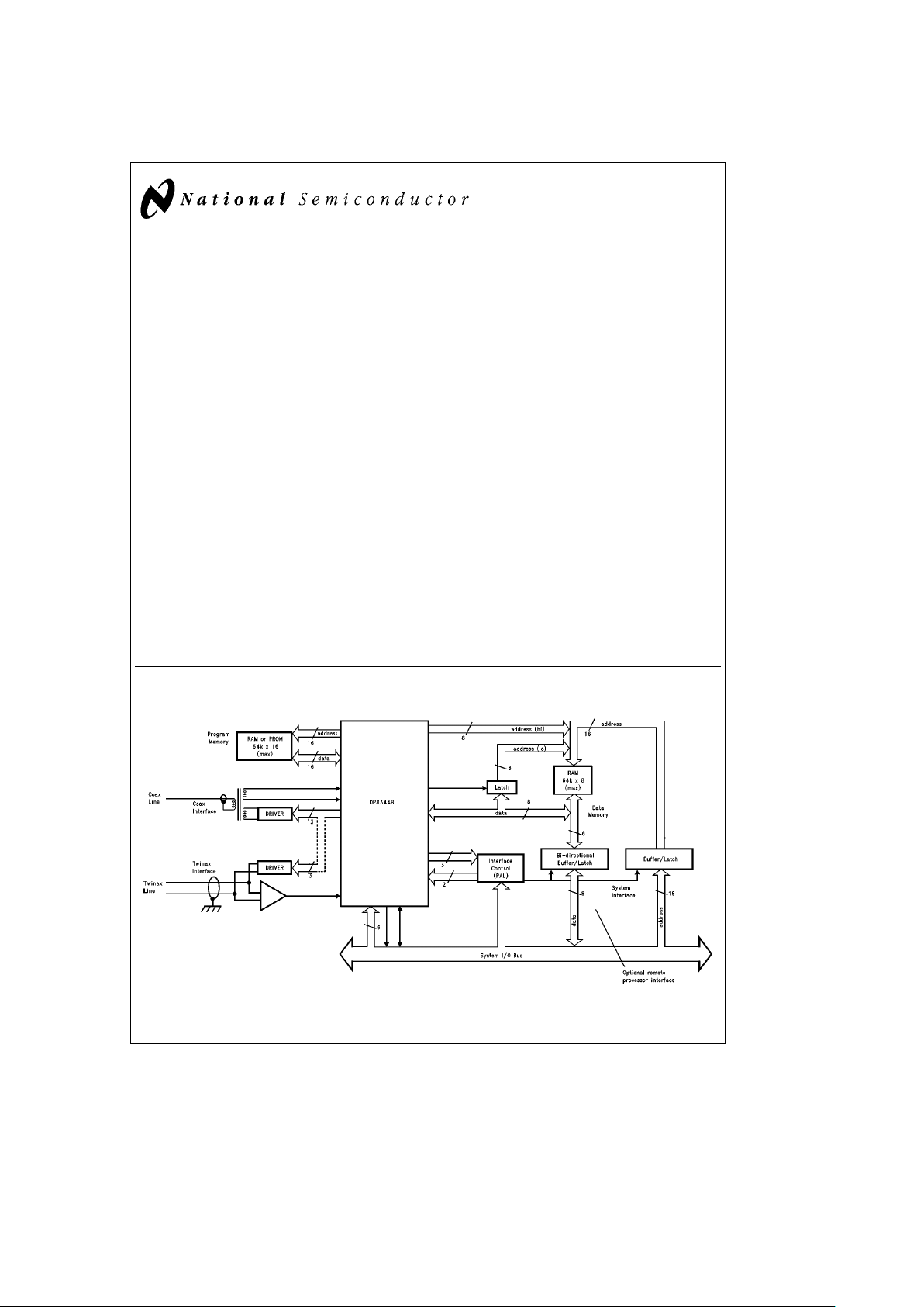
A typical system is shown below. Both coax and twinax line
interfaces are shown, as well as an example of the (optional) remote processor interface.
Features
Transceiver
Y
Software configurable for 3270, 3299, 5250 and general
8-bit protocols
Y
Fully registered status and control
Y
On-chip analog line receiver
Processor
Y
20 MHz clock (50 ns T-states)
Y
Max. instruction cycle: 200 ns
Y
33 instruction types (50 total opcodes)
Y
ALU and barrel shifter
Y
64k x 8 data memory address range
Y
64k x 16 program memory address range
(note: typical system requires
k
2k program memory)
Y
Programmable wait states
Y
Soft-loadable program memory
Y
Interrupt and subroutine capability
Y
Stand alone or host operation
Y
Flexible bus interface with on-chip arbitration logic
General
Y
Low power microCMOS; typ. I
CC
e
25 mA at 20 MHz
Y
84-pin plastic leaded chip carrier (PLCC) package
Block Diagram
Typical BCP System
TL/F/9336– 51
FIGURE 1
BCPÉand TRI-STATEÉare registered trademarks of National Semiconductor Corporation.
IBM
É
is a registered trademark of International Business Machines Corporation.
C
1995 National Semiconductor Corporation RRD-B30M105/Printed in U. S. A.

The DP8344B is an enhanced version of the DP8344A, exhibiting improved switching performance and additional
functionality. The device has been been characterized in a number of applications and found to be a compatible
replacement for the DP8344A. Differences between the DP8344A and DP8344B are noted by shading of the text on the
pages of this data sheet. For more information, refer to Section 6.6.
Note: In this document[XXX]denotes a control or status bit in a register,
À
YYYÓdenotes a register.
Table of Contents
1.0 COMMUNICATIONS PROCESSOR OVERVIEW
1.1 Communications Protocols
1.2 Internal Architecture Overview
1.3 Timing Overview
1.4 Data Flow
1.5 Remote Interface Overview
2.0 CPU DESCRIPTION
2.1 CPU Architectural Description
2.1.1 Register Set
2.1.1.1 Banked Registers
2.1.1.2 Timing Control Registers
2.1.1.3 Interrupt Control Registers
2.1.1.4 Timer Registers
2.1.1.5 Transceiver Registers
2.1.1.6 Condition Code/Remote Handshaking
Register
2.1.1.7 Index Registers
2.1.1.8 Stack Registers
2.1.2 Timer
2.1.2.1 Timer Operation
2.1.3 Instruction Set
2.1.3.1 Harvard Architecture Implications
2.1.3.2 Addressing Modes
2.1.3.3 Instruction Set Overview
2.2 Functional Description
2.2.1 ALU
2.2.2 Timing
2.2.3 Interrupts
2.2.4 Oscillator
3.0 TRANSCEIVER
3.1 Transceiver Architectural Description
3.1.1 Protocols
3.1.1.1 IBM 3270
3.1.1.2 IBM 3299
3.1.1.3 IBM 5250
3.1.1.4 General Purpose 8-Bit
3.2 Transceiver Functional Description
3.2.1 Transmitter
3.2.2 Receiver
3.2.3 Transceiver Interrupts
3.2.4 Protocol Modes
3.2.5 Line Interface
3.2.5.1 3270 Line Interface
3.2.5.2 5250 Line Interface
4.0 REMOTE INTERFACE AND ARBITRATION SYSTEM
(RIAS)
4.1 RIAS Architectural Description
4.1.1 Remote Arbitration Phases
4.1.2 Access Types
4.1.3 Interface Modes
4.1.4 Execution Control
4.2 RIAS Functional Description
4.2.1 Buffered Read
4.2.2 Latched Read
4.2.3 Slow Buffered Write
4.2.4 Fast Buffered Write
4.2.5 Latched Write
4.2.6 Remote Rest Time
2

Table of Contents (Continued)
5.0 DEVICE SPECIFICATIONS
5.1 Pin Description
5.1.1 Timing/Control Signals
5.1.2 Instruction Memory Interface
5.1.3 Data Memory Interface
5.1.4 Transceiver Interface
5.1.5 Remote Interface
5.1.6 External Interrupts
5.2 Absolute Maximum Ratings
5.3 Operating Conditions
5.4 Electrical Characteristics
5.5 Switching Characteristics
5.5.1 Definitions
5.5.2 Timing Tables and Figures
6.0 REFERENCE SECTION
6.1 Instruction Set Reference
6.2 Register Set Reference
6.2.1 Bit Index
6.2.2 Register Description
6.2.3 Bit Definition Tables
6.2.3.1 Processor
6.2.3.2 Transceiver
6.3 Remote Interface Reference
6.4 Development Tools
6.4.1 Assembler System
6.4.2 Development Kit
6.4.3 Multi-Protocol Adapter Design/Evaluation Kit
6.4.4 Inverse Assembler
6.5 3rd Party Suppliers
6.5.1 Crystal
6.5.2 System Development Tools
6.6 DP8344A Compatibility Guide
6.6.1 CPU Timing Changes
6.6.2 Additional Functionality
6.6.2.1 4 T-state Read
6.6.2.2 A/AD Reset State
6.6.2.3 RIC
6.6.2.4 Transceiver
6.7 Reported Bugs
6.7.1 History
6.7.2 LJMP, LCALL Address Decode
6.7.2.1 Suggested Work-around
6.8 Glossary
6.9 Physical Dimensions
3

List of Illustrations
Block Diagram of Typical BCP System АААААААААААААААААААААААААААААААААААААААААААААААААААААААААААААААААААААААААААААА1
Biphase EncodingАААААААААААААААААААААААААААААААААААААААААААААААААААААААААААААААААААААААААААААААААААААААААААААА1-1
IBM 3270 Message FormatАААААААААААААААААААААААААААААААААААААААААААААААААААААААААААААААААААААААААААААААААААААА1-2
Simplified Block DiagramАААААААААААААААААААААААААААААААААААААААААААААААААААААААААААААААААААААААААААААААААААААААА1-3
Memory Configuration АААААААААААААААААААААААААААААААААААААААААААААААААААААААААААААААААААААААААААААААААААААААААА1-4
Effect of Memory Wait States on TimingААААААААААААААААААААААААААААААААААААААААААААААААААААААААААААААААААААААААААА1-5
Register to Register Internal Data Flow АААААААААААААААААААААААААААААААААААААААААААААААААААААААААААААААААААААААААА1-6a
Data Memory WRITE Data Flow АААААААААААААААААААААААААААААААААААААААААААААААААААААААААААААААААААААААААААААААА1-6b
Data Memory READ Data Flow ААААААААААААААААААААААААААААААААААААААААААААААААААААААААААААААААААААААААААААААААА1-6c
WRITE to Transmitter Data Flow АААААААААААААААААААААААААААААААААААААААААААААААААААААААААААААААААААААААААААААААА1-6d
READ from Receiver Data FlowААААААААААААААААААААААААААААААААААААААААААААААААААААААААААААААААААААААААААААААААА1-6e
Load Immediate Data Data FlowААААААААААААААААААААААААААААААААААААААААААААААААААААААААААААААААААААААААААААААААА1-6f
Basic Remote Interface ААААААААААААААААААААААААААААААААААААААААААААААААААААААААААААААААААААААААААААААААААААААААА1-7
Register Map АААААААААААААААААААААААААААААААААААААААААААААААААААААААААААААААААААААААААААААААААААААААААААААААААА2-1
Timer Block Diagram ААААААААААААААААААААААААААААААААААААААААААААААААААААААААААААААААААААААААААААААААААААААААААА2-2
Timer Interrupt DiagramААААААААААААААААААААААААААААААААААААААААААААААААААААААААААААААААААААААААААААААААААААААААА2-3
Index Register MapААААААААААААААААААААААААААААААААААААААААААААААААААААААААААААААААААААААААААААААААААААААААААААА2-4
Coding Examples of Equivalent Conditional Jump Instructions ААААААААААААААААААААААААААААААААААААААААААААААААААААААА2-5
JRMK Instruction Example АААААААААААААААААААААААААААААААААААААААААААААААААААААААААААААААААААААААААААААААААААААА2-6
Condition Code Register ALU Flags АААААААААААААААААААААААААААААААААААААААААААААААААААААААААААААААААААААААААААААА2-7
Carry and Overflow Calculations ААААААААААААААААААААААААААААААААААААААААААААААААААААААААААААААААААААААААААААААААА2-8
Shifts’ Effect on Carry АААААААААААААААААААААААААААААААААААААААААААААААААААААААААААААААААААААААААААААААААААААААААА2-9
Rotates’ Effect on Carry ААААААААААААААААААААААААААААААААААААААААААААААААААААААААААААААААААААААААААААААААААААААА2-10
Multi-Byte Arithmetic Instruction Sequences АААААААААААААААААААААААААААААААААААААААААААААААААААААААААААААААААААААА2-11
CPU-CLK Synchronization with X1 АААААААААААААААААААААААААААААААААААААААААААААААААААААААААААААААААААААААААААААА2-12
Changing from OCLK/2 to OCLKАААААААААААААААААААААААААААААААААААААААААААААААААААААААААААААААААААААААААААААААА2-13
Two T-state Instruction АААААААААААААААААААААААААААААААААААААААААААААААААААААААААААААААААААААААААААААААААААААААА2-14
Three T-state Instruction ААААААААААААААААААААААААААААААААААААААААААААААААААААААААААААААААААААААААААААААААААААААА2-15
Three T-state Data Memory Write Instruction ААААААААААААААААААААААААААААААААААААААААААААААААААААААААААААААААААААА2-16
Three T-state Data Memory Read Instruction ААААААААААААААААААААААААААААААААААААААААААААААААААААААААААААААААААААА2-17
Four T-state Data Memory Read Instruction АААААААААААААААААААААААААААААААААААААААААААААААААААААААААААААААААААААА2-18
Four T-state Program Control Instruction ААААААААААААААААААААААААААААААААААААААААААААААААААААААААААААААААААААААААА2-19
Four T-state Two Word Instruction АААААААААААААААААААААААААААААААААААААААААААААААААААААААААААААААААААААААААААААА2-20
Data Memory Write with One Wait State ААААААААААААААААААААААААААААААААААААААААААААААААААААААААААААААААААААААААА2-21
Data Memory Read with One Wait State ААААААААААААААААААААААААААААААААААААААААААААААААААААААААААААААААААААААААА2-22
Data Memory Read with Two Wait States АААААААААААААААААААААААААААААААААААААААААААААААААААААААААААААААААААААААА2-23
Two T-state Instruction with Two Wait States ААААААААААААААААААААААААААААААААААААААААААААААААААААААААААААААААААААА2-24
Four T-state Instruction with One Wait State АААААААААААААААААААААААААААААААААААААААААААААААААААААААААААААААААААААА2-25
Data Memory Access Wait TimingААААААААААААААААААААААААААААААААААААААААААААААААААААААААААААААААААААААААААААААА2-26
Two T-state Instruction WAIT Timing АААААААААААААААААААААААААААААААААААААААААААААААААААААААААААААААААААААААААААА2-27
Three T-state Program Control Instruction WAIT Timing АААААААААААААААААААААААААААААААААААААААААААААААААААААААААААА2-28
Four T-state Program Control Instruction WAIT Timing ААААААААААААААААААААААААААААААААААААААААААААААААААААААААААААА2-29
LOCK Timing ААААААААААААААААААААААААААААААААААААААААААААААААААААААААААААААААААААААААААААААААААААААААААААААААА2-30
LOCK Timing with One Wait State ААААААААААААААААААААААААААААААААААААААААААААААААААААААААААААААААААААААААААААААА2-31
CPU Start-Up Timing АААААААААААААААААААААААААААААААААААААААААААААААААААААААААААААААААААААААААААААААААААААААААА2-32
Functional State Diagram of CPU Timing ААААААААААААААААААААААААААААААААААААААААААААААААААААААААААААААААААААААААА2-33
Interrupt TimingААААААААААААААААААААААААААААААААААААААААААААААААААААААААААААААААААААААААААААААААААААААААААААААА2-34
DP8344B Operation with Crystal АААААААААААААААААААААААААААААААААААААААААААААААААААААААААААААААААААААААААААААААА2-35
DP8344B Operation with External Clock ААААААААААААААААААААААААААААААААААААААААААААААААААААААААААААААААААААААААА2-36
4

List of Illustrations (Continued)
System Block Diagram, Showing Details of Line Interface ААААААААААААААААААААААААААААААААААААААААААААААААААААААААААА3-1
Biphase EncodingАААААААААААААААААААААААААААААААААААААААААААААААААААААААААААААААААААААААААААААААААААААААААААААА3-2
3270/3299 Protocol Framing Format ААААААААААААААААААААААААААААААААААААААААААААААААААААААААААААААААААААААААААААА3-3
5250 Protocol Framing FormatААААААААААААААААААААААААААААААААААААААААААААААААААААААААААААААААААААААААААААААААААА3-4
General Purpose 8-Bit Protocol Framing FormatАААААААААААААААААААААААААААААААААААААААААААААААААААААААААААААААААААА3-5
Block Diagram of Transceiver, Showing CPU Interface АААААААААААААААААААААААААААААААААААААААААААААААААААААААААААААА3-6
Transmitter Output ААААААААААААААААААААААААААААААААААААААААААААААААААААААААААААААААААААААААААААААААААААААААААААА3-7
Timing of Receiver Flags Relative to Incoming Data АААААААААААААААААААААААААААААААААААААААААААААААААААААААААААААААА3-8
3270, 3299 Frame Assembly/Disassembly DescriptionАААААААААААААААААААААААААААААААААААААААААААААААААААААААААААААА3-9
5250 Frame Assembly/Disassembly Description АААААААААААААААААААААААААААААААААААААААААААААААААААААААААААААААААА3-10
General Purpose 8-Bit Frame Assembly/Disassembly Description ААААААААААААААААААААААААААААААААААААААААААААААААААА3-11
BCP Receiver DesignАААААААААААААААААААААААААААААААААААААААААААААААААААААААААААААААААААААААААААААААААААААААААА3-12
BCP Driver Design АААААААААААААААААААААААААААААААААААААААААААААААААААААААААААААААААААААААААААААААААААААААААААА3-13
BCP Coax/Twisted Pair Front End АААААААААААААААААААААААААААААААААААААААААААААААААААААААААААААААААААААААААААААА3-14
5250 Line Interface SchematicАААААААААААААААААААААААААААААААААААААААААААААААААААААААААААААААААААААААААААААААААА3-15
Remote Interface Processor ААААААААААААААААААААААААААААААААААААААААААААААААААААААААААААААААААААААААААААААААААААА4-1
Remote Interface Control Register ААААААААААААААААААААААААААААААААААААААААААААААААААААААААААААААААААААААААААААААА4-2
Generic Remote Access АААААААААААААААААААААААААААААААААААААААААААААААААААААААААААААААААААААААААААААААААААААААА4-3
Generic RIC Access АААААААААААААААААААААААААААААААААААААААААААААААААААААААААААААААААААААААААААААААААААААААААААА4-4
Memory Select Bits in
À
RICУААААААААААААААААААААААААААААААААААААААААААААААААААААААААААААААААААААААААААААААААААААА4-5
Generic DMEM Access ААААААААААААААААААААААААААААААААААААААААААААААААААААААААААААААААААААААААААААААААААААААААА4-6
Generic PC AccessААААААААААААААААААААААААААААААААААААААААААААААААААААААААААААААААААААААААААААААААААААААААААААА4-7
Generic IMEM Access АААААААААААААААААААААААААААААААААААААААААААААААААААААААААААААААААААААААААААААААААААААААААА4-8
Read from Remote Processor ААААААААААААААААААААААААААААААААААААААААААААААААААААААААААААААААААААААААААААААААААА4-9
Buffered Write from Remote Processor АААААААААААААААААААААААААААААААААААААААААААААААААААААААААААААААААААААААААА4-10
Latched Write from Remote ProcessorААААААААААААААААААААААААААААААААААААААААААААААААААААААААААААААААААААААААААА4-11
Minimum BCP/Remote Processor Interface АААААААААААААААААААААААААААААААААААААААААААААААААААААААААААААААААААААА4-12
Interface Mode Bits ААААААААААААААААААААААААААААААААААААААААААААААААААААААААААААААААААААААААААААААААААААААААААА4-13
Flow Chart of Buffered Read Mode АААААААААААААААААААААААААААААААААААААААААААААААААААААААААААААААААААААААААААААА4-14
Buffered Read of Data Memory by Remote Processor ААААААААААААААААААААААААААААААААААААААААААААААААААААААААААААА4-15
Flow Chart of Latched Read Mode АААААААААААААААААААААААААААААААААААААААААААААААААААААААААААААААААААААААААААААА4-16
Latched Read of Data Memory by Remote Processor АААААААААААААААААААААААААААААААААААААААААААААААААААААААААААААА4-17
Flow Chart of Slow Buffered Write Mode ААААААААААААААААААААААААААААААААААААААААААААААААААААААААААААААААААААААААА4-18
Slow Buffered Write to Data Memory by Remote ProcessorААААААААААААААААААААААААААААААААААААААААААААААААААААААААА4-19
Flow Chart of Fast Buffered Write ModeАААААААААААААААААААААААААААААААААААААААААААААААААААААААААААААААААААААААААА4-20
Fast Buffered Write to Data Memory by Remote Processor ААААААААААААААААААААААААААААААААААААААААААААААААААААААААА4-21
Flow Chart of Latched Write Mode АААААААААААААААААААААААААААААААААААААААААААААААААААААААААААААААААААААААААААААА4-22
Latched Write to Data Memory by Remote Processor АААААААААААААААААААААААААААААААААААААААААААААААААААААААААААААА4-23
Mistaking Two Remote Accesses as Only OneАААААААААААААААААААААААААААААААААААААААААААААААААААААААААААААААААААА4-24
Remote Rest Time for All Modes Except Latched Write АААААААААААААААААААААААААААААААААААААААААААААААААААААААААААА4-25
Rest Time for Latched Write Mode АААААААААААААААААААААААААААААААААААААААААААААААААААААААААААААААААААААААААААААА4-26
DP8344B Top ViewААААААААААААААААААААААААААААААААААААААААААААААААААААААААААААААААААААААААААААААААААААААААААААА5-1
Switching Characteristic Measurement Waveforms ААААААААААААААААААААААААААААААААААААААААААААААААААААААААААААААААА5-2
Data Memory Read Timing АААААААААААААААААААААААААААААААААААААААААААААААААААААААААААААААААААААААААААААААААААААА5-3
Data Memory Write Timing АААААААААААААААААААААААААААААААААААААААААААААААААААААААААААААААААААААААААААААААААААААА5-4
Instruction Memory Timing АААААААААААААААААААААААААААААААААААААААААААААААААААААААААААААААААААААААААААААААААААААА5-5
Clock Timing АААААААААААААААААААААААААААААААААААААААААААААААААААААААААААААААААААААААААААААААААААААААААААААААААА5-6
5

List of Illustrations (Continued)
Transceiver Timing ААААААААААААААААААААААААААААААААААААААААААААААААААААААААААААААААААААААААААААААААААААААААААААА5-7
Analog and DATA-IN Timing ААААААААААААААААААААААААААААААААААААААААААААААААААААААААААААААААААААААААААААААААААААА5-8
Interrupt Timing АААААААААААААААААААААААААААААААААААААААААААААААААААААААААААААААААААААААААААААААААААААААААААААААА5-9
Control Pin Timing АААААААААААААААААААААААААААААААААААААААААААААААААААААААААААААААААААААААААААААААААААААААААААА5-10
Buffered Read of PC, RIC АААААААААААААААААААААААААААААААААААААААААААААААААААААААААААААААААААААААААААААААААААААА5-11
Buffered Read of DMEM ААААААААААААААААААААААААААААААААААААААААААААААААААААААААААААААААААААААААААААААААААААААА5-12
Buffered Read of IMEM АААААААААААААААААААААААААААААААААААААААААААААААААААААААААААААААААААААААААААААААААААААААА5-13
Latched Read of PC, RIC АААААААААААААААААААААААААААААААААААААААААААААААААААААААААААААААААААААААААААААААААААААА5-14
Latched Read of DMEM ААААААААААААААААААААААААААААААААААААААААААААААААААААААААААААААААААААААААААААААААААААААА5-15
Latched Read of IMEM АААААААААААААААААААААААААААААААААААААААААААААААААААААААААААААААААААААААААААААААААААААААА5-16
Slow Buffered Write of PC, RIC ААААААААААААААААААААААААААААААААААААААААААААААААААААААААААААААААААААААААААААААААА5-17
Slow Buffered Write of DMEM АААААААААААААААААААААААААААААААААААААААААААААААААААААААААААААААААААААААААААААААААА5-18
Slow Buffered Write of IMEM ААААААААААААААААААААААААААААААААААААААААААААААААААААААААААААААААААААААААААААААААААА5-19
Fast Buffered Write of PC, RICАААААААААААААААААААААААААААААААААААААААААААААААААААААААААААААААААААААААААААААААААА5-20
Fast Buffered Write of DMEMААААААААААААААААААААААААААААААААААААААААААААААААААААААААААААААААААААААААААААААААААА5-21
Fast Buffered Write of IMEM ААААААААААААААААААААААААААААААААААААААААААААААААААААААААААААААААААААААААААААААААААА5-22
Latched Write of PC, RICААААААААААААААААААААААААААААААААААААААААААААААААААААААААААААААААААААААААААААААААААААААА5-23
Latched Write of DMEM ААААААААААААААААААААААААААААААААААААААААААААААААААААААААААААААААААААААААААААААААААААААА5-24
Latched Write of IMEM АААААААААААААААААААААААААААААААААААААААААААААААААААААААААААААААААААААААААААААААААААААААА5-25
Remote Rest Times ААААААААААААААААААААААААААААААААААААААААААААААААААААААААААААААААААААААААААААААААААААААААААА5-26
Remote Interface WAIT Timing ААААААААААААААААААААААААААААААААААААААААААААААААААААААААААААААААААААААААААААААААА5-27
WAIT Timing after Remote Access АААААААААААААААААААААААААААААААААААААААААААААААААААААААААААААААААААААААААААААА5-28
Instruction Memory Bus Timing for 2 T-state Instructions АААААААААААААААААААААААААААААААААААААААААААААААААААААААААААА6-1
Instruction Memory Bus Timing for 3 T-state Instructions АААААААААААААААААААААААААААААААААААААААААААААААААААААААААААА6-2
Instruction Memory Bus Timing for (2
a
2) T-state Instructions АААААААААААААААААААААААААААААААААААААААААААААААААААААААА6-3
Instruction Memory Bus Timing for 4 T-state Instructions АААААААААААААААААААААААААААААААААААААААААААААААААААААААААААА6-4
Instruction/Data Memory Bus Timing for Data Memory Read[4TR
]
e
0ААААААААААААААААААААААААААААААААААААААААААААААА6-5
Instruction/Data Memory Bus Timing for Data Memory Read[4TR
]
e
1ААААААААААААААААААААААААААААААААААААААААААААААА6-6
Instruction/Data Memory Bus Timing for Data Memory WriteААААААААААААААААААААААААААААААААААААААААААААААААААААААААА6-7
List of Tables
Register Addressing Mode Notations ААААААААААААААААААААААААААААААААААААААААААААААААААААААААААААААААААААААААААААА2-1
Immediate Addressing Mode Notations ААААААААААААААААААААААААААААААААААААААААААААААААААААААААААААААААААААААААААА2-2
Index Register Addressing Mode Notations АААААААААААААААААААААААААААААААААААААААААААААААААААААААААААААААААААААААА2-3
Relative Index Register Mode NotationsААААААААААААААААААААААААААААААААААААААААААААААААААААААААААААААААААААААААААА2-4
Data Movement NotationsААААААААААААААААААААААААААААААААААААААААААААААААААААААААААААААААААААААААААААААААААААААА2-5
Integer Arithmetic Instruction АААААААААААААААААААААААААААААААААААААААААААААААААААААААААААААААААААААААААААААААААААА2-6
Logic Instructions АААААААААААААААААААААААААААААААААААААААААААААААААААААААААААААААААААААААААААААААААААААААААААААА2-7
Shift and Rotate InstructionsААААААААААААААААААААААААААААААААААААААААААААААААААААААААААААААААААААААААААААААААААААА2-8
Comparison Instructions АААААААААААААААААААААААААААААААААААААААААААААААААААААААААААААААААААААААААААААААААААААААА2-9
Unconditional Jump Instructions АААААААААААААААААААААААААААААААААААААААААААААААААААААААААААААААААААААААААААААААА2-10
Conditional Relative Jump InstructionsААААААААААААААААААААААААААААААААААААААААААААААААААААААААААААААААААААААААААА2-11
‘‘f’’ FlagsААААААААААААААААААААААААААААААААААААААААААААААААААААААААААААААААААААААААААААААААААААААААААААААААААААА2-12
‘‘cc’’ Conditions Tested АААААААААААААААААААААААААААААААААААААААААААААААААААААААААААААААААААААААААААААААААААААААА2-13
Conditional Absolute Jump Instructions АААААААААААААААААААААААААААААААААААААААААААААААААААААААААААААААААААААААААА2-14
JRMK Instruction ААААААААААААААААААААААААААААААААААААААААААААААААААААААААААААААААААААААААААААААААААААААААААААА2-15
Unconditional Call InstructionsАААААААААААААААААААААААААААААААААААААААААААААААААААААААААААААААААААААААААААААААААА2-16
Conditional Call Instructions АААААААААААААААААААААААААААААААААААААААААААААААААААААААААААААААААААААААААААААААААААА2-17
Unconditional Return Instruction АААААААААААААААААААААААААААААААААААААААААААААААААААААААААААААААААААААААААААААААА2-18
Conditional Return Instruction АААААААААААААААААААААААААААААААААААААААААААААААААААААААААААААААААААААААААААААААААА2-19
TRAP InstructionАААААААААААААААААААААААААААААААААААААААААААААААААААААААААААААААААААААААААААААААААААААААААААААА2-20
EXX Instruction ААААААААААААААААААААААААААААААААААААААААААААААААААААААААААААААААААААААААААААААААААААААААААААААА2-21
6

List of Tables (Continued)
Unsigned Comparison Results АААААААААААААААААААААААААААААААААААААААААААААААААААААААААААААААААААААААААААААААААА2-22
Signed Comparison Results АААААААААААААААААААААААААААААААААААААААААААААААААААААААААААААААААААААААААААААААААААА2-23
Data Memory Wait States АААААААААААААААААААААААААААААААААААААААААААААААААААААААААААААААААААААААААААААААААААААА2-24
Instruction Memory Wait States ААААААААААААААААААААААААААААААААААААААААААААААААААААААААААААААААААААААААААААААААА2-25
BIRQ Control Summary АААААААААААААААААААААААААААААААААААААААААААААААААААААААААААААААААААААААААААААААААААААААА2-26
À
ICRУInterrupt Mask Bits and Interrupt PriorityАААААААААААААААААААААААААААААААААААААААААААААААААААААААААААААААААААА2-27
Interrupt Vector Generation АААААААААААААААААААААААААААААААААААААААААААААААААААААААААААААААААААААААААААААААААААА2-28
Recommended Crystal ParametersАААААААААААААААААААААААААААААААААААААААААААААААААААААААААААААААААААААААААААААА2-29
Protocol Mode Definitions ААААААААААААААААААААААААААААААААААААААААААААААААААААААААААААААААААААААААААААААААААААААА3-1
Transceiver Interrupts АААААААААААААААААААААААААААААААААААААААААААААААААААААААААААААААААААААААААААААААААААААААААА3-2
Receiver Interrupts ААААААААААААААААААААААААААААААААААААААААААААААААААААААААААААААААААААААААААААААААААААААААААААА3-3
Decode of 3270 Coax Commands АААААААААААААААААААААААААААААААААААААААААААААААААААААААААААААААААААААААААААААААА3-4
RIAS Inputs and Outputs АААААААААААААААААААААААААААААААААААААААААААААААААААААААААААААААААААААААААААААААААААААААА4-1
Note: To match Timing table number with appropriate Timing illustration, Tables 5-1 and 5-2 are purposely omitted.
Data Memory Read Timing АААААААААААААААААААААААААААААААААААААААААААААААААААААААААААААААААААААААААААААААААААААА5-3
Data Memory Write Timing АААААААААААААААААААААААААААААААААААААААААААААААААААААААААААААААААААААААААААААААААААААА5-4
Instruction Memory Timing АААААААААААААААААААААААААААААААААААААААААААААААААААААААААААААААААААААААААААААААААААААА5-5
Clock Timing АААААААААААААААААААААААААААААААААААААААААААААААААААААААААААААААААААААААААААААААААААААААААААААААААА5-6
Transceiver Timing ААААААААААААААААААААААААААААААААААААААААААААААААААААААААААААААААААААААААААААААААААААААААААААА5-7
Analog and DATA-IN Timing ААААААААААААААААААААААААААААААААААААААААААААААААААААААААААААААААААААААААААААААААААААА5-8
Interrupt Timing АААААААААААААААААААААААААААААААААААААААААААААААААААААААААААААААААААААААААААААААААААААААААААААААА5-9
Control Pin Timing АААААААААААААААААААААААААААААААААААААААААААААААААААААААААААААААААААААААААААААААААААААААААААА5-10
Buffered Read of PC, RIC АААААААААААААААААААААААААААААААААААААААААААААААААААААААААААААААААААААААААААААААААААААА5-11
Buffered Read of DMEM ААААААААААААААААААААААААААААААААААААААААААААААААААААААААААААААААААААААААААААААААААААААА5-12
Buffered Read of IMEM АААААААААААААААААААААААААААААААААААААААААААААААААААААААААААААААААААААААААААААААААААААААА5-13
Latched Read of PC, RIC АААААААААААААААААААААААААААААААААААААААААААААААААААААААААААААААААААААААААААААААААААААА5-14
Latched Read of DMEM ААААААААААААААААААААААААААААААААААААААААААААААААААААААААААААААААААААААААААААААААААААААА5-15
Latched Read of IMEM АААААААААААААААААААААААААААААААААААААААААААААААААААААААААААААААААААААААААААААААААААААААА5-16
Slow Buffered Write of PC, RIC ААААААААААААААААААААААААААААААААААААААААААААААААААААААААААААААААААААААААААААААААА5-17
Slow Buffered Write of DMEM АААААААААААААААААААААААААААААААААААААААААААААААААААААААААААААААААААААААААААААААААА5-18
Slow Buffered Write of IMEM ААААААААААААААААААААААААААААААААААААААААААААААААААААААААААААААААААААААААААААААААААА5-19
Fast Buffered Write of PC, RICАААААААААААААААААААААААААААААААААААААААААААААААААААААААААААААААААААААААААААААААААА5-20
Fast Buffered Write of DMEMААААААААААААААААААААААААААААААААААААААААААААААААААААААААААААААААААААААААААААААААААА5-21
Fast Buffered Write of IMEM ААААААААААААААААААААААААААААААААААААААААААААААААААААААААААААААААААААААААААААААААААА5-22
Latched Write of PC, RICААААААААААААААААААААААААААААААААААААААААААААААААААААААААААААААААААААААААААААААААААААААА5-23
Latched Write of DMEM ААААААААААААААААААААААААААААААААААААААААААААААААААААААААААААААААААААААААААААААААААААААА5-24
Latched Write of IMEM АААААААААААААААААААААААААААААААААААААААААААААААААААААААААААААААААААААААААААААААААААААААА5-25
Remote Rest Times ААААААААААААААААААААААААААААААААААААААААААААААААААААААААААААААААААААААААААААААААААААААААААА5-26
Remote Interface WAIT Timing ААААААААААААААААААААААААААААААААААААААААААААААААААААААААААААААААААААААААААААААААА5-27
WAIT Timing after Remote Access АААААААААААААААААААААААААААААААААААААААААААААААААААААААААААААААААААААААААААААА5-28
Notational Conventions for Instruction SetААААААААААААААААААААААААААААААААААААААААААААААААААААААААААААААААААААААААА6-1
Instructions vs T-states, Affected Flags and Bus Timing ААААААААААААААААААААААААААААААААААААААААААААААААААААААААААААА6-2
Instruction Opcodes АААААААААААААААААААААААААААААААААААААААААААААААААААААААААААААААААААААААААААААААААААААААААААА6-3
DP8344B Application Notes ААААААААААААААААААААААААААААААААААААААААААААААААААААААААААААААААААААААААААААААААААААА6-4
7
1.0 Communications Processor Introduction
The increased demand for computer connectivity has driven
National Semiconductor to develop the next generation of
special purpose microprocessors. The DP8344B is the first
example of a ‘‘Communications Processor’’ for the IBM environment. It integrates a very fast, full function microprocessor with highly specialized transceiver circuitry. The combination of speed, power, and features allows the designer
to easily implement a state-of-the-art communications interface. Typical applications for a communications processor
are terminal emulation boards for PCs, stand-alone terminals, printer interfaces, and cluster controllers.
The transceiver is designed to simplify the handling of specific communication protocols. This feature makes it possible to quickly develop interfaces and software with little concern for the ‘‘housekeeping’’ details of the protocol being
used.
1.1 COMMUNICATIONS PROTOCOLS
A communication protocol is a set of rules which defines the
physical, electrical, and software specifications required to
successfully transfer data between two systems.
The physical specification includes the network architecture, as well as the type of connecting medium, the connectors used, and the maximum distance between connections.
Networks may be configured in ‘‘loops,’’ ‘‘stars,’’ or ‘‘daisy
chains,’’ and they often use standard coaxial or twisted-pair
cable.
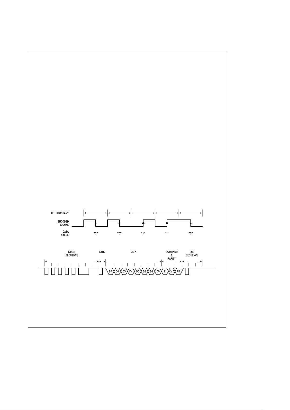
The electrical specification includes the polarity and amplitude of the signal, the frequency (bit rate), and encoding
technique. One common method of encoding is called ‘‘biphase’’ or ‘‘Manchester II.’’ This technique combines the
clock and data information into one transmission by encoding data as a ‘‘mid-bit’’ transition.
Figure 1-1
shows how the
data transition is related to the bit boundary in a typical
transmission. The polarity of the ‘‘mid-bit’’ transition en-
codes the data value, other transitions lie on bit boundaries.
Bit boundaries are not always indicated by transitions, so
techniques employing start sequences and sync bits are
used with bi-phase transmissions to ensure proper frame
alignment and synchronization.
The software specification covers the use of start sequences and sync bits, as well as defining the message
format. Parity bits may be used to ensure data integrity. The
message format is the ‘‘language’’ that is used to exchange
information across the connecting medium. It defines command and control words, response times, and expected responses.
The DP8344B Bi-phase Communications Processor supports both the IBM 3270 and 5250 communication protocols, as well as IBM 3299 and a general purpose 8-bit protocol. The specialized transceiver is combined with a microprocessor whose instruction set is optimized for use in a
communications environment. This makes the DP8344 a
powerful single-chip solution to a wide range of communication applications.
An example of an IBM 3270 message is shown in
Figure
1-2
. The transmission begins with a very specific start sequence and sync pulse for synchronization. This is followed
by the data, command, and parity bits. Finally, the end sequence defines the end of the transmission.
The IBM 3270 and 5250 are two widely used protocols. The
3270 protocol was developed for the 370 class mainframe,
and it employs coaxial cable in a ‘‘star’’ configuration. The
5250 protocol was developed for the System/3x machines,
and it uses a ‘‘daisy-chain’’ of twin-ax cable. A good overview of both of these environments may be found in the
‘‘Multi-Protocol Adapter System User Guide’’ from National
Semiconductor, and in the Transceiver section of this document.
TL/F/9336– B7
FIGURE 1-1. Biphase Encoding
TL/F/9336– B8
FIGURE 1-2. IBM 3270 Message Format
8
1.0 Communications Processor Introduction (Continued)
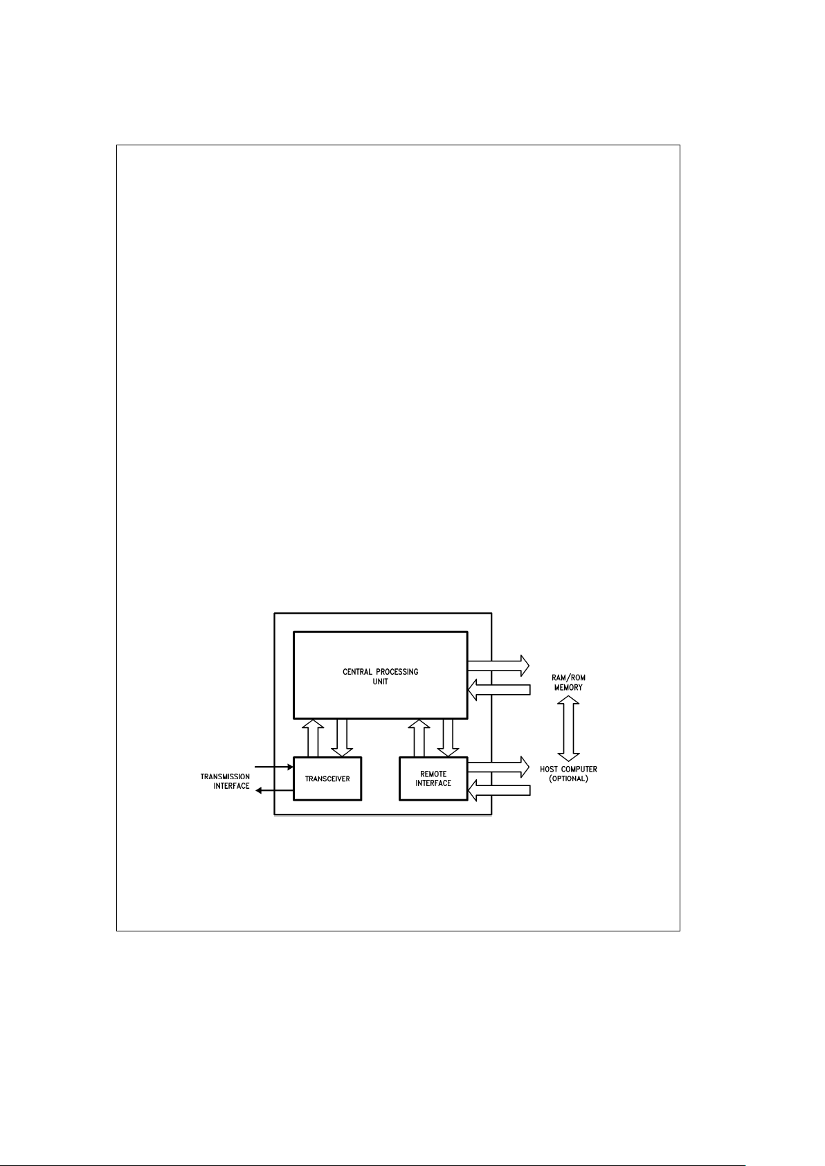
1.2 INTERNAL ARCHITECTURE INTRODUCTION
The DP8344B Biphase Communications Processor (BCP) is
divided into three major functional blocks: the Transceiver,
the Central Processing Unit (CPU), and the Remote Interface and Arbitration System, RIAS.
Figure 1-3
shows how
these blocks are related to each other and to other system
components.
The transceiver consists of an asynchronous transmitter
and receiver which can communicate across a serial data
path. The transmitter takes parallel data from the CPU and
appends to it the appropriate framing information. The resulting message is shifted out and is available as a serial
data stream on two output pins. The receiver shifts in serial
messages, strips off the framing information, and makes the
data available in parallel form to the CPU. The framing information supplied by the BCP provides the proper message
format for several popular communication protocols. These
include IBM 3270, 3299, and 5250, as well as a general
purpose 8-bit mode.
The transceiver clock may be derived from the internal oscillator, either directly or through internal divide-down circuitry. There is also an input for an external transceiver clock,
thus allowing complete flexibility in the choice of data rates.
The receiver input can come from three possible sources.
There is a built-in differential amplifier which is suitable for
most line interfaces, a single-ended digital input for use with
an external comparator, and an internal loopback path for
self testing. Refer to the Transceiver section for a detailed
description of all transmitter and receiver functions, and to
the application note on coax interfaces for the proper use of
the differential amplifier.
The CPU is a general purpose, 8-bit microprocessor capable of 20 MHz operation. It has a reduced instruction set
which is optimized for transceiver and data handling performance. It also has a full function arithmetic/logic unit
(ALU) which performs addition, subtraction, Boolean operations, rotations and shifts. Separate instruction and data
memory systems are supported, each with 16-bit address
buses, for a total of 64k address space in each.
There are 44 internal registers accessible to the CPU.
These include special configuration and control registers for
the transceiver and processor, four 16-bit indices to data
memory, and 20 8-bit general purpose registers. There is
also a 16-bit timer and a 16-byte deep LIFO data stack
which are accessible in the register address space. For
more detailed information, see the specific sections on the
Register set, the Timer, and the ALU.
The BCP can operate independently or with another processor as the host system. If such a system is required, communication with the BCP is possible by sharing data memory. The Remote Interface controls bus arbitration and access to data memory, as well as program up-loading and
execution. For example, it is possible for a host system to
load the BCP’s instruction memory and begin program execution, then pass data back and forth through data memory
accesses. The section on the Remote Interface and Arbitration System provides all of the necessary timing and control
information to implement an interface between a BCP and a
remote system.
As shown in
Figure 1-4,
the BCP uses two entirely separate
memory systems, one for program storage and the other for
data storage. This type of memory arrangement is referred
to as Harvard architecture. Each system has 16 address
lines, for a maximum of 64k words in each, and its own set
of data lines. The instruction (program) memory is two bytes
(16 bits) wide, and the data memory is one byte (8 bits)
wide.
In order to reduce the number of pins required for these
signals, the address and data lines for data memory are
multiplexed together. This requires an external latch and the
Address Latch Enable signal (ALE) for de-multiplexing.
TL/F/9336– B9
FIGURE 1-3. Simplified Block Diagram
9
1.0 Communications Processor Introduction (Continued)
Simultaneous access to both data and program memory,
and instruction pipelining greatly enhance the speed performance of the BCP, making it well suited for real-time processing. The pipeline allows the next instruction to be retrieved from program memory while the current instruction is
being executed.
1.3 TIMING INTRODUCTION
The timing of all CPU operations, instruction execution and
memory access is related to the CPU clock. This clock is
usually generated by a crystal and the internal oscillator,
with optional divide by two circuitry. The period of the resulting CPU clock is referred to as a T-state; for example, a
20 MHz CPU clock yields a 50 ns T-state. Most CPU functions, such as arithmetic and logical operations, shifts and
rotates, and register moves, require only two T-states.
Branching instructions and data memory accesses require
three to four T-states.
Each memory system has a separate, programmable number of wait states to allow the use of slower memory devices. Instruction memory wait states are inserted into all instructions, as shown in
Figure 1-5,
thus they affect the
overall speed of program execution. Instruction memory
wait states can also apply when the Remote Interface is
loading a program into instruction memory. Data memory
wait states are only inserted into data memory access instructions, hence there is less degradation in overall program execution. Refer to the Timing section for detailed examples of all BCP instruction and data memory timing.
TL/F/9336– C1
FIGURE 1-4. Memory Configuration
TL/F/9336– C2
FIGURE 1-5. Effect of Memory Wait States on Timing
10
1.0 Communications Processor Introduction (Continued)
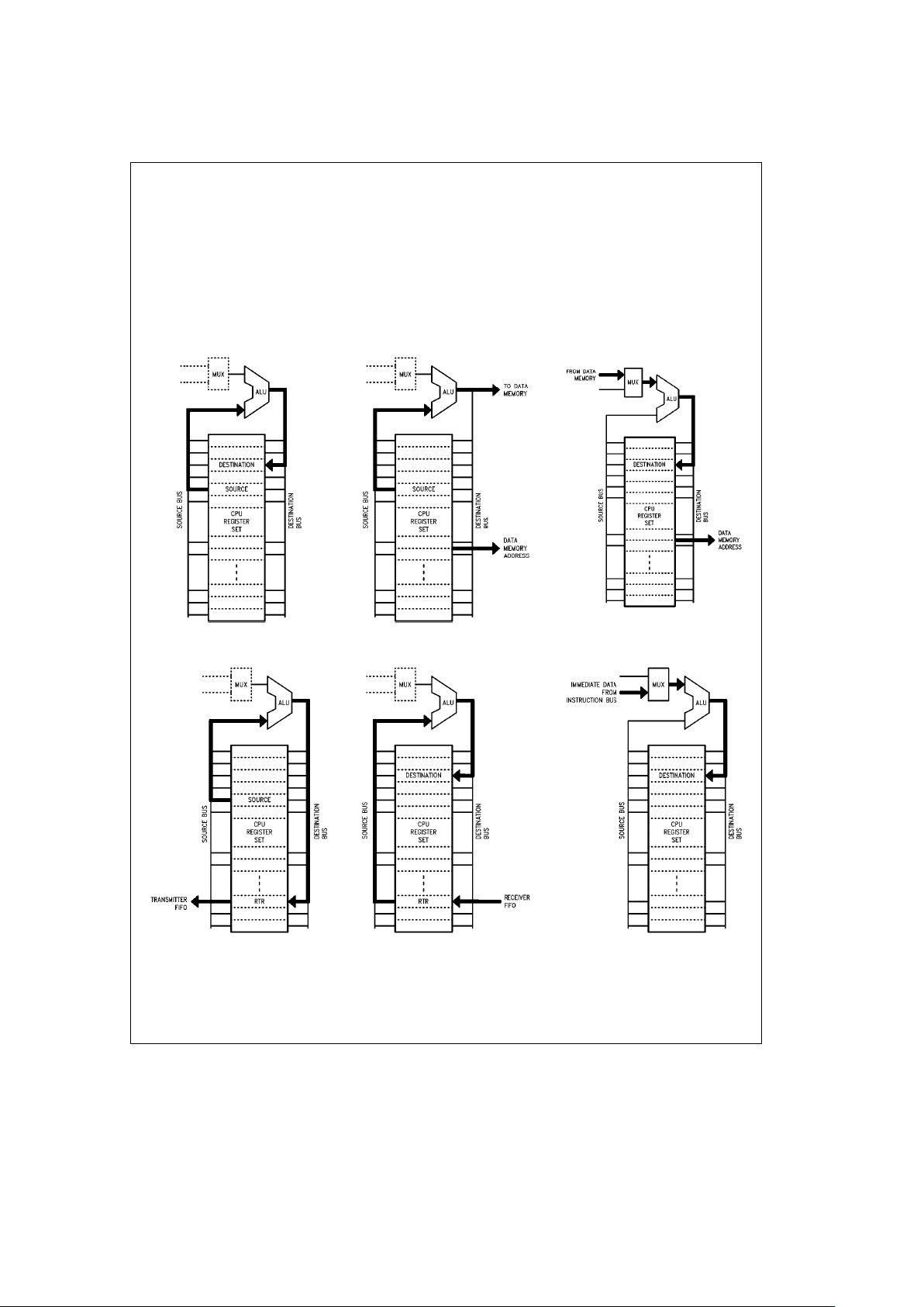
1.4 DATA FLOW
The CPU registers are all dual port, that is, they have separate input and output paths. This arrangement allows a single register to function as both a source and a destination
within the same instruction.
Figures 1-6a
through
1-6f
show the internal data flow path
for the BCP. The CPU registers are a central element to this
path. When a register functions as an output, its contents
are placed on the Source bus. When a register is an input,
data from the Destination bus is written into that register.
The other key element in the data path is the ALU. This unit
does all of the arithmetic and data manipulation operations,
but it also has bus multiplexing capabilities. Both the Data
Memory bus and a portion of the Instruction Memory bus
are routed to this unit and serve as alternative sources of
data. Since the data flow is always through this unit, most
data moves may include arithmetic manipulations with no
penalty in execution time.
Figure 1-6a
shows the data path for all arithmetic instructions and register to register moves. The source register
contents are placed on the Source bus, routed through the
TL/F/9336– C3 TL/F/9336– C4
TL/F/9336– C5
FIGURE 1-6a. Register to Register FIGURE 1-6b. Data Memory WRITE FIGURE 1-6c. Data Memory READ
TL/F/9336– C6 TL/F/9336– C7 TL/F/9336– C8
FIGURE 1-6d. WRITE to Transmitter FIGURE 1-6e. READ from Receiver FIGURE 1-6f. Load Immediate Data
11
1.0 Communications Processor Introduction (Continued)
ALU/MUX, and then placed on the destination bus. This
data is then stored into the appropriate destination register.
Figures 1-6b
and
1-6c
show the data path for data memory
accesses. For a WRITE operation, the source register contents follow the same path through the ALU/MUX, but the
Destination bus is routed to output pins and on to data
memory. For a READ operation, incoming data is routed
onto the Destination bus by the ALU/MUX, and then stored
in a register. The address for all data memory accesses is
provided by one of four 16-bit index registers which can
operate in a variety of automatic increment and decrement
modes.
Transfer of the data byte between the CPU and the Transceiver is accomplished through a register location. This register,
À
RTRÓ, appears as a normal CPU register, but writing
to it automatically transfers data to the transmitter FIFO,
and reading from it retrieves data from the receiver FIFO.
These paths are illustrated in
Figures 1-6d
and
1-6e.
It is also possible to load immediate data into a CPU register. This data is supplied by the program and is usually a
constant such as a pointer or character. As shown in
Figure
1-6f,
a portion of the Instruction bus is routed through the
ALU/MUX for this purpose.
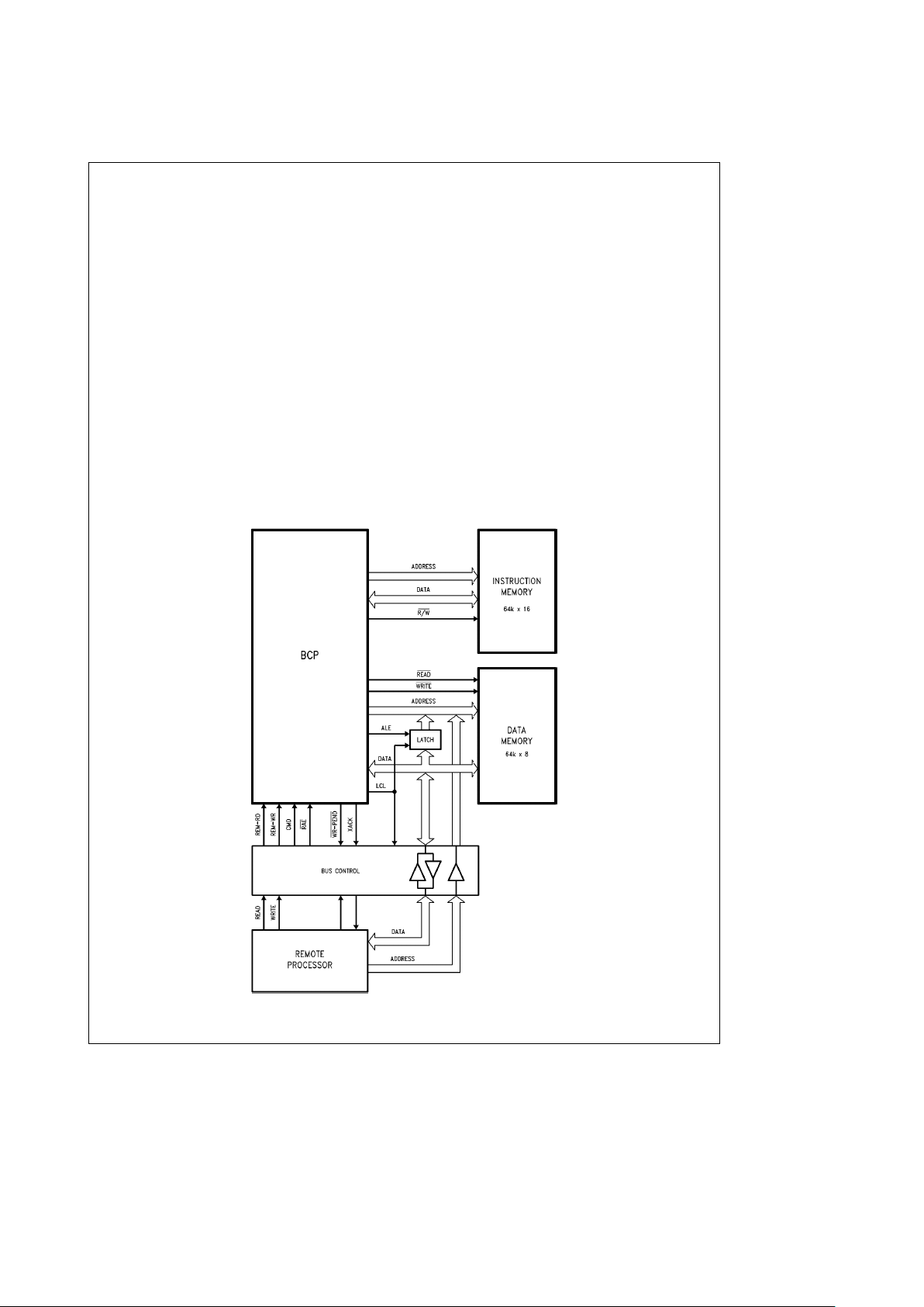
1.5 REMOTE INTERFACE AND ARBITRATION SYSTEM
INTRODUCTION
The BCP is designed to serve as a complete, stand alone
communications interface. Alternately, it can be interfaced
with another processor by means of the Remote Interface
and Arbitration System. Communication between the BCP
and the remote processor is possible by sharing data memory. Harvard architecture allows the remote system to access any BCP data memory location while the BCP continues to fetch and execute instructions, thereby minimizing
performance degradation.
Figure 1-7
shows a simplified remote processor interface.
This includes tri-state buffers on the address and data buses of the BCP’s Data Memory, and all of the control and
handshaking signals required to communicate between the
BCP and the host system.
There is an 8-bit control register, Remote Interface Control
À
RICÓ, accessible only to the remote system, which is used
to control a variety of features, including the types of memory accesses, interface speeds, single step program execution, CPU start/stop, instruction memory loads, and so forth.
Detailed information on all interface options is provided in
the section on Remote Interface and Arbitration System,
and in the related Reference section.
TL/F/9336– C9
FIGURE 1-7. Basic Remote Interface
12
2.0 CPU Description
The CPU is a general purpose, 8-bit microprocessor capable of 20 MHz operation. It contains a large register set for
standard CPU operations and control of the transceiver.
The reduced instruction set is optimized for the communications environment. The following sections are an architectural and functional description of the DP8344B CPU.
2.1 CPU ARCHITECTURAL DESCRIPTION
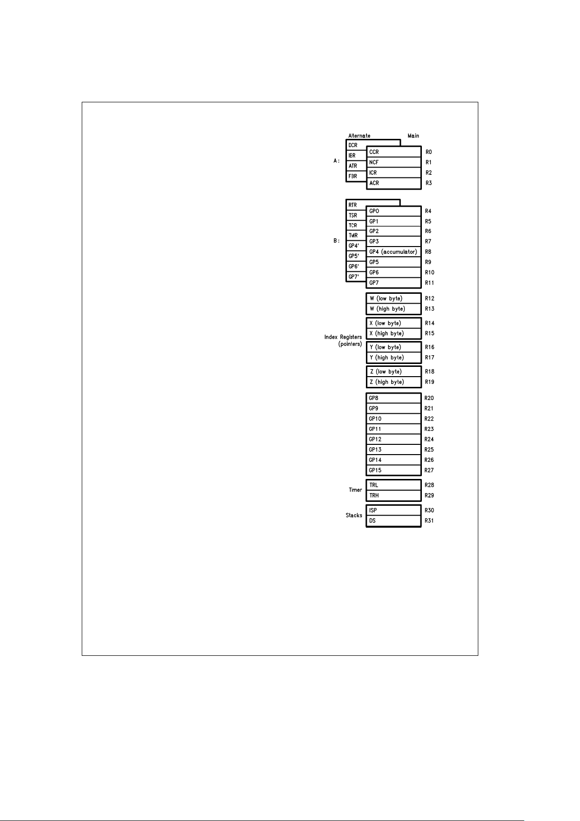
2.1.1 Register Set
This section describes the BCP’s internal CPU registers. It is
a general overview of the register structure and the functions mapped into the CPU register space. It is not a detailed or exhaustive description of every bit. For such a description, please refer to Section 6.2, Register Set Reference. Also, the Remote Interface Configuration register,
À
RICÓ, is not accessible to the BCP (being accessible only
by the remote system) and is described in Section 6.3, Remote Interface Reference.
The register set of the BCP provides for a compliment of
both special function and general purpose registers. The
special function registers provide access to on-chip peripherals (transceiver, timer, interrupt control, etc.) while the
general purpose registers maximize CPU throughput by minimizing accesses to external data memory. The CPU can
address a total of 44 8-bit registers, providing access to:
#
20 general purpose registers
#
8 configuration and control registers
#
4 transceiver access registers
#
2 8-bit accumulators
#
4 16-bit pointers
#
16-bit timer
#
16 byte data stack
#
address and data stack pointers
The CPU addresses internal registers with a 5-bit field, addressing 32 locations generically named R0 through R31.
The first twelve locations (R0 –R11) are further organized by
function as two groups of banked registers (A and B) as
shown in
Figure 2-1.
Each group contains both a main and
an alternate bank. Only one bank is active for group A and
one for bank B and thus accessible during program execution. Switching between the banks is performed by the exchange instruction EXX which selects whether Main A or
Alternate A occupies R0 – R3 and whether Main B or Alternate B occupies R4 –R11.
TL/F/9336– 32
FIGURE 2-1. Register Map
13

2.0 CPU Description (Continued)
Registers in the R0– R11 address space are allocated in a
manner that minimizes the need to switch banks:
Main A: CPU control and transceiver status
Alternate A: CPU and transceiver configuration
Main B: 8 general purpose
Alternate B: 4 transceiver access, 4 general purpose
Most of the BCP’s instructions with register operand(s) can
access all 32 register locations. Only instructions with an
immediate operand are limited to the first sixteen register
locations (R0 – R15). These instructions, however, still have
access to all registers required for transceiver operation,
CPU status and control registers, 12 general purpose registers, and two of the index registers.
The general purpose registers are used for the majority of
BCP operations. There are 8 general purpose registers in
Main Bank B (R4 –R11), 4 in Alternate Bank B (R8 –R11),
and 8 more (R20–R27) that are always accessible but are
outside the limited register range. Since these registers are
internal to the BCP, they can be accessed without data
memory wait states, speeding up processing time. The index registers may also be used as general purpose registers
if required.
For those instructions that require two operands, an accumulator (R8, one in each bank) serves as the second operand. The result of such an operation is stored back in the
accumulator only if it is specified as the destination, thus
allowing three operand operations such as R5
a
R8xR20. See Section 2.1.3 Instruction Set for further explanation.
Most registers have a predetermined state following a reset
to the BCP. Refer to Section 6.2, Register Set Reference for
a detailed summary.
2.1.1.1 Banked Registers
The CPU register set was designed to optimize CPU performance in an environment which supports multiple tasks.
Generally the most important and time critical of these tasks
will be maintaining the serial link (servicing the transceiver
section) which often requires real time processing of commands and data. Therefore, all transceiver functions have
been mapped into special function registers which the CPU
can access quickly and easily. Switching between this task
and other tasks has been facilitated by dedicating a register
bank (Alternate B) to transceiver functions. Alternate Bank
B provides access to all transceiver status, control, and
data, in addition to four general purpose registers for protocol related storage. Main Bank B contains eight general purpose registers for use by other tasks. Having general purpose registers in both B banks allows for quick context
switching and also helps eliminate some of the overhead of
saving general purpose registers. The main objective of this
banked register structure is to expedite servicing of the
transceiver as a background (interrupt driven) task allowing
the CPU to efficiently interleave that function with other
background and foreground operations.
To facilitate using the transceiver in a polled fashion (instead of using interrupts), many of the status flags necessary to handshake with the transceiver are built into the
conditional jump instructions, with others available in the
Main A bank (normally active) so that Alternate Bank B does
not have to be switched in to poll the transceiver. Timer and
BIRQ tasks may also be run using polling techniques to
Main A bank.
In general, the registers have been arranged within the
banks so as to minimize the need to switch banks. The power-up state is Alternate bank A, Alternate bank B allowing
access to configuration registers. Again, the banks switch
by using the EXX instruction which explicitly specifies which
bank is active (Main or Alternate) for each register group (A
and B). The EXX instruction allows selecting any of four
possible bank settings with a single two T-state instruction.
This instruction also has the option of enabling or disabling
the maskable interrupts.
The contents of the special function registers can be divided into several groups for general discussionÐtiming/control, interrupt control, the transceiver, the condition codes,
the index registers, the timer, the stacks, and remote interface.
2.1.1.2 Timing/Control Registers
The BCP provides a means to configure its external timing
through setting bits in the Device Control Register,
À
DCRÓ,
and the Auxiliary Control Register,
À
ACRÓ. One of the first
configuration registers to be initialized on power-up/reset is
À
DCRÓwhich defines the hardware environment in which
the BCP is functioning. Specifically,
À
DCRÓcontrols the
clock select logic for both the CPU and transceiver, in addition to the number of wait states to be used for instruction
and data memory accesses.
The BCP allows either one clock source operation for the
CPU and the transceiver from the on-chip oscillator, or an
independent clock source can run the transceiver from the
eXternal Transceiver CLocK input, X-TCLK. The Transceiver Clock Select bits,[TCS1,0], select the clock source for
the transceiver which is either the on-chip Oscillator CLocK,
OCLK, or X-TCLK. Options for selecting divisions of the onchip oscillator frequency are also provided (see the description of
À
DCRÓin Section 6.2, Register Set Reference. The
CPU Clock Select bit,[CCS], allows the CPU to run at the
OCLK frequency or at half that speed. The clock output at
the pin CLK-OUT, however, is never divided and always reflects the crystal frequency OCLK. The frequency selected
for the transceiver (referred to as TCLK) should always be
eight times the desired serial data rate. The frequency selected for the CPU defines the length of each T-state (e.g.,
20 MHz implies 50 ns T-states).
There are two independent fields for defining wait states,
one for instruction memory access (n
IW
) and one for data
memory access (n
DW
). These fields specify to the BCP how
many wait states to insert to meet the access time requirements of both memory systems. The Instruction memory
Wait-state select bits,[IW1,0], and the Data memory Waitstate select bits,[DW2–0], control the number of inserted
wait states for instruction and data memory, respectively.
After a reset, the maximum number of wait states are set in
À
DCRÓ,n
IW
e
3 T-states and n
DW
e
7 T-states. Waitstates are discussed in more detail in Section 2.2.2, Timing.
For a complete discussion on choosing your memory and
determining the number of wait states required, please refer
to the application note
Choosing Your RAM for the Biphase
Communication Processor.
14

2.0 CPU Description (Continued)
Another control bit in the
À
ACRÓregister is the Clock Out
Disable bit,[COD]. When[COD]is asserted, the buffered
clock output at pin CLK-OUT is tri-stated.
2.1.1.3 Interrupt Control Registers
The configuration bank (Alternate Bank A) includes an Interrupt Base Register,
À
IBRÓ, which defines the high byte of all
interrupt and trap vector addresses. Thus, the interrupt vector table can be located in any 256 byte page of the 64k
range of instruction addresses. The interrupt base is normally initialized once on reset before interrupts are enabled
or any traps are executed. Since NMI
is nonmaskable and
may occur before
À
IBRÓis initialized, the power-up/reset
value of
À
IBRÓ(00h) should be used to accommodate NMI
during initialization. In other words, if NMI is used in the
system, the absolute address 001Ch (the NMI
vector)
should contain a jump to an NMI
service routine.
The Interrupt Control Register,ÀICRÓ, provides individual
masks[IM4–0]for each of the maskable interrupts. The
Global Interrupt Enable bit,[GIE], located in
À
ACRÓworks
in conjunction with these individual masks to control each of
the maskable interrupts.
The external pin called BIRQ
is a Bidirectional Interrupt
ReQuest. BIRQ
is defined as an input or an output by the
Bidirectional Interrupt Control bit,[BIC],in
À
ACRÓ.[IM3
]
functions as BIRQ’s interrupt mask if BIRQ
is an input as
defines by[BIC]. When[BIC]defines BIRQ as an output,
[
IM3]controls the output state of BIRQ
.
Section 2.2.3, Interrupts provides a further description of
these registers.
2.1.1.4 Timer Registers
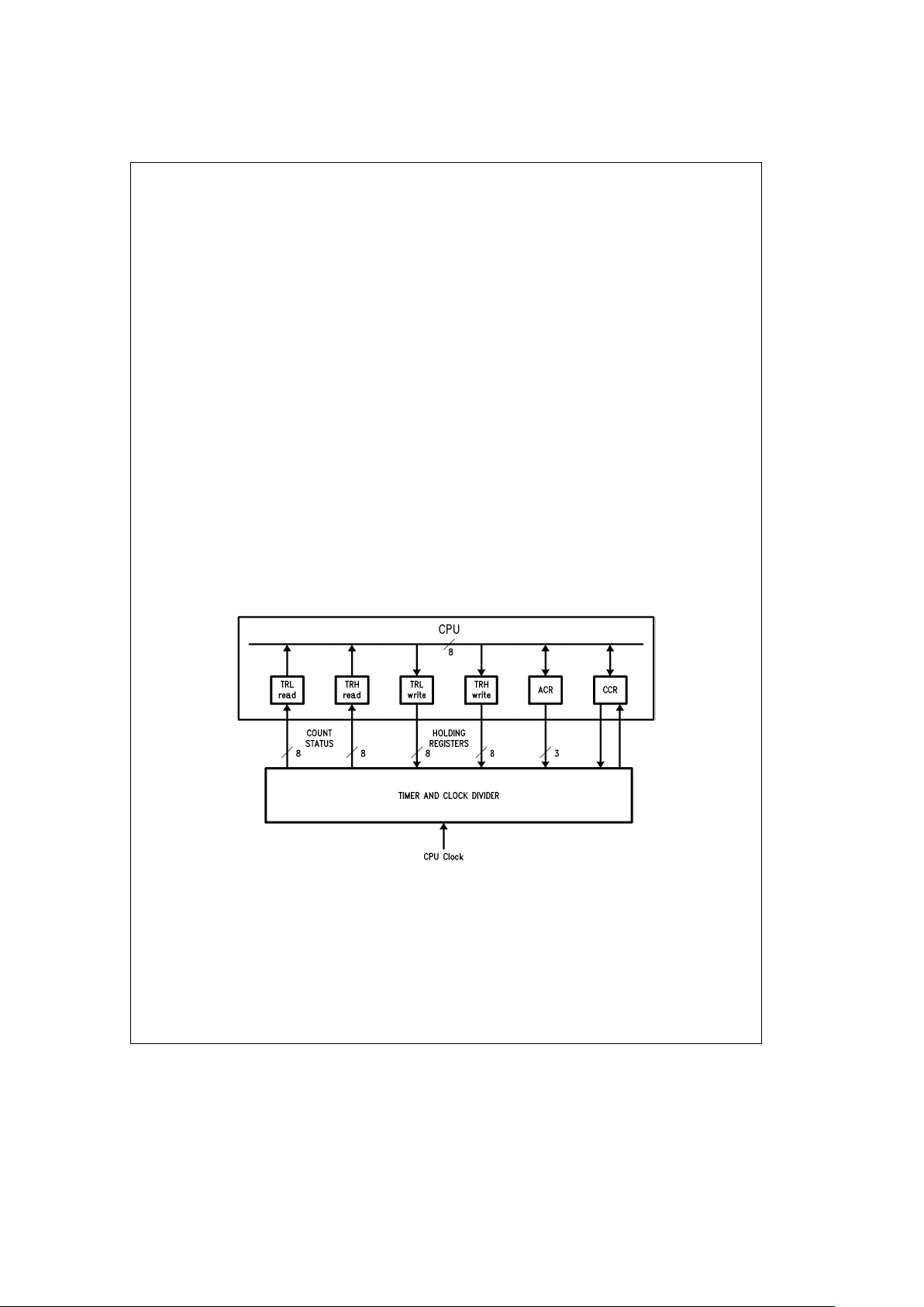
The timer block interfaces with the CPU via two registers,
TimeR Low byte,
À
TRLÓ, and TimeR High byte,ÀTRHÓ,
which form the input/output ports to the timer. Writing to
À
TRLÓandÀTRHÓstores the low and high byte, respectively, of a 16-bit time-out value into two holding registers. The
word stored in the holding registers is the value that the
timer will be loaded with via[TLD]. Also, the timer will automatically reload this word upon timing out. Reading
À
TRL
Ó
andÀTRHÓprovides access to the count down status of the
timer.
Control of timer operation is maintained via three bits in the
Auxiliary Control Register
À
ACRÓ. Timer STart[TST], bit 7
in
À
ACRÓ, is the start/stop control bit. Writing a one to
[
TST]allows the timer to start counting down from its current value. When low, the timer stops and the timer interrupt
is cleared. Timer Load[TLD],bit6in
À
ACRÓ, is the load
control of the timer. After writing the desired values into
À
TRLÓandÀTRHÓ, writing a one to[TLD]will load the 16-bit
word in the holding registers into the timer and initialize the
timer clock to zero in preparation to start counting. Upon
completing the load operation,[TLD]is automatically
cleared. Timer Clock Selection[TCS],bit5in
À
ACRÓ, determines the clock frequency of the timer count down. When
low, the timer divides the CPU clock by sixteen to form the
clock for the down counter. When[TCS]is high, the timer
divides the CPU clock by two. The input clock to the timer is
the CPU clock and should not be confused with the oscillator clock, OCLK. The rate of the CPU clock will be either
equal to OCLK or one-half of OCLK depending on the value
of bit 7 in the Device Control Register,
À
DCRÓ.
When the timer reaches a count of zero, the timer interrupt
is generated, the Time Out flag,[TO], (bit 7 in the Condition
Code Register
À
CCRÓ), goes high, and the timer reloads the
16-bit word stored in the holding registers to recycle through
a count down. The timer interrupt and[TO]can be cleared
by either writing a one to[TO]in
À
CCRÓor stopping the
timer by writing a zero to[TST]in
À
ACRÓ. Refer to Section
2.1.2, Timer for more information on the timer operation.
2.1.1.5 Transceiver Registers
Two registers in the Alternate A bank initialize transceiver
functions. The Auxiliary Transceiver Register,
À
ATRÓ, specifies a station address used by the address recognition logic
within the transceiver when using the non-promiscuous
5250 and 8-bit protocol modes. In 5250 modes,
À
ATRÓalso
defines how long the TX-ACT pin stays asserted after the
end of a transmitted message. The Fill Bit Register,
À
FBRÓ,
specifies the number of optional fill bits inserted between
frames in a multiframe 5250 message.
À
ICRÓcontains the Receiver Interrupt Select bits,[RIS1,0].
These bits determine the receiver interrupt source selection.
The source may be either Receiver FIFO Full, Data Available, or Receiver Active.
The Receive/Transmit Register,
À
RTRÓ, is the input/output
port to both the transmitter and receiver FIFO’s. It appears
to the BCP CPU like any other register. The
À
RTRÓregister
provides the least significant eight bits of data in both received and transmitted messages.
The Transceiver Mode Register,
À
TMRÓ, contains bits used
to set the configuration of the transceiver. As long as the
Transceiver RESet bit,[TRES], is high, the transceiver remains in reset. Internal LOOP-back operation of the transceiver can be selected by asserting[LOOP]. The RePeat
ENable bit,[RPEN], allows the receiver to be active at the
same time as the transmitter. When the Receiver INvert bit,
[
RIN], is set, all data sent to the receiver is inverted. The
Transmitter INvert bit,[TIN], is analogous to[RIN]except it
is for the transmitter. The protocol that the transceiver is
using is selected with the Protocol Select bits,[PS2–0].
The Transceiver Command Register,
À
TCRÓ, controls the
workings of the transmitter. To generate 5.5 line quiesce
pulses at the start of a transmission rather than 5, the Advance Transmitter Active bit,[ATA], must be set high. Parity
is automatically generated on a transmission and the Odd
Word Parity bit,[OWP], determines whether that parity is
even or odd. Bits 2– 0 of
À
TCRÓmake up part of the Trans-
mitter FIFO[TF10–8]along with
À
RTRÓ. Whenever a write
is made to
À
RTRÓ,[TF10–8]are automatically pushed on
the FIFO with the 8 bits written to
À
RTRÓ.
Other bits inÀTCRÓcontrol the operation of the on-chip
receiver. The number of line quiesce bits the receiver must
detect to recognize a valid message is determined by the
Receive Line Quiesce bit,[RLQ]. The BCP has its own internal analog comparator, but an off-chip one may be connected to DATA-IN. The receiver source is determined by the
Select Line Receiver bit,[SLR]. To view transceiver errors
in the Error Code Register,
À
ECRÓ, the Select Error Codes,
[
SEC], bit in
À
TCRÓmust be set high. When[SEC]is high,
Alternate Bank B R4 is remapped from
À
RTRÓtoÀECRÓso
that
À
ECRÓcan be read.
15

2.0 CPU Description (Continued)
Just as[TF10–8]bits get pushed onto the transmitter FIFO
when a write to
À
RTRÓoccurs, the Receiver FIFO bits,
[
RF10–8], in the Transceiver Status Register,
À
TSRÓ, re-
flect the state of the top word of the receive FIFO.
À
TSR
Ó
also contains flags that show Transmit FIFO Full,[TFF],
Transmitter Active,[TA], Receiver Error,[RE], Receiver Active,[RA], and Data AVailable,[DAV]. These flags may be
polled to determine the state of the transceiver. For instance, during a Receiver Active interrupt, the BCP can query the[DAV]bit to determine whether data is ready in the
receiver FIFO yet.
The Error Code Register,
À
ECRÓ, contains flags for receiver
errors. As previously stated, the[SEC]bit in
À
TRCÓmust be
set high to read this register. Reading
À
ECRÓor resetting
the transceiver with[TRES]will clear all the errors that are
present. The receiver OVerFlow flag,[OVF], is set when the
receiver attempts to add another word to the FIFO when it is
full. If internally checked parity and parity transmitted with a
3270 message conflict, then the PARity error bit,[PAR],is
set high. The Invalid Ending Sequence bit,[IES],isset
when the ending sequence in a 3270, 3299, or 8-bit message is incorrect. When the expected mid-bit transition in
the Manchester waveform does not occur, a Loss of Mid-Bit
Transition occurs ([LMBT]). Finally, if the transmitter is activated while the receiver is active, the Receiver DISabled
while active flag,[RDIS], will be set unless[RPEN]is asserted.
The second register in Main A bank is called the Network
Command Flag register,
À
NCFÓ, and contains information
about the transceiver which is useful for polling the transceiver (during other tasks for example) to see if it needs
servicing. These flags include bits to indicate Transmit FIFO
Empty[TFE], Receive FIFO Full[RFF], Line Active[LA],
and a Line Turn Around[LTA].[LTA]indicates that a message has been received without error and a valid ending
sequence has occurred. These flags facilitate polling of the
transceiver section when transceiver interrupts are not
used. Also included in this register is a bit called[DEME
]
(Data Error/Message End). In 3270/3299 modes, this bit
indicates a mismatch between received and locally generated byte parity. In 5250 modes,[DEME]decodes an end of
message indicator (111 in the address field). Three other
bits: Received Auto Response[RAR], Acknowledge[ACK
]
and Poll[POLL]are decoded from a received message (at
the output of the receive FIFO) and are valid only in 3270/
3299 modes where response time is critical.
Section 3.0 Transceiver provides comprehensive coverage
of this on-chip peripheral.
2.1.1.6 Condition Codes/Remote Handshaking Register
The ALU condition codes are available in the Condition
Code Register
À
CCRÓ. The[Z]bit is set when a zero result
is generated by an arithmetic, logical, or shift instruction.
Similarly,[N]indicates the Negative result of the same operations. An oVerflow condition from an arithmetic instruction sets the[V]bit in
À
CCRÓ. The Carry bit[C]indicates a
carry or borrow result from an arithmetic instruction. See
Section 2.2.2, ALU for more information.
The Condition Code Register,
À
CCRÓ, also contains[BIRQ],
a status bit which reflects the logic level of the bidirectional
interrupt input pin BIRQ. Hence, this pin can be used as a
general purpose input/output port as well as a bidirectional
interrupt request as defined by bits in
À
ACRÓandÀICRÓ.Ifa
remote CPU is present and shares data memory (dual port
memory) with the BCP, handshaking can be accomplished
by using the two status bits in
À
CCRÓcalled[RR]and[RW],
which indicate Remote Read and Remote Write accesses,
respectively.
In
À
ACRÓ, a lock bit,[LOR], is available to lock out all host
accesses. When this bit is set, all host accesses are disabled. Locking out remote accesses is often done during
interrupts to ensure quick response times.
The Remote Interface Configuration register,
À
RICÓ,isnot
available to the BCP internally. The Remote Interface Reference section provides further detail on
À
RICÓand interfac-
ing a remote processor.
2.1.1.7 Index Registers
Four index registers called IW, IX, IY, and IZ provide 16-bit
addressing for both data memory and instruction memory.
Each of these index registers is actually a pair of 8-bit registers which are individually addressable just like any other
CPU register. They occupy register addresses R12 through
R19. Thus, the first two pointers IW and IX (comprising
R12–R15) can be accessed with immediate mode instructions (which can access only R0 to R15). Refer to Section
2.1.3.2, Addressing Modes to see how the index registers
are formed from R12 –R19.
Accessing data memory requires the use of one of the four
index registers. All such instructions allow you to specify
which pointer is to be used, except the immediate-relative
moves: MOVE rs,[IZ
a
n]and MOVE[IZan],rd. These instructions always use the IZ pointer. Register indirect operations have options to alter the value of the index register;
the options include pre-increment, post-increment, and
post-decrement. These options facilitate block moves,
searches, etc. Refer to Section 2.1.3, Instruction Set for
more information about data moves.
Since the BCP’s ALU is 8 bits wide, all code that manipulates the index registers must act on them eight bits at a
time.
The index registers can also be used in register indirect
jumps (LJMP[Ir]), useful in implementing relocatable code.
Any one of the index registers can be specified to provide
the 16-bit instruction address for the indirect jump.
2.1.1.8 Stack Registers
The last two register addresses (R30,R31) are dedicated to
provide access to the two on-chip stacksÐthe data stack
and the address stack. The data stack is 8 bits wide and 16
words deep. It is a Last In First Out (LIFO) type and provides
high speed storage for variables, pointers, etc. The address
stack is 23 bits wide and 12 words deep, providing twelve
levels of nesting of subroutines and interrupts. It is also a
LIFO structure and stores processor status as well as return
addresses from CALL instructions, TRAP instructions, and
interrupts. The seven bits of processor status consist of the
four ALU flags, ([C],[N],[V], and[Z]), the current bank
setting (two bits), and[GIE].
Stack pointers for both the on-chip stacks are provided in
R30, the Internal Stack Pointer register,
À
ISPÓ. The lower
four bits are the pointer for the data stack and the upper
four bits are the pointer for the address stack. Both internal
stacks are circular. For example if 16 bytes are written to
16
2.0 CPU Description (Continued)
the data stack, the next byte pushed will overwrite the first.
À
ISPÓcan be read and written to like any other register, but
after a write, the BCP must execute one instruction before
reading the stack whose pointer was modified.
The Data Stack register,
ÀDSÓ
, is the input/output port for
the data stack. This port is accessed like any other register,
but a write to it will ‘‘push’’ a byte onto the stack and a read
from it will ‘‘pop’’ a byte from the stack. The data stack
pointer is updated when a read or write of
ÀDSÓ
occurs.
Information bits in the instruction address stack are not
mapped into the CPU’s register space and, therefore, are
not directly accessible. A remote system running a monitor
program can access this information by forcing the BCP to
single-step through a return instruction and then reading the
program counter. Since the stack pointers are writeable, the
remote system can access any location (return address) in
the address stack to trace program flow and then restore
the stack pointer to its original position.
2.1.2 Timer
The BCP has an internal 16-bit timer that can be used in a
variety of ways. The timer counts independently of the CPU,
eliminating the waste of valuable processor bandwidth. The
timer can be used in a polled or interrupt driven configuration for user software flexibility.
The timer interfaces with the CPU via two registers, TimeR
Low byte,
À
TRLÓ, and TimeR High byte,ÀTRHÓ, which form
the input/output ports to the timer. Writing to
À
TRLÓand
À
TRHÓstores the low and high byte, respectively, of a 16-bit
time-out value into two holding registers. The word stored in
the holding registers is the value that the timer will be load-
ed with via[TLD]. Also, the timer will automatically reload
this word upon timing out. Reading
À
TRLÓandÀTRHÓpro-
vides access to the count down status of the timer.
Control of timer operation is maintained via three bits in the
Auxiliary Control Register
À
ACRÓ. Timer STart[TST], bit 7
in
À
ACRÓ, is the start/stop control bit. Writing a one to
[
TST]allows the timer to start counting down from its current value. When low, the timer stops and the timer interrupt
is cleared. Timer Load[TLD],bit6in
À
ACRÓ, is the load
control of the timer. After writing the desired values into
À
TRLÓandÀTRHÓ, writing a one to[TLD]will load the 16-bit
word in the holding registers into the timer and initialize the
timer clock to zero in preparation to start counting. Upon
completing the load operation,[TLD]is automatically
cleared. Timer Clock Selection[TCS],bit5in
À
ACRÓ, determines the clock frequency of the timer count down. When
low, the timer divides the CPU clock by sixteen to form the
clock for the down counter. When[TCS]is high, the timer
divides the CPU clock by two. The input clock to the timer is
the CPU clock and should not be confused with the oscillator clock, OCLK. The rate of the CPU clock will be either
equal to OCLK or one-half of OCLK depending on the value
of bit 7 in the Device Control Register,
À
DCRÓ.
When the timer reaches a count of zero, the timer interrupt
is generated, the Time Out flag,[TO], (bit 7 in the Condition
Code Register
À
CCRÓ), goes high, and the timer reloads the
16-bit word stored in the holding registers to recycle through
a count down. The timer interrupt and[TO]can be cleared
by either writing a one to[TO]in
À
CCRÓor stopping the
timer by writing a zero to[TST]in
À
ACRÓ. A block diagram
of the timer is shown in
Figure 2-2.
TL/F/9336– D1
FIGURE 2-2. Timer Block Diagram
17

2.0 CPU Description (Continued)
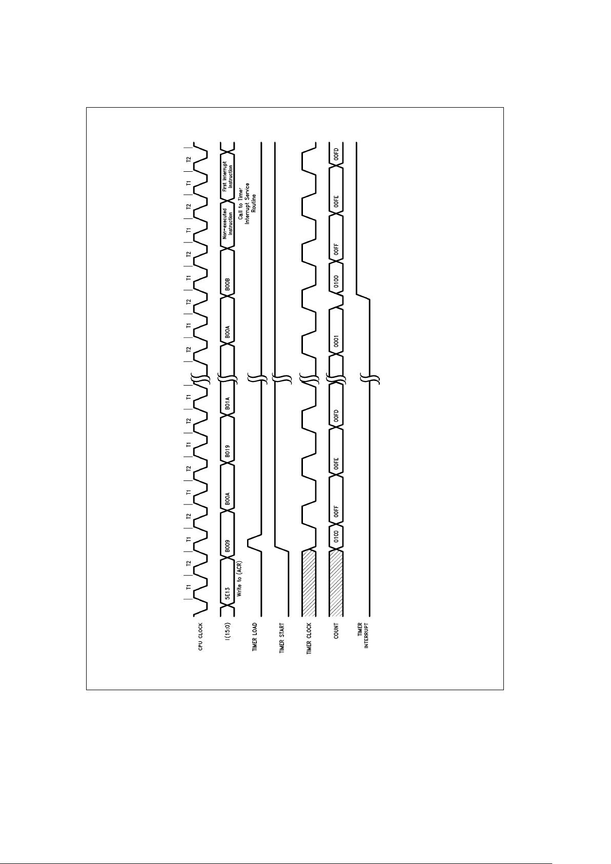
2.1.2.1 Timer Operation
After the desired 16-bit time-out value is written into
À
TRL
Ó
andÀTRHÓ, the start, load, and clock selection can be
achieved in a single write to
À
ACRÓ. A restriction exists on
changing the timer clock frequency in that[TCS]should not
be changed while the timer is running (i.e.,[TST]is high).
After a write to
À
ACRÓto load and start the timer, the timer
begins counting down at the selected frequency from the
value in
À
TRLÓandÀTRHÓ. Upon reaching a count of zero,
the timer interrupt is generated and, the timer reloads the
current word from
À
TRLÓandÀTRHÓto cycle through a
countdown again. The timing waveforms shown in
Figure
2-3
show a write toÀACRÓthat loads, starts, selects the
CPU clock rate/2 for the countdown rate, and asserts the
Global Interrupt Enable[GIE]. Prior to the write to
À
ACRÓ,
À
TRLÓandÀTRHÓwere loaded with 00h and 01h respectively, the timer interrupt was unmasked in the Interrupt
Control Register
À
ICRÓby clearing bit 4, and zero instruc-
tion wait states were selected in
À
DCRÓ. Since the write to
À
ACRÓasserted[GIE], the timer interrupt is enabled and
the CPU will vector to the timer interrupt service routine
address when the timer reaches a count of zero. The timer
interrupt is the lowest priority interrupt and is latched and
maintained until it is cleared in software. (See CPU Interrupts section). For very long time intervals, time-outs can be
accumulated under software control by writing a one to[TO
]
in
À
CCRÓallowing the timer to recycle its count down with
no other intervention. For time-outs attainable with one
count down, stopping the timer will clear the interrupt and
[TO]
. When the timer interrupt is enabled, the call to the
interrupt service routine occurs at different instruction
boundaries depending on when the timer interrupt occurs in
the instruction cycle. If the timer times out prior to T2, where
T2 is the last T-state of an instruction cycle, the call to the
interrupt service routine will occur in the next instruction.
When the time-out occurs in T2, the call to the interrupt
service routine will not occur in the next instruction. It occurs
in the second instruction following T2.
The count status of the timer can be monitored by reading
À
TRLÓand/orÀTRHÓ. When the registers are read, the output of the timer, not the value in the input holding registers,
is presented to the ALU. Some applications might require
monitoring the count status of the timer while it is counting
down. Since the timer can time-out between reads of
À
TRL
Ó
andÀTRHÓ, the software should take this fact into consideration. To read back what was written to
À
TRLÓandÀTRHÓ,
the timer must first be loaded via[TLD]without starting the
timer followed by a one instruction delay before reading
À
TRLÓandÀTRHÓto allow the output registers to be updat-
ed from the load operation.
To determine the time-out delay for a given value in
À
TRL
Ó
andÀTRHÓother than 0000h, the following equation can be
used:
TD
e
(value inÀTRHÓÀTRLÓ) * T * k
where:
ke2 when[TCS
]
e
1 or 16 when[TCS
]
e
0
TeThe period of the CPU clock
TD
e
The amount of time delay after the end of the in-
struction that asserts[TST]in
À
ACR
Ó
When the value of 0000h is loaded in the timer, the maximum time-out is obtained and is calculated as follows:
TD
e
65536 * T * k
With the CPU running full speed with an 18.8 MHz crystal,
the maximum single loop time delay attainable would be
55.6 ms ([TCS
]
e
0). The minimum time delay with the
same constraints is 106 ns ([TCS
]
e
1). For accumulating
time-out intervals, the total time delay is simply the number
of loops accumulated multiplied by the calculated time delay. The equations above do not account for any overhead
for processing the timer interrupt. The added overhead of
processing the interrupt may need to be included for precision timing.
18
2.0 CPU Description (Continued)
TL/F/9336– D2
FIGURE 2-3. Timer Interrupt Diagram
19

2.0 CPU Description (Continued)
2.1.3 Instruction Set
The followng paragraphs introduce the BCP’s architecture
by discussing addressing modes and briefly discussing the
Instruction Set. For detailed explanations and examples of
each instruction, refer to the Instruction Set Reference Section.
2.1.3.1 Harvard Architecture Implications
The BCP utilizes a true Harvard Architecture, where the instruction and data memory are organized into two independent memory banks, each with their own address and data
buses. Both the Instruction Address Bus and the Instruction
Bus are 16 bits wide with the Instruction Address Bus addressing memory by words. (A word of memory is 16 bits
long; i.e., 1 word
e
2 bytes.) Most of the instructions are
one word long. The exceptions are two words long, containing a word of instruction followed by a word of immediate
data. The combination of word sized instructions and a word
based instruction address bus eliminates the typical instruction alignment problems faced by many CPU’s.
The Data Address Bus is 16 bits wide (with the low order 8
bits multiplexed on the Data Bus), and the Data Bus is 8 bits
wide (i.e., one byte wide). The Data Address Bus addresses
memory by bytes. Most of the BCP’s instructions operate on
byte-sized operands.
Note that although both instruction addresses and data addresses are 16 bits long, these addresses are for two different buses and, therefore, have two different numerical
meanings, (i.e., byte address or word address.) Each instruction determines whether the meaning of a 16-bit address is that of an instruction word address or a data byte
address. Little confusion exists though because only the
program flow instructions interpret 16-bit addresses as instruction addresses.
2.1.3.2 Addressing Modes
An addressing mode is the mechanism by which an instruction accesses its operand(s). The BCP’s architecture supports five basic addressing modes: register, immediate, indexed, immediate-relative, and register-relative. The first
two allow instructions to execute the fastest because they
require no memory access beyond instruction fetch. The
remaining three addressing modes point to data or instruction memory. Typical of a RISC processor, most of the instructions only support the first three addressing modes,
with one of the operands always limited to the register addressing mode.
Register Addressing Modes
There are two terminologies for the register addressing
modes: Register and Limited Register. Instructions that allow Register operands can access all the registers in the
CPU. Note that only 32 of the 44 CPU registers are available
at any given point in time because the lower 12 register
locations (R0 –R11) access one of two switchable register
banks each. (See Section 2.1.1.1, Banked Registers for
more information on the CPU register banks.) Instructions
that allow the Limited Register operands can access just
the first 28 registers of the CPU. Again, note that only 16 of
these 28 registers are available at any given point in time.
Table 2-1 shows the notations used for the Register and
Limited Register operands. Some instructions also imply the
use of certain registers, for example the accumulators. This
is noted in the discussions of those instructions.
Immediate Addressing Modes
The two types of the immediate addressing modes available
are: Immediate numbers and Absolute numbers. Immediate
numbers are 8 bits of data, (one data byte), that code directly into the instruction word. Immediate numbers may represent data, data address displacements, or relative instruction addresses. Absolute numbers are 16-bit numbers. They
code into the second word of two word instructions and they
represent absolute instruction addresses. Table 2-2 shows
the notations used for both of these addressing modes.
TABLE 2-1. Register Addressing Mode Notations
Notation Type of Register Operand Registers Allowed
Rs Source Register R0–R31
Rd Destination Register R0–R31
Rsd Register is both a Source & Destination R0–R31
rs Limited Source Register R0–R15
rd Limited Destination Register R0–R15
rsd Limited Register is both a Source & Destination R0–R15
TABLE 2-2. Immediate Addressing Mode Notations
Notation Type of Immediate Operand Size
n Immediate Number 8 Bits
nn Absolute Number 16 Bits
20
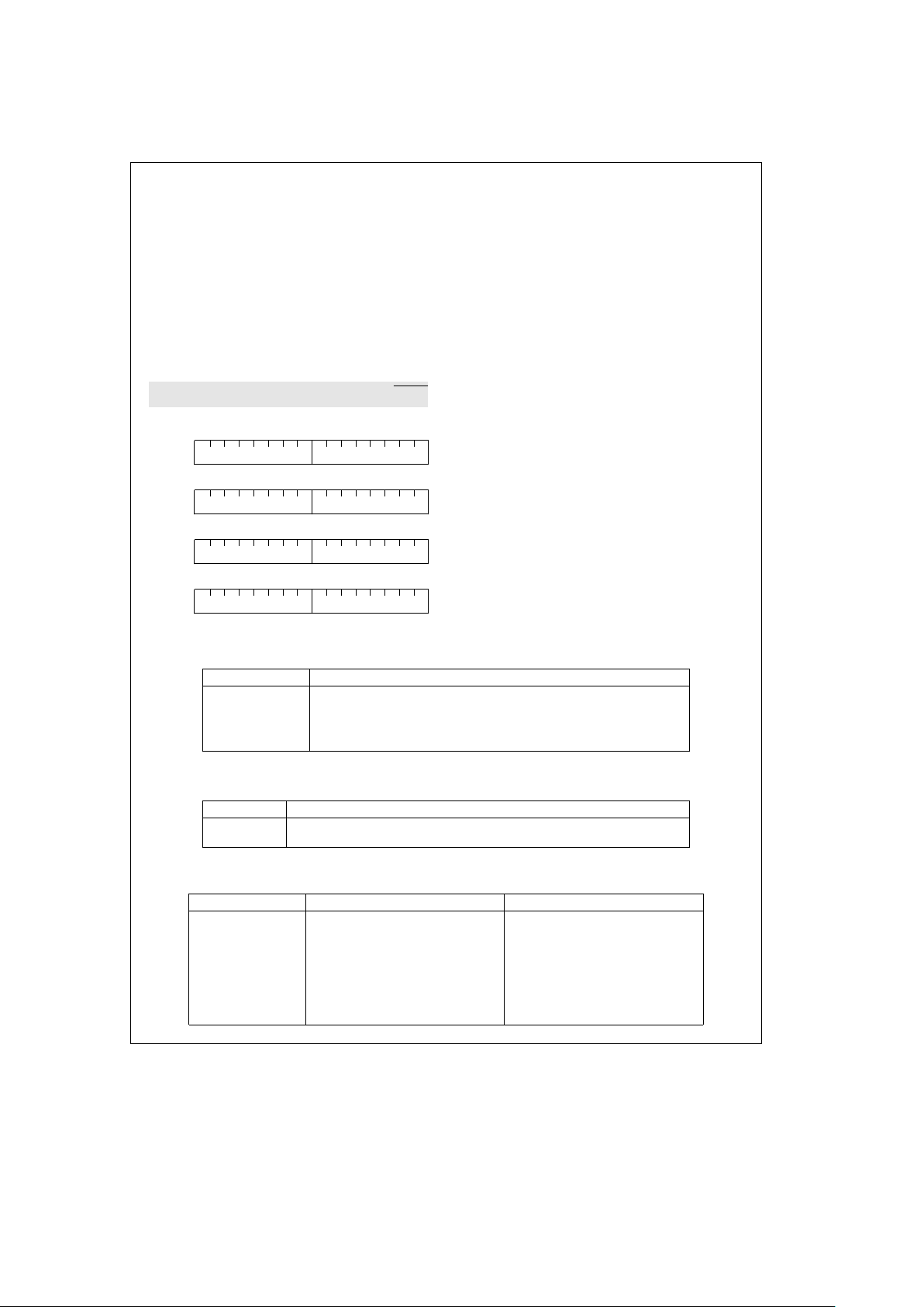
2.0 CPU Description (Continued)
Indexed Addressing Modes
Indexed operands involve one of four possible CPU register
pairs referred to as the index registers.
Figure 2-4
illustrates
how the index registers map into the CPU Register Set.
Note that the index registers are 16 bits wide.
Index registers allow for indirect memory addressing and
usually contain data memory addresses, although, the
LJMP instruction can use index registers to hold instruction
memory addresses. Most of the instructions that allow
memory indirect addressing, (i.e. the use of index registers),
also allow pre-incrementing, post-incrementing, or post-decrementing of the index register contents during instruction
execution, if desired. Table 2-3 lists the notations used for
the index register modes.
The index registers are set to zero when the BCP’s RESET
pin is asserted.
Index CPU Register Pair Forming Index Register
Register (MSB) (LSB)
IW R13 R12
15 8 7 0
IX R15 R14
15 8 7 0
IY R17 R16
15 8 7 0
IZ R19 R18
15 8 7 0
FIGURE 2-4. Index Register Map
Immediate-Relative and Register-Relative
Address Modes
The Immediate-Relative mode adds an unsigned 8-bit immediate number to the index register IZ forming a data byte
address. The Register-Relative mode adds the unsigned
8-bit value in the current accumulator, A, to any one of the
index registers forming a data byte address. Both of these
indirect memory addressing modes are available only on the
MOVE instruction. Table 2-4 shows the notation used for
these two addressing modes.
2.1.3.3 Instruction Set Overview
The BCP’s RISC instruction set contains seven categories
of instructions: Data Movement, Integer Arithmetic, Logic,
Shift-Rotate, Comparison, Program Flow, and Miscellaneous.
Data Movement Instructions
The MOVE instruction is responsible for all the data transfer
operations that the BCP can perform. Moving one byte at a
time, five different types of transfer are allowed: register to
register, data memory to register, register to data memory,
instruction memory to register, and instruction memory to
data memory. Table 2-5 lists all the variations of the MOVE
instruction.
TABLE 2-3. Index Register Addressing Mode Notations
Notation Meaning
[Ir]
Index Register, Contents Not Changed
[
Ir
b
]
Index Register, Contents Post-Decremented
[
Ir
a
]
Index Register, Contents Post-Incremented
[
a
Ir
]
Index Register, Contents Pre-Incremented
[
mIr
]
General Notation Indicating that Any of the Above Modes Is Allowed
Note:[]denotes indirect memory addressing and is part of the instruction syntax.
TABLE 2-4. Relative Index Register Mode Notations
Notation Type of Action Performed to Calculate a Data Memory Address
[
IZ
a
n
]
IZaImmediate Number (unsigned)xData Memory Address
[
Ir
a
A
]
Index RegisteraCurrent Accumulator (unsigned)xData Memory Address
Note:[]denotes indirect memory addressing and is part of the instruction syntax.
TABLE 2-5. Data Movement Instructions
Syntax Instruction Operation Addressing Modes
MOVE Rs, Rd registerxregister Register, Register
MOVE Rs,[mIr
]
register
x
data memory Register, Indexed
MOVE[mIr], Rd data memory
x
register Indexed, Register
MOVE Rs,[Ir
a
A
]
registerxdata memory Register, Register-Relative
MOVE[Ir
a
A], Rd data memoryxregister Register-Relative, Register
MOVE rs,[IZ
a
n
]
registerxdata memory Limited Register, Immediate-Relative
MOVE[IZ
a
n], rd data memoryxregister Immediate-Relative, Limited Register
MOVE n, rd instruction memoryxregister Immediate, Limited Register
MOVE n,[Ir
]
instruction memory
x
data memory Immediate, Indexed
21

2.0 CPU Description (Continued)
Integer Arithmetic Instructions
The integer arithmetic instructions operate on 8-bit signed
(two’s complement) binary numbers. Two arithmetic functions are supported: Add and Subtract. Three versions of
the Add and Subtract instructions exist: operand
g
accumu-
lator, operand
g
accumulatorgcarry, and immediate oper-
and
g
operand. The first two versions support both the register and indexed addressing modes for the destination operand. These two versions also allow the specification of a
separate register or data address for the destination operand so that the sources may retain their integrity; (i.e., true
three-operand instructions). Note that the currently active
‘‘B’’ register bank selects which accumulator is used in
these instructions. The third version, immediate operand
g
operand, only supports the register addressing mode for the
destination operand with the register as both a source and
the destination. Table 2-6 lists the integer arithmetic instructions along with their variations.
Logic Instructions
The logic instructions operate on 8-bit binary data. A full set
of logic functions is supported by the BCP: AND, OR, eXclusive OR, and Complement. All the logic functions except
complement allow either an immediate operand or the currently active accumulator as an implied operand. Complement only allows one register operand which is both the
source and destination. The other logic instructions include
the following addressing modes: register, indexed, and immediate. As with the integer arithmetic instructions, the integrity of the sources may be maintained by specifying a
destination register which is different from the source. Table
2-7 lists all the logic instructions.
TABLE 2-6. Integer Arithmetic Instructions
Syntax Instruction Operation Addressing Modes
ADD n, rsd registeranxregister Immediate, Limited Register
ADDA Rs, Rd Rs
a
accumulatorxRd Register, Register
ADDA Rs,[mlr
]
Rs
a
accumulatorxdata memory Register, Indexed
ADCA Rs, Rd Rs
a
accumulatoracarryxRd Register, Register
ADCA Rs,[mlr
]
Rs
a
accumulatoracarryxdata memory Register, Indexed
SUB n, rsd register
b
nxregister Immediate, Limited Register
SUBA Rs, Rd RsbaccumulatorxRd Register, Register
SUBA Rs,[mlr
]
Rs
b
accumulatorxdata memory Register, Indexed
SBCA Rs, Rd Rs
b
accumulatorbcarryxRd Register, Register
SBCA Rs,[mlr
]
Rs
b
accumulatorbcarryxdata memory Register, Indexed
TABLE 2-7. Logic Instructions
Syntax Instruction Operation Addressing Modes
AND n, rsd register & nxregister Immediate, Limited Register
ANDA Rs, Rd Rs & accumulator
x
Rd Register, Register
ANDA Rs,[mlr
]
Rs & accumulator
x
data memory Register, Indexed
OR n, rsd register
l
nxregister Immediate, Limited Register
ORA Rs, Rd Rs
l
accumulatorxRd Register, Register
ORA Rs,[mlr
]
Rs
l
accumulatorxdata memory Register, Indexed
XOR n, rsd registerZnxregister Immediate, Limited Register
XORA Rs, Rd Rs
Z
accumulatorxRd Register, Register
XORA Rs,[mlr
]
Rs
Z
accumulatorxdata memory Register, Indexed
CPL Rsd register
x
register Register
Note: &elogical AND operation
l
e
logical OR operation
Z
e
logical exclusive OR operation
r
e
one’s complement
22
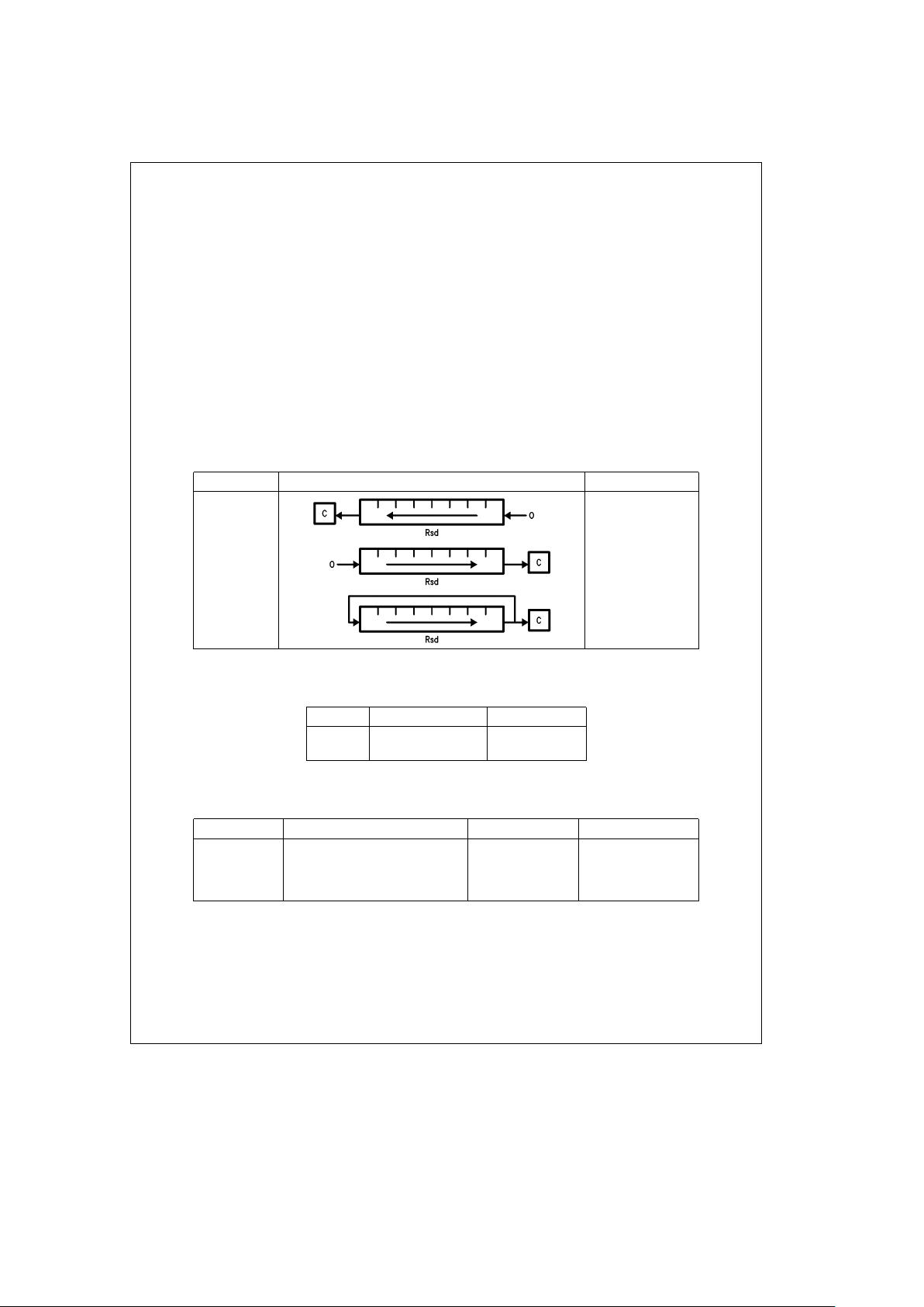
2.0 CPU Description (Continued)
Shift and Rotate Instructions
The shift and rotate instructions operate on any of the 8-bit
CPU registers. The BCP supports shift left, shift right, and
rotate operations. Table 2-8 lists the shift and rotate instructions.
Comparison Instructions
The BCP utilizes two comparison instructions. The CMP instruction performs a two’s complement subtraction between
a register and immediate data. The BIT instruction tests selected bits in a register by ANDing it with immediate data.
Neither instruction stores its results, only the ALU flags are
affected. Table 2-9 lists both of the comparison instructions.
Program Flow Instructions
The BCP has a wide array of program flow instructions: unconditional jumps, calls and returns; conditional jumps,
calls, and returns; relative or absolute instruction addressing
on jumps and calls; a specialized register field decoding
jump; and software interrupt capabilities. These instructions
redirect program flow by changing the Program Counter.
The unconditional jump instructions support both relative instruction addressing, the (JuMP instruction), and absolute
instruction addressing, (the Long JuMP instruction), using
the following addressing modes: Immediate, Register, Absolute, and Indexed. Table 2-10 lists the unconditional jump
instructions and their variations.
The conditional jump instructions support both relative instruction addressing and absolute instruction addressing using the Immediate and Absolute addressing modes. The
conditional relative jump instruction tests flags in the Condition Code Register,
À
CCRÓ, and the Transceiver Status
Register,
À
TSRÓ. Two possible syntaxes are supported for
the conditional relative jump instruction; see Table 2-11.
Table 2-12 lists the various flags ‘‘f’’ that the conditional
JMP instruction can test and Table 2-13 lists the various
conditions ‘‘cc’’ that the Jcc instruction can test for. Keep in
TABLE 2-8. Shift and Rotate Instructions
Syntax Instruction Operation Addressing Mode
SHL Rsd,b Register
SHR Rsd,b Register
ROT Rsd,b Register
Note: ‘‘b’’ethe number of bit shifts/rotates to perform.
TABLE 2-9. Comparison Instructions
Syntax Instruction Operation Addressing Mode
CMP rs, n registerbn Limited Register
BIT rs, n register & n Limited Register
Note: &elogical AND operation
TABLE 2-10. Unconditional Jump Instructions
Syntax Instruction Operation Operand Range Addressing Mode
JMP n PCan (sign extended)xPC
b
128,a127 Immediate
JMP Rs PC
a
Rs (sign extended)xPC
b
128,a127 Register
LJMP nn nn
x
PC 0, 64k Absolute
LJMP[Ir
]
Ir
x
PC 0, 64k Indexed
Note: PCeProgram Counter; contents initially points to instruction following jump.
23

2.0 CPU Description (Continued)
mind that the Jcc instruction is just an optional syntax for
the conditional JMP instruction.
The example in
Figure 2-5
demonstrates two possible ways
to code the conditional relative jump instruction when testing for a false[Z]flag in
À
CCRÓ. In the example, assume
that the symbol ‘‘Z’’ equals ‘‘000’’ binary, that the symbol
‘‘NS’’ equals ‘‘0’’ binary, and that the symbol ‘‘SKIP.IT’’
points to the desired instruction with which to begin execution if[Z]is false.
On the other hand, the conditional absolute jump instruction, LJMP, can test any bit in any currently active CPU register. Table 2-14 shows the conditional long jump instruction
syntax.
JMP Z,NS,SKIP.IT ;If[Z]40 goto SKIP.IT
-or-
JNZ SKIP.IT ;If[Z]40 goto SKIP.IT
FIGURE 2-5. Coding Examples of Equivalent
Conditional Jump Instructions
TABLE 2-11. Conditional Relative Jump Instruction
Syntax Instruction Operation Operand Range Addressing Mode
JMP f,s,n If the flag ‘‘f’’ is in the state ‘‘s’’
b
128,a127 Immediate
then PC
a
n (sign extended)xPC
Jcc n If the condition ‘‘cc’’ is met
b
128,a127 Immediate
then PC
a
n (sign extended)xPC
Note: PCeProgram Counter; contents initially points to instruction following jump.
TABLE 2-12. ‘‘f’’ Flags
‘‘f’’(Binary) Flag Flag Name
Register
Containing Flag
000 Z Zero
À
CCR
Ó
001 C Carry
À
CCR
Ó
010 V Overflow
À
CCR
Ó
011 N Negative
À
CCR
Ó
100 RA Receiver Active
À
TSR
Ó
101 RE Receiver Error
À
TSR
Ó
110 DAV Data Available
À
TSR
Ó
111 TFF Transmitter FIFO Full
À
TSR
Ó
TABLE 2-13. ‘‘cc’’ Conditions Tested
‘‘cc’’ Field Condition Tested for Flag ‘‘f’’’s Condition
Z Zero
[Z]
e
1
NZ Not Zero
[Z]
e
0
EQ Equal
[Z]
e
1
NEQ Not Equal
[Z]
e
0
C Carry
[C]
e
1
NC No Carry
[C]
e
0
V Overflow
[V]
e
1
NV No Overflow
[V]
e
0
N Negative
[N]
e
1
P Positive
[N]
e
0
RA Receiver Active
[RA]
e
1
NRA Not Receiver Active
[RA]
e
0
RE Receiver Error
[RE]
e
1
NRE No Receiver Error
[RE]
e
0
DA Data Available
[
DAV
]
e
1
NDA No Data Available
[
DAV
]
e
0
TFF Transmitter FIFO FULL
[
TFF
]
e
1
NTFF Transmitter FIFO Not Full
[
TFF
]
e
0
TABLE 2-14. Conditional Absolute Jump Instruction
Syntax Instruction Operation Operand Range Addressing Mode
LJMP Rs,p,s,nn If the bit of register ‘‘Rs’’ in 0, 64k Register, Absolute
position ‘‘p’’ is in the state ‘‘s’’
then nn
x
PC
Note: PCeProgram Counter
24

2.0 CPU Description (Continued)
The BCP also has a specialized relative jump instruction
called relative Jump with Rotate and Mask on source register, JRMK. This instruction facilitates the decoding of register fields often involved in communications processing.
JRMK does this by rotating and masking a copy of its register operand to form a signed program counter displacement
which usually points into a jump table. Table 2-15 shows the
syntax and operation of the JRMK instruction.
JRMK’s masking, (setting to zero), the least significant bit of
the displacement allows the construction of a jump table
using either one or two word instructions; for instance, a
table of JMP and/or LJMP instructions, respectively. The
example in
Figure 2-6
demonstrates the JRMK instruction
decoding the address frame of the 3299 Terminal Multiplex-
er protocol which is located in the Receive/Transmit Register,
À
RTR[4–2
]
Ó
.
The BCP has two unconditional call instructions; CALL,
which supports relative instruction addressing and LCALL,
(Long CALL), which supports absolute instruction addressing. These instructions push the following information onto
the CPU’s internal Address Stack: the address of the next
instruction; the status of the Global Interrupt Enable flag,
[
GIE]; the status of the ALU flags[Z],[C],[N], and[V]; and
the status of which register banks are currently active. Table
2-16 lists the two unconditional call instructions. Note that
the Address Stack is only twelve positions deep; therefore,
the BCP allows twelve levels of nested subroutine invocations, (this includes both interrupts and calls).
TABLE 2-15. JRMK Instruction
Syntax Instruction Operation
Displacement
Addressing Mode
Range
JRMK Rs, b, m (a) Rotate a copy of register ‘‘Rs’’ ‘‘b’’ bits to the right.
b
128,a126 Register
(b) Mask the most significant ‘‘m’’ bits and the least
significant bit of the above result.
(c) PC
a
resulting displacement (sign extended)xPC.
Note: PCeProgram Counter; contents initially points to instruction following jump.
Example Code
JRMK RTR,1,4 ;decode terminal address
LJMP ADDR.0 ;jump to device handler #0
LJMP ADDR.1 ;jump to device handler #1
...
LJMP ADDR.7 ;jump to device handler #7
Instruction Execution JRMK Displacement Register Contents
(a) Copy
À
RTRÓinto JRMK’s displacement register: x x x A2 A1 A0 y y
(b) Rotate displacement register 1 bit to the right: y x x x A2 A1 A0 y
(c) AND result with ‘‘00001110’’ binary mask: 0 0 0 0 A2 A1 A0 0
(d) Sign extend resulting displacement and add
it to the program counter, (PC).
If the bits A2 A1 A0 equal ‘‘0 0 1’’ binary then
a
2 is added to the Program Counter; 0 0 0 0 0 0 1 0
(i.e., PC
a
2xPC).
(e) Execute the instruction pointed to by the PC,
which in this example is:
LJMP ADDR.1
FIGURE 2-6. JRMK Instruction Example
TABLE 2-16. Unconditional Call Instructions
Syntax Instruction Operation
Operand
Addressing Mode
Range
CALL n PC &[GIE]& ALU flags & reg. bank selectionxAddress Stackb128,a127 Immediate
PC
a
n (sign extended)xPC
LCALL nn PC &[GIE]& ALU flags & reg. bank selection
x
Address Stack 0, 64k Absolute
nn
x
PC
Note: PCeProgram Counter; contents initially points to instruction following call.
[
GIE
]
e
Global Interrupt Enable bit.
&
e
concatenation operator, combines operands together forming one long operand.
25

2.0 CPU Description (Continued)
The BCP has one conditional call instruction capable of
testing any bit in any currently active CPU register. This call
only supports absolute instruction addressing. Table 2-17
shows the conditional call instruction syntax and operation.
The return instruction complements the above call instructions. Two versions of the return instruction exist, the uncondtional return and the conditional return. When the unconditional return instruction is executed, it pops the last
address on the CPU’s Address Stack into the program
counter and it can optionally affect the[GIE]bit, the ALU
flags, and the register bank selection. Table 2-18 shows the
syntax and operation of the unconditional return instruction.
The conditional return instruction functions the same as the
unconditional return instruction if a desired condition is met.
As with the conditional jump instruction, the conditional return instruction has two possible syntaxes. Table 2-19 lists
the syntax for the conditional return. The ‘‘f’’ flags and the
‘‘cc’’ conditions for the return instruction are the same as
for the conditional jump instruction, therefore refer to Table
2-12 and Table 2-13 for the listing of ‘‘f’’ and ‘‘cc’’, respectively.
TABLE 2-17. Conditional Call Instruction
Syntax Instruction Operation Operand Range Addressing Mode
LCALL Rs, p, s, nn If the bit of register ‘‘Rs’’ in position 0, 64k Register, Absolute
‘‘p’’ is in the state ‘‘s’’ then
PC &[GIE]& ALU flags &
reg. bank selection
x
Address Stack
nn
x
PC
End if
Note: PCeProgram Counter; contents initially points to instruction following call.
[
GIE
]
e
Global Interrupt Enable bit
&
e
concatenation operator, combines operands together forming one long operand.
TABLE 2-18. Unconditional Return Instruction
Syntax Instruction Operation
RETÀgÀ,rfÓÓCase ‘‘g’’ of
0: leave[GIE]unaffected, (default)
1: restore[GIE]from Address Stack
2: set[GIE
]
3: clear[GIE
]
End case
If ‘‘rf’’e1 then
restore ALU flags from Address Stack
restore register bank selection from Address Stack
Else (the default)
leave the ALU flags and register bank selections unchanged
End if
Address Stack
x
PC
Note: PCeProgram Counter
[
GIE
]
e
Global Interrupt Enable bit
ÀÓ e
surrounds optional operands that are not part of the instruction syntax.
Optional operands may either be specified or omitted.
TABLE 2-19. Conditional Return Instruction
Syntax Instruction Operand
RETF f, sÀ,ÀgÓ,À,rf
ÓÓ
If the flag ‘‘f’’ is in the state ‘‘s’’ then perform a RETÀgÀ,rf
ÓÓ
Rcc
ÀgÀ
,rf
ÓÓ
If the condition ‘‘cc’’ is met then perform a RETÀgÀ,rf
ÓÓ
Note: See Table XVIII for an explanation of ‘‘RETÀgÀ,rfÓÓ’’
ÀÓ e
surrounds optional operands that are not part of the instruction syntax.
Optional operands may either be specified or omitted.
26
2.0 CPU Description (Continued)
In addition to the above jump, call and return program flow
instructions, the BCP is capable of generating software interrupts via the TRAP instruction. This instruction generates
a call to any one of 64 possible interrupt table addresses
based on its vector number operand. This allows both the
simulation of hardware interrupts and the construction of
special software interrupts, if desired. The actual interrupt
table entry address is determined by concatenating the Interrupt Base Register,
À
IBRÓ, to an 8-bit representation of
the vector number operand in the TRAP instruction. This
instruction may also clear the[GIE]bit, if desired. Table
2-20 shows the syntax and operation of the TRAP instruction.
Miscellaneous Instructions
As stated in the ‘‘CPU Register Set’’ section, the BCP has
44 registers with 24 of them arranged into four register
banks: Main Bank A, Alternate Bank A, Main Bank B, and
Alternate Bank B. The exchange instruction, EXX, selects
which register banks are currently available to the CPU, for
example either Main Bank A or Alternate Bank A. The deselected register banks retain their current values. The EXX
instruction can also alter the state of[GIE], if desired. Table
2-21 shows the EXX instruction syntax and operation.
TABLE 2-20. TRAP Instruction
Syntax Instruction Operation Operand Range
TRAP vÀ,g
Ê
Ó
PC &[GIE]& ALU flags & 0, 63
reg. Bank Selection
x
Address Stack
If ‘‘g
Ê
’’e1 then clear[GIE
]
Form PC address as shown below:
Note: PCeProgram Counter; contents initially points to instruction following call.
[
GIE
]
e
Global Interrupt Enable bit
IBR
e
Interrupt Base Register
&
e
concatenation operator, combines operands together forming one long operand.
ÀÓe
surrounds optional operands that are not part of the instruction syntax.
Optional operands may either be specified or omitted.
TABLE 2-21. EXX Instruction
Syntax Instruction Operation
EXX ba, bbÀ,gÓCase ‘‘ba’’ of
0: activate Main Bank A
1: activate Alternate Bank A
End case
Case ‘‘bb’’ of
0: activate Main Bank B
1: activate Alternate Bank B
End case
Case ‘‘g’’ of
0: leave[GIE]unaffected, (default)
1: (reserved)
2: set[GIE
]
3: clear[GIE
]
End case
Note:[GIE
]
e
Global Interrupt Enable bit
ÀÓe
surrounds optional operands that are not part of the instruction syntax.
Optional operands may either be specified or omitted.
27
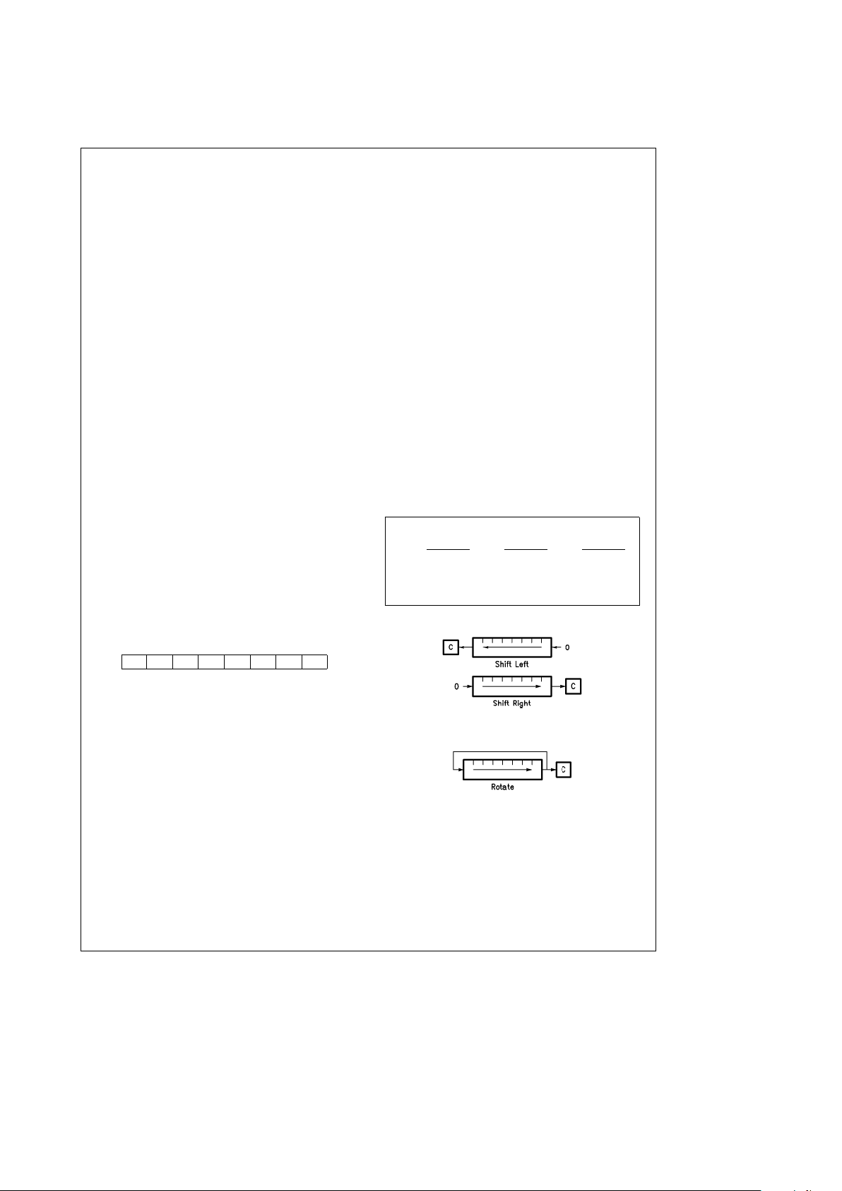
2.0 CPU Description (Continued)
2.2 CPU FUNCTIONAL DESCRIPTION
2.2.1 ALU
The BCP provides a full function high speed 8-bit Arithmetic
Logic Unit (ALU) with full carry look ahead, signed arithmetic, and overflow decision capabilities. The ALU can perform
six arithmetic, nine logic, one rotate and two shift operations
on binary data. Full access is provided to all CPU registers
as both source and destination operands, and using the indirect addressing mode, results may be placed directly into
data memory. All operations which have an internal destination (register addressing) are completed in two (2) T-states.
External destination operations (indirect addressing to data
memory) complete in three (3) T-states.
Arithmetic operations include addition with or without carry,
and subtraction with or without borrow (represented by carry). Subtractions are performed using 2’s complement addition to accommodate signed operands. The subtrahend is
converted to its 2’s complement equivalent by the ALU and
then added to the minuend. The result is left in 2’s complement form.
The remaining ALU operations include full logic, shift and
rotate operations. The logic functions include Complement,
AND, OR, Exclusive-OR, Compare and Bit Test. Zero
through seven bit right and left shift operations are provided,
along with a zero through seven bit right rotate operation.
Note that the shift and rotate operations may only be performed on a register, which is both the source and destination. (See the Instruction Set Overview section for detailed
descriptions of these operations.)
The BCP ALU provides the programmer with four instruction
result status bits for conditional operations. These bits
(known as condition code flags) indicate the status (or condition) of the destination byte produced by certain instructions. Not all instructions have an affect on every status flag.
(See the Instruction Set Reference section for the specific
details on what status flags a given instruction affects.)
These flags are held in the Condition Code Register,
À
CCRÓ, see
Figure 2-7.
76543210
TO RR RW BIRQ N V C Z
where:
NeNegative
C
e
Carry
VeOverflow
ZeZero
FIGURE 2-7. Condition Code Register ALU Flags
If an instruction is documented as affecting a given flag,
then the flags are set (to 1) or cleared (to 0) under the
following conditions:
[N]
Ð The Negative flag is set if the most significant bit
(MSB) of the result is one (1), otherwise it is cleared.
This flag represents the sign of the result if it is interpreted as a 2’s complement number.
[C]
Ð The Carry flag is set if:
a) An addition operation generates a carry, see
Fig-
ure 2-8a.
b) A subtract or compare operation generates a bor-
row, see
Figure 2-8b.
c) The last bit shifted out during a shift operation (in
either direction) is a one (1), see
Figure 2-9.
d) The last bit rotated by the rotate operation is a one
(1), see
Figure 2-10.
In all other conditions[C]is cleared.
[V]
Ð Overflow is set whenever the result of an arithmetic or
compare operation on signed operands is not representable by the operand size, thereby producing an
incorrect result. For example, the addition of the two
signed negative numbers in
Figure 2-8a
would set[V
]
since the correct representation of the result, both
sign and magnitude, is not possible in 8 bits. On the
other hand, in
Figure 2-8b
and
2-8c
[V]
would be
cleared because the results are correctly represented
in both sign and magnitude. It is important to remember that Overflow is only meaningful in signed arithmetic and that it is the programmer’s responsibility to
determine if a given operation involves signed or unsigned values.
[Z]
Ð The Zero flag is set only when an operation produces
an all bits cleared result (i.e., a zero). In all other conditions[Z]is cleared.
11101010 10111010 11011100
a
10001100
b
11000100
a
01100011
1w01110110 1x11110110 1w00111111
[C]
e
1
[C]
e
1
[C]
e
1
[V]
e
1
[V]
e
0
[V]
e
0
(a) (b) (c)
FIGURE 2.8. Carry and Overflow Calculations
TL/F/9336– D3
FIGURE 2-9. Shifts’ Effect on Carry
TL/F/9336– D4
FIGURE 2-10. Rotate’s Effect on Carry
28

2.0 CPU Description (Continued)
Several conditions apply to these flags, independent of their
operation and the way they are calculated. These conditions
are:
1. A flag’s previous state is retained when an instruction has
no affect on that flag.
2. Direct reading and writing of all ALU flags is possible via
the
À
CCRÓregister.
3. Currrent flag values are saved onto the address stack
during interrupt and call operations, and can be restored
to their original values if a return instruction with the restore flags option is executed.
4. Flag status is calculated in parallel with the instruction
result, therefore no time penalty is associated with flag
operation.
When performing single byte arithmetic (i.e., the values are
completely represented in one byte) the Add (ADD,ADDA)
and Subtract (SUB,SUBA) instructions should be used, but
when performing multi-byte arithmetic the Add with Carry
(ADCA) and Subtract with Carry (SBCA) instructions should
be used. This is because the carry (in an add operation) or
the borrow (in a subtract operation) must be carried forward
to the higher order bytes.
Figure 2-11
demonstrates an instruction sequence for a 16-bit add and an instruction sequence for a 16-bit subtract.
Assume the 16-bit variable X is represented by the register pair R4(MSB), R5(LSB), and that the 16-bit variable
Y is represented by the register pair R6(MSB), R7(LSB).
To perform the assignment Y
eXa
Y:
MOVE R7,A ;GET LSB OF Y
ADDA R5,R7 ;Y(LSB)4X(LSB)0Y(LSB)
MOVE R6,A ;GET MSB OF Y
ADCA R4,R6 ;Y(MSB)4X(MSB)0Y(MSB)
0CARRY
To perform the assignment YeX 1 Y:
MOVE R7,A ;GET LSB OF Y
SUBA R5,R7 ;Y(LSB)4X(LSB)1Y(LSB)
MOVE R6,A ;GET MSB OF Y
SBCA R4,R6 ;Y(MSB)4X(MSB)1Y(MSB)
1CARRY
FIGURE 2-11. Multi-Byte Arithmetic
Instruction Sequences
When using the ALU to perform comparisons, the programmer has two options. If the compare is to a constant value
then the CMP instruction can be used, else one of the subtract instructions must be used. When determining the results of any compare, the programmer must keep in mind
whether they are comparing signed or unsigned values. Table 2-22 lists the Boolean condition that must be met for
unsigned comparisons and Table 2-23 lists the Boolean
condition that must be met for signed comparisons.
TABLE 2-22
Unsigned Comparison Results
Comparison: xby Boolean Condition
xkyC
x
s
yC
l
Z
x
e
yZ
x
t
yC
x
l
yC&Z
Note: &elogical AND
l
e
logical OR
z
e
one’s complement
TABLE 2-23
Signed Comparison Results
Comparison: xby Boolean Condition
xky (N&V)l(N&V)
x
s
yZ
l
(N&V)l(N&V)
x
e
yZ
X
t
y (N&V)l(N&V)
xly (N&V&Z)l(N&V&Z)
Note: &elogical AND
l
e
logical OR
z
e
one’s complement
2.2.2 Timing
Timing on the BCP is controlled by an internal oscillator and
circuitry that generates the internal timing signals. This circuitry in the CPU is referred to as Timing Control. The internal timing of the CPU is synchronized to an internal clock
called the CPU clock, CPU-CLK. A period of CPU-CLK is
referred to as a T-state. The clock for the BCP is provided
by a crystal connected between X1 and X2 or from a clock
source connected to X1. This clock will be referred to as the
oscillator clock, OCLK. The frequency of OCLK is divided in
half when the CPU clock select bit,[CCS], in the Device
Control Register,
À
DCRÓ, is set to a one. Either OCLK or
OCLK/2 is used by Timing Control to generate CPU-CLK
and other synchronous signals used to control the CPU timing.
After the BCP is reset,[CCS]is high and CPU-CLK is generated from OCLK/2. Since the output of the divider that creates OCLK/2 can be high or low after reset, CPU-CLK can
also be in a high or low state. Therefore, the exact number
of clock cycles to the start of the first instruction cannot be
determined. Automatic test equipment can synchronize to
the BCP by asserting RESET
as shown in
Figure 2-12.
The
falling edge of RESET
generates a clear signal which causes CPU-CLK to fall. The next rising edge of X1 removes the
clear signal from CPU-CLK. The second rising edge of X1
will cause CPU-CLK to rise and the relationship between X1
and CPU-CLK can be determined from this point.
Writing a zero to[CCS]causes CPU-CLK to switch from
OCLK/2 to OCLK. The transition from OCLK to OCLK/2
occurs following the end of the instruction that writes to
29
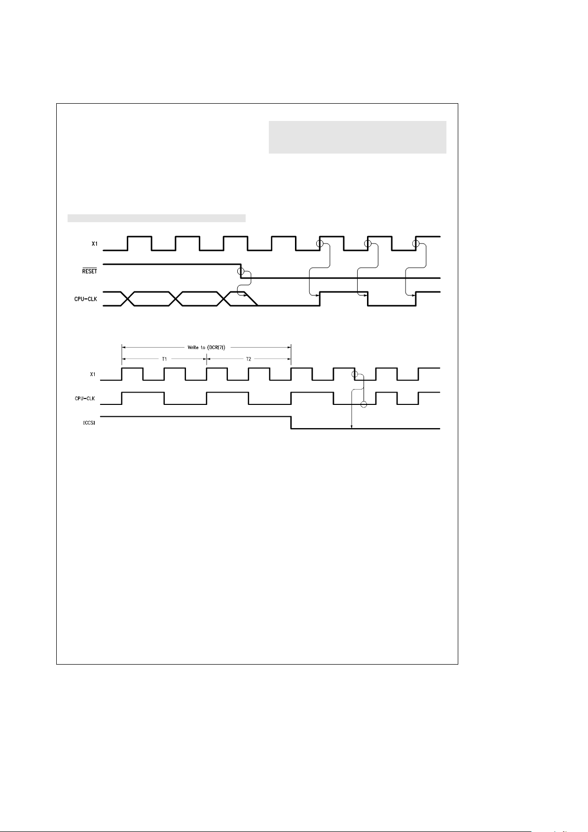
2.0 CPU Description (Continued)
[
CCS]as shown in
Figure 2-13.
The switch occurs on the
falling edge of X1 when CPU-CLK is low. CPU-CLK can be
changed back to OCLK/2 by writing a one to[CCS]. The
point at which CPU-CLK changes depends on whether
there has been an odd or even number of T-states since
[
CCS]was set low. The change would require a maximum
of two T-states and a minimum of one T-state following the
end of the instruction that writes to[CCS].
The CPU is a RISC processor with a limited number of instructions which execute in a short period of time. The maximum instruction cycle time is four T-states and the minimum
is two T-states. Six types of instruction timing are used in
the CPU: two T-state, three T-state program control, three
T-state data memory access, four T-state read data memory
access, four T-state program control, and four T-state two
word program control. The first T-state of each instruction
is T1 and the last T-state is T2. Intermediate T-states required to complete the instruction are referred to as TX.
The instruction clock output, ICLK, defines the instruction
boundaries. ICLK rises at the beginning of each instruction
and falls one-half T-state after the next address is generated on the instruction address bus, IA. Thus, ICLK indicates
the start of each instruction and when the next instruction
address is valid.
TL/F/9336– D5
FIGURE 2-12. CPU-CLK Synchronization with X1
TL/F/9336– D6
FIGURE 2-13. Changing from OCLK/2 to OCLK
30
 Loading...