

TL/F/11705
DP83266 MACSI Device (FDDI Media Access Controller and System Interface)
PRELIMINARY
October 1994
DP83266 MACSITMDevice
(FDDI Media Access Controller and System Interface)
General Description
The DP83266 Media Access Controller and System Interface (MACSI) implements the ANSI X3T9.5 Standard Media
Access Control (MAC) protocol for operation in an FDDI
token ring and provides a comprehensive System Interface.
The MACSI device transmits, receives, repeats, and strips
tokens and frames. It produces and consumes optimized
data structures for efficient data transfer. Full duplex architecture with through parity allows diagnostic transmission
and self testing for error isolation and point-to-point connections.
The MACSI device includes the functionality of both the
DP83261 BMAC
TM
device and the DP83265 BSI-2TMdevice
with additional enhancements for higher performance and
reliability.
Features
Y
Over 9 kBytes of on-chip FIFO
Y
5 DMA channels (2 Output and 3 Input)
Y
12.5 MHz to 25 MHz operation
Y
Full duplex operation with through parity
Y
Supports JTAG boundary scan
Y
Real-time Void stripping indicator for bridges
Y
On-chip address bit swapping capability
Y
32-bit wide Address/Data path with byte parity
Y
Programmable transfer burst sizes of 4 or 8
32-bit words
Y
Receive frame filtering services
Y
Frame-per-Page mode controllable on each
DMA channel
Y
Demultiplexed Addresses supported on ABus
Y
New multicast address matching feature
Y
ANSI X3T9.5 MAC standard defined ring
service options
Y
Supports all FDDI Ring Scheduling Classes
(Synchronous, Asynchronous, etc.)
Y
Supports Individual, Group, Short, Long and
External Addressing
Y
Generates Beacon, Claim, and Void frames
Y
Extensive ring and station statistics gathering
Y
Extensions for MAC level bridging
Y
Enhanced SBus compatibility
Y
Interfaces to DRAMs or directly to system bus
Y
Supports frame Header/Info splitting
Y
Programmable Big or Little Endian alignment
Block Diagram
TL/F/11705– 1
FIGURE 1-1. FDDI Chip Set Block Diagram
TRI-STATEÉis a registered trademark of National Semiconductor Corporation.
BMAC
TM
, BSI-2TM, MACSITMand PLAYER
a
TM
are trademarks of National Semiconductor Corporation.
C
1995 National Semiconductor Corporation RRD-B30M105/Printed in U. S. A.

Table of Contents
1.0 FDDI CHIP SET OVERVIEW
2.0 GENERAL FEATURES
2.1 FDDI MAC Support
2.2 MAC Addressing Support
2.3 MAC Bridging Support
2.4 MAC Service Class Support
2.5 Diagnostic Counters
2.6 Management Services
2.7 Ring Parameter Tuning
2.8 Multi-Frame Streaming Interface
2.9 Beacon, Claim and Void Frames Generation
2.10 Self Testing
2.11 32-Bit Address/Data Path to Host Memory
2.12 Multi-Channel Architecture
2.13 Support for Header/Info Splitting
2.14 MAC Bridging Support
2.15 Address Bit Swapping
2.16 Status Batching Services
2.17 Receive Frame Filtering Services
2.18 Two Timing Domains
2.19 Clustered Interrupts
2.20 FIFO Memory
2.21 Frame-per-Page-per-Channel
2.22 Copy All Multicast
2.23 Bridge Stripping Information
2.24 LED Status Control Outputs
2.25 JTAG Boundary Scan
3.0 ARCHITECTURAL DESCRIPTION
3.1 Interfaces
3.2 Ring Engine
3.3 Data Structures
3.4 Service Engine
4.0 FDDI MAC FACILITIES
4.1 Symbol Set
4.2 Protocol Data Units
4.3 Frame Counts
4.4 Timers
4.5 Ring Scheduling
5.0 FUNCTIONAL DESCRIPTION (RING ENGINE)
5.1 Token Handling
5.2 Servicing Transmission Requests
5.3 Request Service Parameters
5.4 Frame Validity Processing
5.0 FUNCTIONAL DESCRIPTION (RING ENGINE)
(Continued)
5.5 Frame Status Processing
5.6 SMT Frame Processing
5.7 MAC Frame Processing
5.8 Receive Batching Support
5.9 Immediate Frame Transmission
5.10 Full Duplex Operation
5.11 Parity Processing
5.12 Handling Internal Errors
6.0 FUNCTIONAL DESCRIPTION (SERVICE ENGINE)
6.1 Overview
6.2 Operation
6.3 External Matching Interface
6.4 Bus Interface Unit
6.5 Enhanced ABUS Mode
7.0 CONTROL INFORMATION
7.1 Overview
7.2 Conventions
7.3 Access Rules
7.4 Ring Engine Operation Registers
7.5 MAC Parameters
7.6 Timer Values
7.7 Event Counters
7.8 Pointer RAM Registers
7.9 Limit RAM Registers
7.10 Descriptors
7.11 Operating Rules
7.12 Pointer RAM Register Descriptions
7.13 Limit RAM Register Descriptions
8.0 SIGNAL DESCRIPTIONS
8.1 Control Interface
8.2 PHY Interface
8.3 External Matching Interface
8.4 LED Interface
8.5 ABus Interface
8.6 Electrical Interface
9.0 ELECTRICAL CHARACTERISTICS
9.1 Absolute Maximum Ratings
9.2 Recommended Operating Conditions
9.3 DC Electrical Characteristics
9.4 AC Electrical Characteristics
10.0 PIN TABLE AND PIN DIAGRAM
2

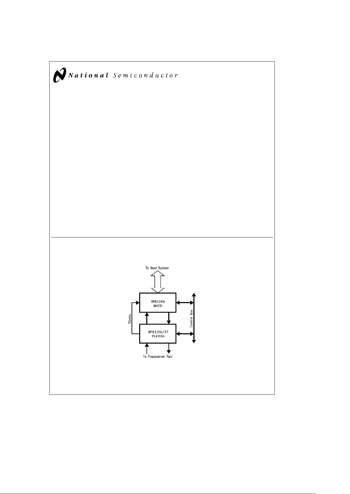
1.0 FDDI Chip Set Overview
National Semiconductor’s FDDI chip set is shown in
Figure
1-1.
For more information about the PLAYER
a
TM
device,
consult the appropriate datasheet and application notes.
DP83256/56-AP/57 PLAYER
a
Device Physical Layer Controller
The PLAYERadevice implements the Physical Layer
(PHY) protocol as defined by the ANSI FDDI PHY X3T9.5
Standard along with all the necessary clock recovery and
clock generation functions.
Features
#
Single chip FDDI Physical Layer (PHY) solution
#
Integrated Digital Clock Recovery Module provides enhanced tracking and greater lock acquisition range
#
Integrated Clock Generation Module provides all necessary clock signals for an FDDI system from an external
12.5 MHz reference
#
Alternate PMD Interface (DP83256-AP/57) Supports
UTP twisted pair FDDI PMDS with no external clock recovery or clock generations functions required
#
No External Filter Components
#
Connection Management (CMT) Support (LEM, TNE,
PCÐReact, CFÐReact, Auto Scrubbing)
#
Full on-chip configuration switch
#
Low Power CMOS-BIPOLAR design using a single 5V
supply
#
Full duplex operation with through parity
#
Separate management interface (Control Bus)
#
Selectable Parity on PHY-MAC Interface and Control Bus
Interface
#
Two levels of on-chip loopback
#
4B/5B encoder/decoder
#
Framing logic
#
Elasticity Buffer, Repeat Filter, and Smoother
#
Line state detector/generator
#
Supports single attach stations, dual attach stations and
concentrators with no external logic
#
DP83256/56-AP for SAS/DAS single path stations
#
DP83257 for SAS/DAS single/dual path stations
In addition, the DP83257 contains an additional
PHYÐData.request and PHYÐData.indicate port required
for concentrators and dual attach stations.
DP83266 MACSI Device
Media Access Controller and
System Interface
The MACSI device implements the Timed Token Media Access Control protocol defined by the ANSI FDDI X3T9.5
MAC Standard as well as a high performance system interface.
Features
#
Over 9 kBytes of on-chip FIFO
#
5 DMA channels (2 Output and 3 Input)
#
12.5 MHz to 25 MHz operation
#
Full duplex operation with through parity
#
Supports JTAG boundary scan
#
Real-time Void stripping indicator for bridges
#
On-chip address bit swapping capability
#
32-bit wide Address/Data path with byte parity
#
Programmable transfer burst sizes of 4 or 8 32-bit words
#
Receive frame filtering services
#
Frame-per-Page mode controllable on each
DMA channel
#
Demultiplexed Addresses supported on ABus
#
New multicast address matching feature
#
ANSI X3T9.5 MAC standard defined ring service options
#
Supports all FDDI Ring Scheduling Classes
(Synchronous, Asynchronous, etc.)
#
Supports Individual, Group, Short, Long and
External Addressing
#
Generates Beacon, Claim, and Void frames
#
Extensive ring and station statistics gathering
#
Extensions for MAC level bridging
#
Enhanced SBus compatibility
#
Interfaces to DRAMs or directly to system bus
#
Supports frame Header/Info splitting
#
Programmable Big or Little Endian alignment
3

2.0 General Features
The DP83266 MACSI device is a highly integrated FDDI
controller. Together with the DP83256/57 PLAYER
a
device, it forms a full-featured, high performance FDDI chip set
useful for designing end station attachments, concentrators,
bridges, routers, and other FDDI connections. The MACSI
device provides all of the features and services of both the
DP83261 BMAC device and the DP83265 BSI-2 device with
enhanced performance and reliability.
For system connection, the MACSI device provides a simple
yet powerful bus interface and memory management
scheme to maximize system efficiency and it is capable of
interfacing to a variety of host buses/environments. The
MACSI device provides a 32-bit wide data interface, which
can be configured to share a system bus to main memory or
to use external shared memory. Also provided are 28-bit
addresses multiplexed on the data pins as well as demultiplexed on dedicated pins. The system interface supports
virtual addressing using fixed-size pages.
For network connection, the MACSI device provides many
services which simplify network management and increase
system performance and reliability. The MACSI device is
capable of batching confirmation and indication status, filtering MAC frames with the same Information field as well
as Void frames, and performing network monitoring functions.
2.1 FDDI MAC SUPPORT
The MACSI device implements the ANSI X3T9.5 FDDI MAC
standard protocol for transmitting, receiving, repeating and
stripping frames. The MACSI device provides all of the information necessary to implement the service primitives defined in the standard.
2.2 MAC ADDRESSING SUPPORT
Both long (48-bit) and short (16-bit) addressing are supported simultaneously, for both Individual and Group addresses.
2.3 MAC BRIDGING SUPPORT
Several features are provided to increase performance in
bridging applications.
On the receive side, external address matching logic can be
used to examine the PHÐIndicate byte stream to decide
whether to copy a frame, how to set the control indicators
and how to increment the counters.
On the transmit side, transparency options are provided on
the Source Address, the most significant bit of the Source
Address, and the Frame Check Sequence (FCS).
In addition, support for an alternate stripping mechanism
(implemented using MyÐVoid frames) provides maximum
flexibility in the generation of frames by allowing the use of
Source Address Transparency (SAT).
2.4 MAC SERVICE CLASS SUPPORT
All FDDI MAC service classes are supported by the MACSI
device including Synchronous, Asynchronous, Restricted
Asynchronous, and Immediate service classes.
For Synchronous transmission, one or more frames are
transmitted in accordance with the station’s synchronous
bandwidth allocation.
For Asynchronous transmission, one programmable asynchronous priority threshold is supported in addition to the
threshold at the Negotiated Target Token Rotation time.
For Restricted Asynchronous transmission, support is provided to begin, continue and end restricted dialogues.
For Immediate transmissions, support is provided to send
frames from either the Data, Beacon or Claim states and
either ignore or respond to the received byte stream. After
an immediate transmission a token may optionally be issued.
2.5 DIAGNOSTIC COUNTERS
The MACSI device includes a number of diagnostic counters and timers that monitor ring and station performance.
These counters allow measurement of the following:
#
Number of frames transmitted and received by the
station
#
Number of frames copied as well as frames not copied
#
Frame error rate of an incoming physical connection to
the MAC
#
Load on the ring based on the number of tokens received and the ring latency
#
Ring latency
#
Lost frames
The size of these counters has been selected to keep the
frequency of overflow small, even under worst case operating conditions.
2.6 MANAGEMENT SERVICES
The MACSI device provides management services to the
Host System via the Control Bus Interface. This interface
allows access to internal registers to control and configure
the MACSI device.
2.7 RING PARAMETER TUNING
The MACSI device includes settable parameters to allow
tuning of the network to increase performance over a large
range of network sizes.
The MACSI device supports systems of two stations with
little cable between them to ring configurations much larger
than the 1000 physical attachments and/or 200 kilometer
distance that are specified as the default values in the standard.
The MACSI device also handles frames larger than the
4500 byte default maximum frame size as specified in the
standard.
2.8 MULTI-FRAME STREAMING INTERFACE
The MACSI device provides an interface to support multiframe streaming. Multiple frames can be transmitted after a
token is captured within the limits of the token timer thresholds.
2.9 BEACON, CLAIM, AND VOID FRAMES GENERATION
For purposes of transient token and ring recovery, no processor intervention is required. The MACSI device automatically generates the appropriate MAC frames.
2.10 SELF TESTING
Since the MACSI device has a full duplex architecture, loopback testing is possible before entering the ring and during
normal ring operation.
There are several possible loopback paths:
#
Internal to the MACSI device
#
Through the PLAYERadevice(s) using the PLAYER
a
configuration switch
#
Through the PLAYERaClock Recovery Module.
4

2.0 General Features (Continued)
These paths allow error isolation at the device level.
The MACSI device also supports through parity. Even when
parity is not used by the system, parity support can be provided across the PHY Interface.
2.11 32-BIT ADDRESS/DATA PATH TO HOST MEMORY
The MACSI device provides a 32-bit wide synchronous data
interface, which permits connection to a standard multimaster system bus operating from 12.5 MHz to 33 MHz, or
to local memory, using Big or Little Endian byte ordering.
Demultiplexed addresses are provided on dedicated pins.
Address information is also multiplexed on the data pins to
provide backward compatibility for designs based on the
BSI device. The local memory may be static or dynamic. For
maximum performance, the MACSI device uses burst mode
transfers, with four or eight 32-bit words to a burst. To assist
the user with the burst transfer capability, the three bits of
the address which cycle during a burst are output as demultiplexed signals. Maximum burst speed is one 32-bit word
per clock, but slower speeds may be accommodated by inserting wait states.
The MACSI device can operate within any combination of
cached, non-cached, paged or non-paged memory environments. To provide this capability, all data structures are contained within a page boundary, and bus transactions never
cross page boundaries. The MACSI device performs all bus
transactions within aligned blocks to ease the interface to a
cached environment.
2.12 MULTI-CHANNEL ARCHITECTURE
The MACSI device provides three Input Channels and two
Output Channels, which are designed to operate independently and concurrently. They are separately configured by
the user to manage the reception or transmission of a particular kind of frame (for example, synchronous frames
only).
2.13 SUPPORT FOR HEADER/INFO SPLITTING
In order to support high performance protocol processing,
the MACSI device can be programmed to split the header
and information portions of (non-MAC/SMT) frames between two Indicate Channels. Frame bytes from the Frame
Control field (FC) up to the user-defined header length are
copied onto Indicate Channel 1, and the remaining bytes
(Info) are copied onto Indicate Channel 2. This is useful for
separating protocol headers from data and allows them to
be stored in different regions of memory to prevent unnecessary copying. In addition, a protocol monitor application
may decide to copy only the header portion of each frame.
2.14 MAC BRIDGING SUPPORT
Support for bridging and monitoring applications is provided
by the Internal/External Sorting Mode. All frames matching
the external address (frames requiring bridging) are sorted
onto Indicate Channel 2, MAC and SMT frames matching
the internal (Ring Engine) address are sorted onto Indicate
Channel 0, and all other frames matching the device’s internal address (short or long) are sorted onto Indicate
Channel 1.
2.15 ADDRESS BIT SWAPPING
The MACSI contains the necessary logic for swapping the
address fields within each frame between FDDI and IEEE
Canonical bit order. This involves a bit reversal within each
byte of the address field (e.g., 08-00-17-C2-A1-03 would be-
come 10:00:E8:43:85:C0). This option is selectable on a per
channel basis and is supported on all transmit and receive
channels. This is useful for bridging FDDI to Ethernet or for
swapping addresses for higher level protocols.
2.16 STATUS BATCHING SERVICES
The MACSI device provides status for transmitted and received frames. Interrupts to the host are generated only at
status breakpoints, which are defined by the user on a per
DMA Channel basis. Breakpoints are selected when the
Channel is configured for operation. To allow batching, the
MACSI provides a status option called Tend, that causes
the device to generate a single Confirmation Message Descriptor (CNF) for one or more Request Descriptors (REQs).
The MACSI device further reduces host processing time by
separating received frame status from the received data.
This allows the CPU to scan quickly for errors when deciding whether further processing should be done on received
frames. If status was embedded in the data stream, all data
would need to be read contiguously to find the Status Indicator.
2.17 RECEIVE FRAME FILTERING SERVICES
To increase performance and reliability, the MACSI device
can be programmed to filter out identical MAC (same FC
and Info field) or SMT frames received from the ring. Void
frames are filtered out automatically. Filtering unnecessary
frames reduces the fill rate of the Indicate FIFO, reduces
CPU frame processing time, and reduces memory bus
transactions.
2.18 TWO TIMING DOMAINS
To provide maximum performance and system flexibility, the
MACSI device uses two independent clocks, one for the
MAC (ring) Interface, and one for the system/memory bus.
The MACSI device provides a fully synchronized interface
between these two timing domains.
2.19 CLUSTERED INTERRUPTS
The MACSI device can be operated in a polled or interruptdriven environment. The MACSI device provides the ability
to generate attentions (interrupts) at group boundaries.
Some boundaries are pre-defined in hardware; others are
defined by the user when the Channel is configured. This
interrupt scheme significantly reduces the number of interrupts to the host, thus reducing host processing overhead.
2.20 FIFO MEMORY
The MACSI device contains over 9 kBytes of on-chip FIFO
memory. This memory includes separate 4.6 kByte FIFOs
for both the Transmit (Request) and Receive (Indicate) data
paths. These data FIFOs allow the MACSI device to support
over 370 ms of bus latency for both transmit and receive.
They also allow the MACSI device to buffer entire maximum
length FDDI frames on-chip for both transmit and receive
simultaneously. This allows lower cost systems by enabling
the MACSI device to reside directly on system buses with
high latency requirements.
These FIFOs support all of the features available in the original BSI device including two transmit and three receive
channels to make efficient use of the FIFO resources. New
transmit thresholds are available to allow full use of the larger transmit FIFO.
5
2.0 General Features (Continued)
In addition to the 4.6 kByte data FIFOs, both the transmit
and receive data paths contain Burst FIFO Blocks, each of
which are organized as two banks of eight 32-bit words.
2.21 FRAME-PER-PAGE-PER-CHANNEL
The MACSI device has a feature which allows control of the
Frame-per-Page mode (available on the BSI device) on a
per-Channel basis. For example, this is useful in systems
where Frame-per-Page mode is used to speed up memory
space reclamation on an LLC channel, but where packing
multiple frames into each page is desired to save space on
the SMT channel.
2.22 COPY ALL MULTICAST
The MACSI provides a copy mode which allows all frames
which are addressed with multicast addresses to be copied.
Multicast addresses are those that have the Individual/
Group address bit (most significant bit of the FDDI address)
set. This simple scheme allows flexibility in the use of multicast addresses. The MACSI device copies all multicast
frames and software makes the final determination as to
which multicast groups this station belongs.
2.23 BRIDGE STRIPPING INFORMATION
The MACSI device provides an output designed to make it
easier to build transparent bridges. Source Address Transparency features are provided as well as features to allow
these frames to be stripped from the ring. For transparent
bridges, it is important to know when the MACSI is using this
stripping feature to remove frames from the ring which were
forwarded by this bridge but with an unknown source address, (i.e., Source Address Transparency enabled). This is
important because the bridge does not want to ‘‘learn’’
these addresses. This feature is provided by the MACSI in
the form of an output pin indicating which frames contain
addresses which should be added to the address filter table
(i.e. learned).
2.24 LED STATUS CONTROL OUTPUTS
The MACSI device (revision D and later) provides two outputs that give Transmit and Receive status information useful for controlling LEDs. The MACSI asserts the TXLED
pin
each time that it detects that the Request State machine
has entered the ‘‘sending’’ state, (once per transmitted
frame). Note that it will not assert TXLED
for internally gen-
erated MAC frames. It asserts the RXLED
pin each time it
detects the End Delimiter of a copied frame (VCOPY and
EDRCVD). Both of these pins use Open Drain output structures (this preserves pin compatibility with MACSI devices
prior to revision D). Therefore, they require pull-up resistors
when used for LED control information. To increase the LED
on-time for visibility, the User must supply one-shot circuits
triggered by TXLED
and RXLED.
2.25 JTAG BOUNDARY SCAN
The MACSI device supports the JTAG boundary scan standard (IEEE Std. 1149.1–1990).
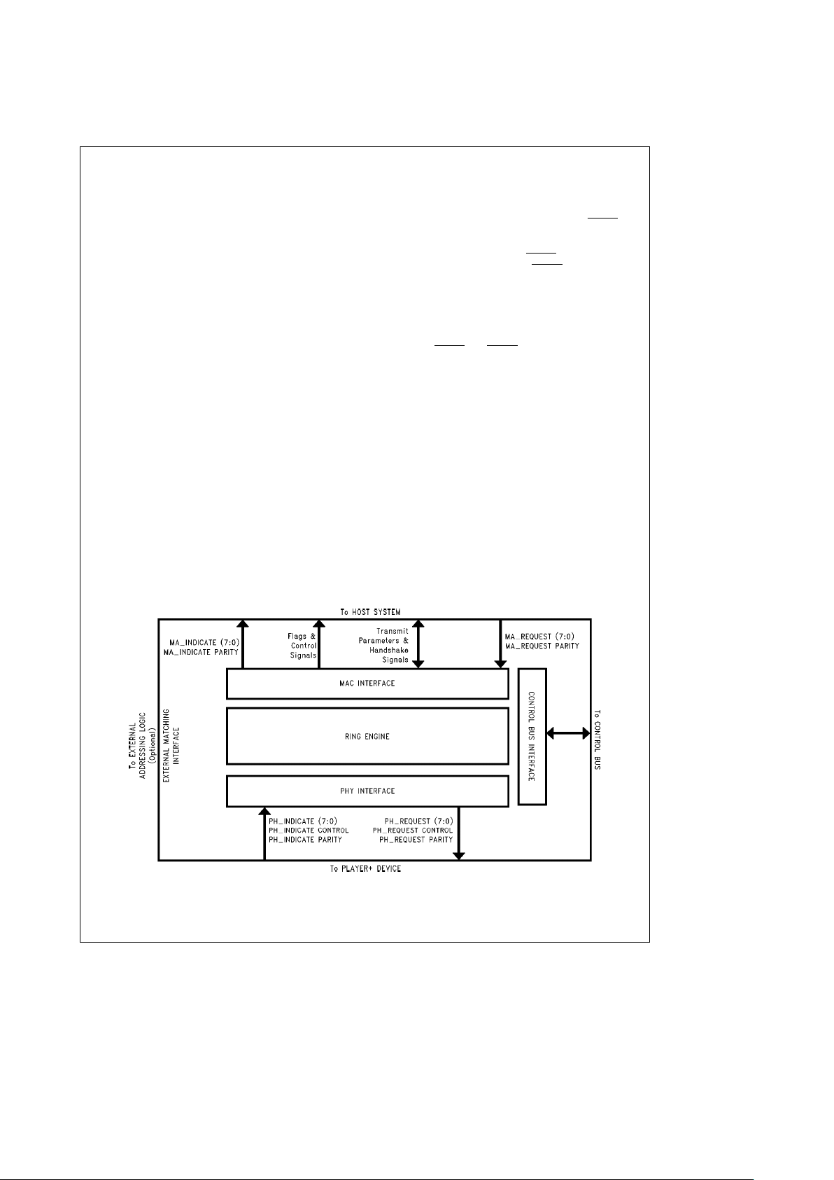
3.0 Architectural Description
The MACSI is derived from the BMAC and BSI devices. The
MACSI is composed of the Ring Engine, the Service Engine,
and the Bus Interface Unit. The Ring Engine performs the
FDDI MAC Timed token protocol and contains the MAC
transmitter and receiver. The Service Engine implements
the Request and Indicate Data Services and contains the
Transmit and Receive Data FIFOs. The Bus Interface Unit
implements the high speed synchronous bus handshake
and contains the Burst FIFOs.
The MACSI device uses a full duplex architecture and provides sufficient bandwidth at the ABus for full duplex transmission with support for through parity.
Figure 3-1
shows
the MACSI device architecture.
TL/F/11705– 2
FIGURE 3-1. MACSI Device Block Diagram
6
3.0 Architectural Description (Continued)
3.1 INTERFACES
3.1.1 PHY Interface
The PHY Interface is a synchronous interface that provides
a byte stream to the PLAYER
a
device (the PHY Request
byte stream, PHYÐRequest), and receives a byte stream
from the PLAYER
a
device (the PHY Indicate byte stream,
PHYÐIndicate).
The 10 bits transferred in both directions across the
PHÐIndicate and PHÐRequest Interfaces consists of one
parity bit (odd parity), one control bit, and 8 bits of data. The
control bit determines if the 8 data bits are a data symbol
pair or a control symbol pair.
3.1.2 ABus Interface
The ABus interface provides the high performance synchronous Data and Control interface to the Host System and/or
local memory. Data and Descriptors are transferred via this
interface over the 32-bit Data bus (with byte parity). Both
multiplexed and non-multiplexed address information is
available on this bus. Arbitration and transfer control signals
are provided and minimize the requirements for external
glue logic.
3.1.3 Control Bus Interface
The Control Interface implements the interface to the Control Bus which allows the user to initialize, monitor and diagnose the operation of the MACSI. The Control Interface is
an 8-bit interface. This reduces the pinout and minimizes
board space. All information that must be synchronized with
the data stream crosses the ABus Interface.
The Control Bus is separated completely from the high performance data path in order to allow independent operation
of the processor on the Control Bus. The Control Interface
provides synchronization between the asynchronous Control Bus and the synchronous operation of the device.
During operation, the host uses the Control Bus to access
the device’s internal registers, and to manage the attention/
notify (interrupt) logic.
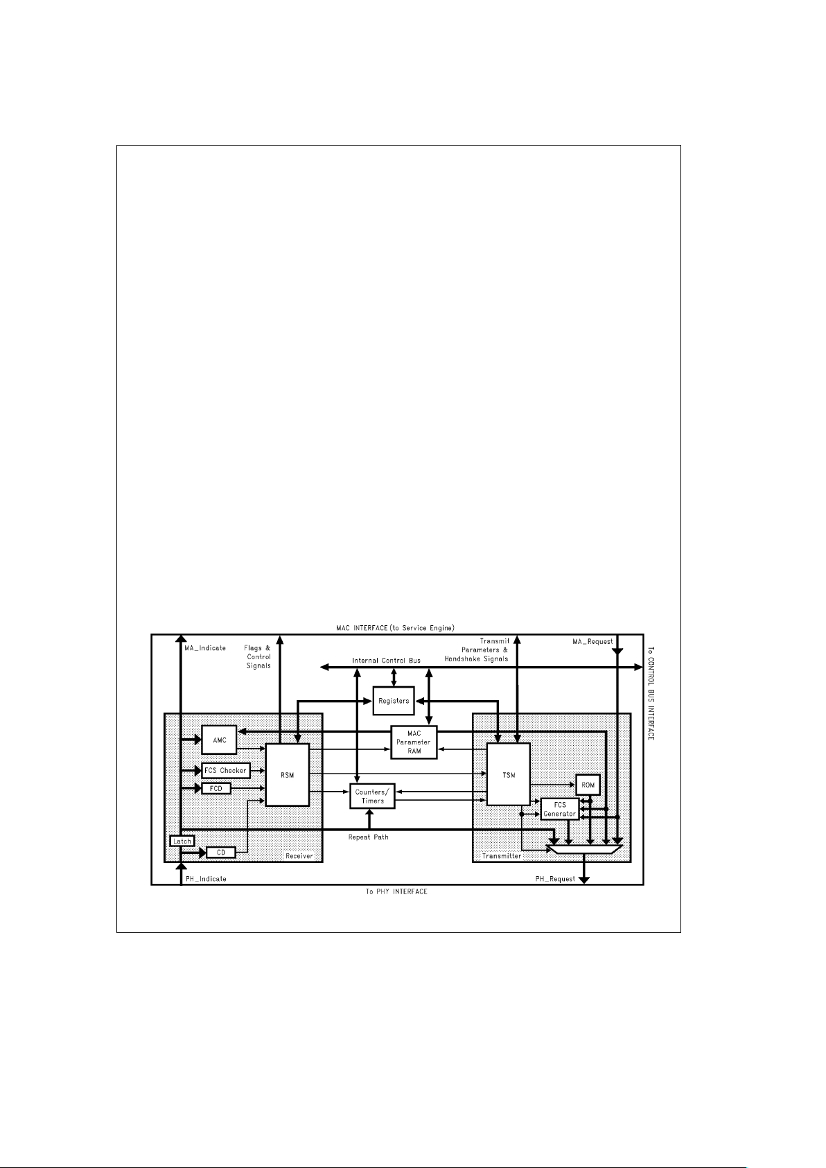
3.2 RING ENGINE
The Ring Engine consists of four blocks: Receiver, Transmitter, MAC Parameter RAM, and Counters/Timers as
shown in
Figure 3-2.
3.2.1 Receiver
The Receiver accepts data from the PHY level device in
byte stream format (PHÐIndicate).
Upon receiving the data, the Receiver performs the following functions:
#
Determines the beginning and ending of a Protocol Data
Unit (PDU)
#
Decodes the Frame Control field to determine the PDU
type (frame or token)
#
Compares the received Destination and Source Addresses with the internal addresses
#
Processes data within the frame
#
Calculates and checks the Frame Check Sequence at
the end of the frame
#
Checks the Frame Status field
And finally, the Receiver presents the data to the MAC Interface along with the appropriate control signals
(MAÐIndicate).
3.2.2 Transmitter
The Transmitter inserts frames from this station into the ring
in accordance with the FDDI Timed-Token MAC protocol. It
also repeats frames from other stations in the ring. The
Transmitter block multiplexes data from the MAÐRequest
Interface and data from the Receiver Block. During frame
transmission, data from the Request Interface is selected.
During frame repeating, data from the Receiver is selected.
TL/F/11705– 3
FIGURE 3-2. Ring Engine Block Diagram
7

3.0 Architectural Description (Continued)
During frame transmission, the Transmitter performs the following functions:
#
Captures a token to gain the right to transmit
#
Transmits one or more frames
#
Generates the Frame Check Sequence and appends it at
the end of the frame
#
Generates the Frame Status field that is transmitted at
the end of the frame
#
Issues the token at the end of frame transmission
During frame repeating, the Transmitter performs the following functions:
#
Repeats the received frame and modifies the Frame
Status field at the end of the frame as specified by the
standard
Whether transmitting or repeating frames, the Transmitter
also performs the following functions:
#
Strips the frame(s) that are transmitted by this station
#
Generates Idle symbols between frames
Data is presented from the Transmitter to the PLAYER
a
device in byte stream format (PHÐRequest).
3.2.3 MAC Parameter RAM
The MAC Parameter RAM is a dual port RAM that contains
MAC parameters such as the station’s short and long addresses. These parameters are initialized via the Control
Interface. Both the Receiver and Transmitter Blocks access
the RAM.
The Receiver uses these parameters to compare addresses
in incoming frames with the individual and group addresses
stored in the Parameter RAM.
The Transmitter uses the Parameter RAM for generating the
Source Address for all frames (except when Source Address Transparency is enabled) and for the Destination Address and Information fields on Claim and Beacon frames.
3.2.4 Counters/Timers
The Counter/Timer Block maintains all of the counters and
timers required by the ANSI X3T9.5 MAC standard.
Events which occur too rapidly for software to count, such
as the various Frame Counts, are included in the Event
Counters. The size of the wrap around counters has been
chosen to require minimal software intervention even under
marginal operating conditions. Most of the counters increment in response to events detected by the Receiver. The
counters are readable via the Control Interface.
The Token Rotation and Token Holding Timers which are
used to implement the Timed Token Protocol are contained
within the Timer Block.
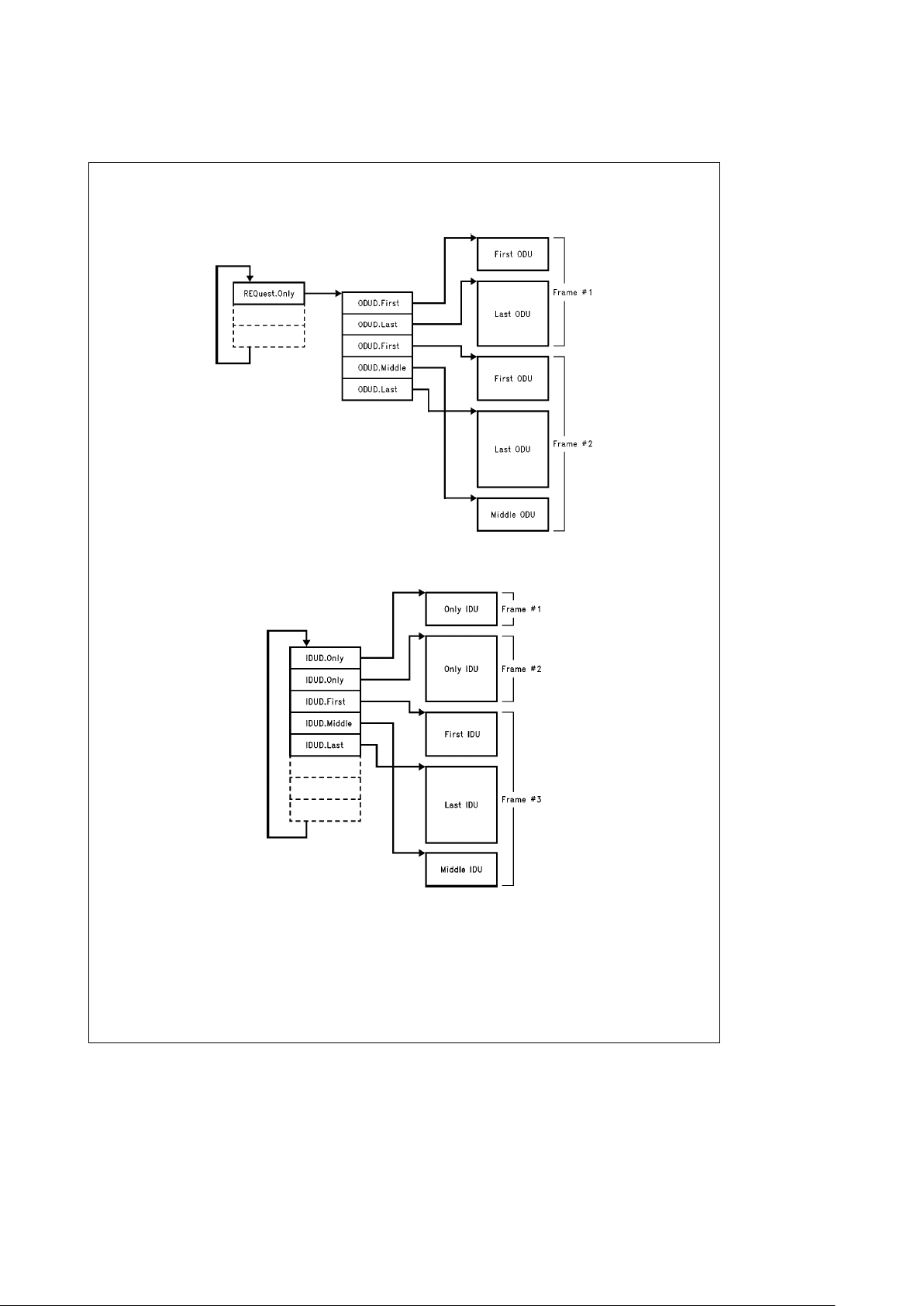
3.3 DATA STRUCTURES
3.3.1 Data Types
The architecture of the MACSI device defines two basic
types of objects: Data Units and Descriptors. A Data Unit is
a group of contiguous bytes which forms all or part of a
frame. A Descriptor is a two-word (64-bit) control object that
provides addressing information and control/status information about MACSI device operations.
Data and Descriptor objects may consist of one or more
parts, where each part is contiguous and wholly contained
within a memory page. Descriptor pages are selectable as
all 1 kBytes or all 4 kBytes. Data Units are described by
Descriptors with a pointer and a count. A single Data Unit
may not cross a 4k boundary. All Descriptors may be
marked as First, Middle, Last, or Only. Thus, multiple Descriptors may be combined to describe a single entity (i.e.
one frame). A single-part object consists of one Only Part; a
multiple-part object consists of one First Part, zero or more
Middle Parts, and one Last Part. In Descriptor names, the
object part is denoted in a suffix, preceded by a dot. Thus
an Input Data Unit Descriptor (IDUD), which describes the
last Data Unit of a frame received from the ring, is called an
IDUD.Last.
A Data Unit is stored in contiguous locations within a single
4 kByte page in memory. Multiple-part Data Units are stored
in separate, and not necessarily contiguous 4 kByte pages.
Descriptors are stored in contiguous locations in Queues
and Lists, where each Queue occupies a single 1 kByte or
4 kByte memory page, aligned on the queue-size boundary.
For Queues, an access to the next location after the end of
a page will automatically wrap-around and access the first
location in the page.
Data Units are transferred between the MACSI’s Service
Engine and Ring Engine via five simplex Channels, three
used for Indicate (receive) data and two for Request (transmit) data. Parts of frames received from the ring and copied
to memory are called Input Data Units (IDUs); parts of
frames read from memory to be transmitted to the ring are
called Output Data Units (ODUs).
Descriptors are transferred between the MACSI device and
Host via the ABus, whose operation is for the most part
transparent to the user. There are five Descriptor types recognized by the MACSI device: Input Data Unit Descriptors
(IDUDs), Output Data Unit Descriptors (ODUDs), Pool
Space Descriptors (PSPs), Request Descriptors (REQs),
and Confirmation Message Descriptors (CNFs).
Input and Output Data Unit Descriptors describe a single
Data Unit part, i.e., its address (page number and offset), its
size in bytes, and its part (Only, First, Middle, or Last).
Frames consisting of a single part are described by a Descriptor.Only; frames consisting of multiple parts are described by a single Descriptor.First, zero or more Descriptor.Middles, and a single Descriptor.Last.
Every Output Data Unit part is described by an ODUD. Output Data Unit Descriptors are fetched from memory so that
frame parts can be assembled for transmission.
Every Input Data Unit part is described by an Input Data Unit
Descriptor (IDUD). Input Data Unit Descriptors are generated on Indicate Channels to describe where the MACSI device wrote each frame part and to report status for the
frame.
Request Descriptors (REQs) are written by the user to specify the operational parameters for the MACSI device Request operations. Request Descriptors also contain the start
address of part of a stream of ODUDs and the number of
frames represented by the ODUD stream part (i.e., the number of ODUD.Last descriptors). Typically, the user will define
a single Request Object consisting of multiple frames of the
same request and service class, frame control, and expected status.
8

3.0 Architectural Description (Continued)
Confirmation Messages (CNFs) are created by the MACSI
device to record the result of a Request operation.
Pool Space Descriptors (PSPs) describe the location and
size of a region of memory space available for writing Input
Data Units.
Request (transmit) and Indicate (receive) data structures
are summarized in
Figure 3-3.
3.3.2 Descriptor Queues and Lists
The MACSI device uses 10 Queues and two Lists which are
circular. There are six Queues for Indicate operations, and
four Queues and two Lists for Request operations. Each of
the three Indicate Channels has a Data Queue containing
Pool Space Descriptors (PSPs), and a Status Queue containing Input Data Unit Descriptors (IDUDs). Each Request
Channel has a Data Queue containing Request Descriptors
(REQs), a Status Queue containing Confirmation Messages
(CNFs), and a List containing Output Data Unit Descriptors
(ODUDs).
During Indicate and Request operations, Descriptor Queues
and Lists are read and written by the MACSI device, using
registers in the Pointer and Limit RAM Register files. The
Pointer RAM Queue and List Pointer Registers point to a
location from which a Descriptor will be read (PSPs and
REQs) or written (IDUDs and CNFs). All of the Queues and
Lists are strictly unidirectional. The MACSI consumes objects in those queues which are produced by the Host. The
Host consumes objects in those queues which are produced by the MACSI.
For each Queue Pointer Register there is a corresponding
Queue Limit Register in the Limit RAM Register file, which
holds the Queue’s limit as an offset value in units of 1 Descriptor (8 bytes). The address in the Queue Pointer is incremented before a Descriptor is read and after a Descriptor is
written, then compared with the value in the corresponding
Queue Limit Register. When a Queue Pointer Register becomes equal to the Queue Limit Register, an attention is
generated, informing the host that the Queue is empty.
When a pointer value is incremented past the end of the
page, it wraps to the beginning of the page.
3.3.3 Storage Allocation
The maximum unit of contiguous storage allocation in external memory is a Page. All MACSI device addresses consist
of a 16-bit page number and a 12-bit offset.
The MACSI device uses a page size of 1 kByte or 4 kBytes
for storage of Descriptor Queues and Lists (as selected by
the user), and a page size of 4 kBytes for storage of Data
Units. A single page may contain multiple Data Units, and
multiple-part Data Units may span multiple, disjoint or contiguous pages.
3.4 SERVICE ENGINE
The Service Engine, which manages the operation of the
MACSI, contains seven basic blocks: Indicate Machine, Request Machine, Status/Space State Machine, Pointer RAM,
Limit RAM, and Bus Interface Unit. An internal block diagram of the Service Engine is shown in
Figure 3-4.
3.4.1 Indicate Machine
The Indicate Block accepts Service Data Units (frames)
from the Ring Engine (MAC) in a byte stream format
(MAÐIndicate).
9
3.0 Architectural Description (Continued)
Request Data Structures
TL/F/11705– 4
Indicate Data Structures
TL/F/11705– 5
FIGURE 3-3. MACSI Device Data Structures
10
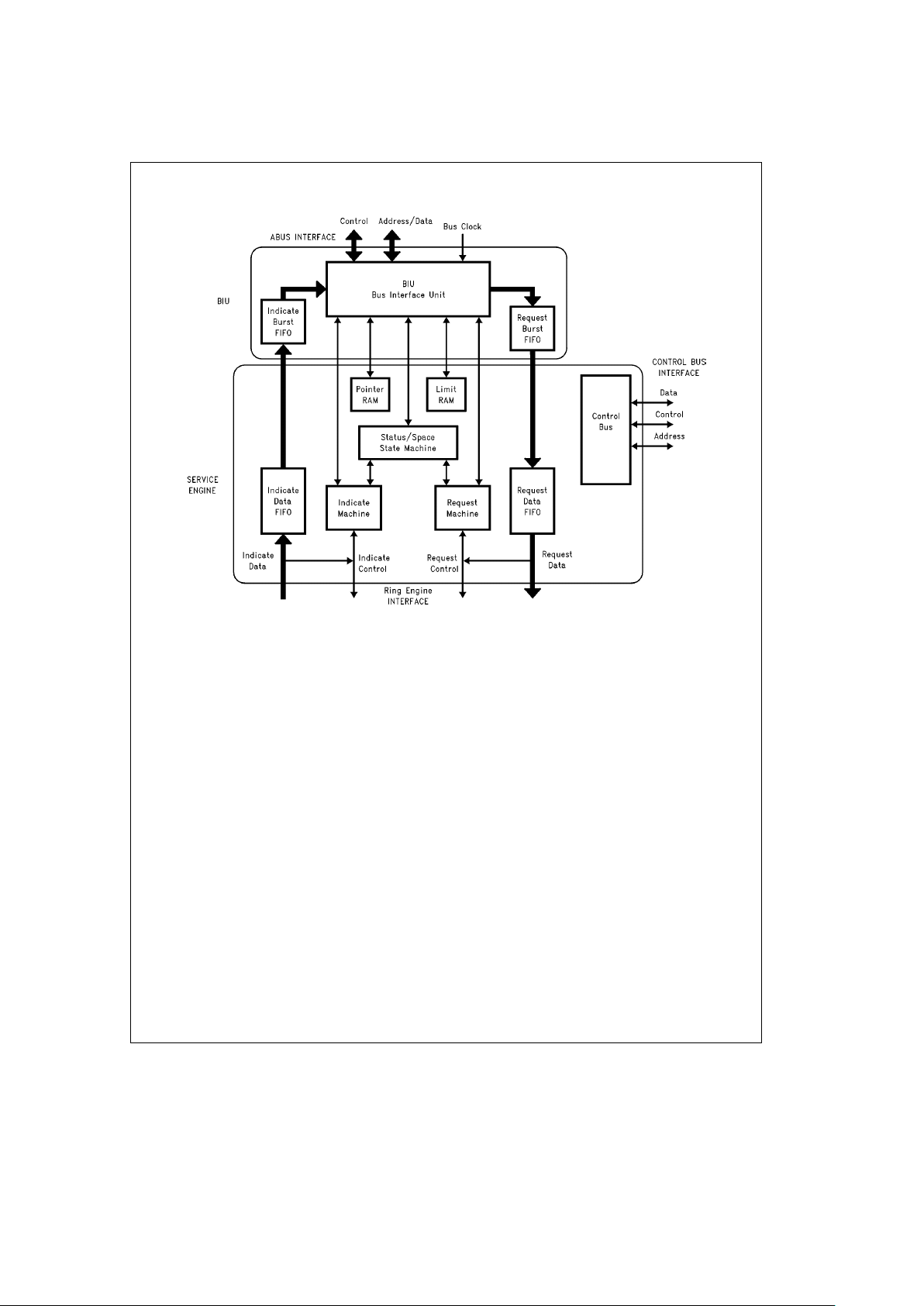
3.0 Architectural Description (Continued)
TL/F/11705– 6
FIGURE 3-4. Service Engine/BIU Internal Block Diagram
Upon receiving the data, the Indicate Block performs the
following functions:
#
Decodes the Frame Control field to determine frame type
#
Sorts received frames onto Channels according to the
Sort Mode
#
Optionally Filters identical MAC frames
#
Filters Void frames
#
Copies the received frames to memory according to
Copy Criteria
#
Writes status for the received frames to the Indicate
Status Queue
#
Issues interrupts to the host at host-defined status breakpoints
3.4.2 Request Machine
The Request Machine presents frames to the Ring Engine
(MAC) in a byte stream format (MAÐRequest).
The Request Machine performs the following functions:
#
Reads frames from host memory and assembles them
onto Request Channels
#
Prioritizes active requests
#
Transmits frames to the Ring Engine (MAC)
#
Optionally writes status for transmitted and returning
frames
#
Issues interrupts to the host on user-defined group
boundaries
3.4.3 Status/Space Machine
The Status/Space Machine is used by both the Indicate Machine and the Request Machine.
The Status/Space Machine manages all descriptor Queues
and writes status for received and transmitted frames.
3.4.4 Bus Interface Unit
The Bus Interface Unit (BIU) is used by both the Indicate
and Request Blocks. It manages the ABus Interface, providing the MACSI device with a 32-bit data path to local or
system memory.
The Bus Interface Unit controls the transfer of Data Units
and Descriptors between the MACSI device and Host memory via the ABus.
Data and Descriptors are transferred between the MACSI
device and Host memory. Each Channel type handles a set
of Data and Descriptor objects. The three Indicate (Receive)
Channels use the following objects:
1. Input Data Units (written by MACSI)
2. Input Data Unit Descriptors (written by MACSI)
3. Pool Space Descriptors (read by MACSI)
The two Request (Transmit) Channels each use the following objects:
1. Output Data Units (read by MACSI)
2. Output Data Unit Descriptors (read by MACSI)
3. Confirmation Message Descriptors (written by MACSI)
4. Request Descriptors (read by MACSI)
11

3.0 Architectural Description
(Continued)
Each Channel will only process one object type at a time.
The BIU arbitrates between the Channels and issues a Bus
Request when any Channel requests service. The priority of
Channel bus requests is as follows, from highest priority to
lowest priority:
1. Indicate Data Unit writes (highest priority when not transmitting)
2. Output Data Unit fetches (highest priority when transmitting)
3. Request Descriptor and Output Data Unit Descriptor
fetches
4. Input Data Unit Descriptor writes
5. Confirmation Message Descriptor writes
6. Next Pool Space Descriptor transfer to Current Pool
Space Descriptor (internal operation)
7. Pool Space Descriptor fetches
8. Limit RAM Operations (internal operation)
9. Pointer RAM Operations (lowest priority)
Addresses for Channel accesses are contained in the Pointer RAM Registers.
3.4.5 Pointer RAM
The Pointer RAM Block is used by both the Indicate and
Request Machines. It contains pointers to all Data Units and
Descriptors manipulated by the MACSI device, namely, Input and Output Data Units, Input and Output Data Unit Descriptors, Request Descriptors, Confirmation Message Descriptors, and Pool Space Descriptors.
The Pointer RAM Block is accessed by clearing the PTOP
(Pointer RAM Operation) bit in the Service Attention Register, which causes the transfer of data between the Pointer
RAM Register and a mailbox location in memory.
3.4.6 Limit RAM
The Limit RAM Block is used by both the Indicate and Request Machines. It contains data values that define the limits of the ten Queues maintained by the MACSI device.
Limit RAM Registers are accessed by clearing the LMOP
(Limit RAM Operation) bit in the Service Attention Register,
which causes the transfer of data between the Limit RAM
Register and the Limit Data and Limit Address Registers.
4.0 FDDI MAC Facilities
4.1 SYMBOL SET
The Ring Engine (MAC) recognizes and generates a set of
symbols. These symbols are used to convey Line States
(such as the Idle Line State), Control Sequences (such as
the Starting and Ending Delimiters) and Data.
Additional information regarding the symbol set can be
found in the ANSI X3T9.5 PHY standard.
The Ring Engine expects that the Starting Delimiter will always be conveyed on an even symbol pair boundary (i.e.,
the JK symbol will always arrive as a byte, not split across
two bytes). Following the starting delimiter, data symbols
should always come in matched pairs. Similarly the Ending
Delimiter should always come in one or more matched symbol pairs.
The symbol pairs conveyed at the PHY Interface are shown
in Table 4-1.
4.2 PROTOCOL DATA UNITS
The Ring Engine recognizes and generates Tokens and
Frames.
The Token is used to control access to the ring. Only the
station that has captured the token has the right to transmit
new information. The format of a token is shown in
Figure
4-1.
TABLE 4-1. Symbol Pair Set
Type Symbols
Starting Delimiter JK or IL
Ending Delimiter TT or TR or TS or TI
Frame Status RR or RS or SR or SS
Idle II or nI
Data Pair nn
n represents any data symbol (0 –F).
Symbol pairs other than the defined symbols are treated as code violations.
Additional information on the symbol pairs generated and interpreted by the
Ring Engine can be found in Section 8.2.1.
TABLE 4-2. Frame Fields
Name Description Size
SFS Start of Frame
Sequence
PA Preamble 8 or more Idle
symbol pairs
SD Starting Delimiter JK symbol pair
FC Frame Control Field 1 data symbol pair
DA Destination Address 2 or 6 symbol pairs
SA Source Address 2 or 6 symbol pairs
INFO Information Field
FCS Frame Check 4 symbol pairs
Sequence
EFS End of Frame
Sequence
ED Ending Delimiter at least 1 T symbol
for Frames;
at least 2 T symbols
for Tokens
FS Frame Status 3 or more R or S
symbols
SFS EFS
PA SD FC ED
FIGURE 4-1. Token Format
Frames are used to pass information between stations. The
format of a frame is shown in
Figure 4-2,
with the field defini-
tions in Table 4-2.
SFS Protected by FCS EFS
PA SD FC DA SA INFO FCS ED FS
FIGURE 4-2. Frame Format
12

4.0 FDDI MAC Facilities (Continued)
4.2.1 Frame Fields
Start of Frame Sequence (SFS)
The Start of Frame Sequence consists of the Preamble (PA)
followed by the Starting Delimiter (SD).
The Preamble is a sequence of zero or more Idle symbols
that is used to separate frames. The Ring Engine Receiver
can process and repeat a frame or token with no preamble.
The Ring Engine Transmitter generates frames with at least
8 bytes of preamble. The Ring Engine Transmitter also
guarantees that valid FDDl frames will never be transmitted
with more than 40 bytes of preamble.
The Starting Delimiter is used to indicate the start of a new
frame. The Starting Delimiter is the JK Symbol pair.
The Ring Engine expects the Starting Delimiter to be conveyed across the PHÐIndication Interface as a single byte.
Similarly, the Ring Engine only generates Starting Delimiters
aligned to the byte boundary.
Frame Control (FC)
The Frame Control field is used to discriminate frames. For
tokens, the FC field identifies Restricted and Non-restricted
tokens. For other frames, the FC field identifies the frame
type and format and how the frame is to be processed.
The one byte FC field is formatted as shown in
Figure 4-3
.
CLFFrZZZ
FIGURE 4-3. Frame Control Field
The C (Class) bit specifies the MAC Service Class as Asynchronous (C
e
0) or Synchronous (Ce1).
The L (Length) bit specifies the length of the MAC Address
as Short (L
e
0) or Long (Le1). A Short Address is a
16-bit address. A Long Address is a 48-bit address.
The FF (Format) bits specify the frame types as shown in
Table 4-3.
The r (Reserved) bit is currently not specified and should
always be transmitted as Zero.
The ZZZ (Control) bits are used in conjunction with the C
and FF bits to specify the type of frames. These bits may be
used to affect protocol processing criteria such as the Priority, Protocol Class, Status Handling, etc.
TABLE 4-3. Frame Control Format Bits
FC.FF Frame Types
0 0 SMT/MAC
0 1 LLC
1 0 reserved for implementer
1 1 reserved for future standardization
When the Frame Control Format bits (FC.FF) indicate an
SMT or MAC frame, the frame type is identified as shown in
Table 4-4.
TABLE 4-4. MAC/SMT Frame Types
CLFF rZZZ Frame Type
1000 0000 Non-restricted Token
1100 0000 Restricted Token
0L00 0000 Void Frame
0L00 0001 to 1110 SMT Frame
0L00 1111 SMT Next Station Addressing Frame
1L00 0001 Other MAC Frame
1L00 0010 MAC Beacon Frame
1L00 0011 MAC Claim Frame
1L00 0100 MAC Purge Frame
1L00 0101 to 1111 Other MAC Frame
Destination Address (DA)
The Destination Address (DA) field is used to specify the
station(s) that should receive and process the frame.
The DA can be an Individual or Group address. This is determined by the Most Significant Bit of the DA (DA.lG).
When DA.IG is 0 the DA is an Individual Address, when
DA.lG is 1 the DA is a Group Address. The Broadcast/Universal address is a Group Address.
The DA field can be a Long or Short Address. This is determined by the L bit in the FC field (FC.L). If FC.L is 1, the DA
is a 48-bit Long Address. If FC.L is 0, the DA is a 16-bit
Short Address.
The Ring Engine maintains a 16-bit Individual Address (My
Short Address (MSA)), and a 48-bit Individual Address (My
Long Address (MLA)).
On the receive side, if DA.lG is 0 the incoming DA is compared with MLA (if FC.L
e
1) or MSA (if FC.Le0). If the
received DA matches MLA or MSA the frame is intended for
this station and the address recognized flag (AÐFlag) is set.
If DA.lG is 1, the DA is a Group Address and is compared
with the set of Group Addresses recognized by the Ring
Engine. If a match occurs the address recognized flag
(AÐFlag) is set. The AÐFlag is used by system interface
logic as part of the criteria (with FC.L, DA.lG and MÐFlag)
to determine whether or not to copy the frame. lf the
AÐFlag is set, the system interface will normally attempt to
copy the frame.
On the transmit side, the DA is provided by the system interface logic as part of the data stream. The length of the
address to be transmitted is determined by the L bit of the
FC field. (The FC field is also passed in the data stream.)
The Destination Address can be an Individual, Group, or
Broadcast Address.
Source Address (SA)
The Source Address (SA) field is used to specify the address of the station that originally transmitted the frame.
The Source Address has the same length as the Destination
Address (i.e., if the DA is a 16-bit Address, the SA is a 16-bit
Address; if the DA is a 48-bit Address, the SA is a 48-bit
Address).
13

4.0 FDDI MAC Facilities (Continued)
On the receive side, the incoming SA is compared with either MSA or MLA. If a match occurs between the incoming
SA and this station’s MLA or MSA, the MFlag is set. This
flag is used to indicate that the frame is recognized as having been transmitted by this station and is stripped. The
most significant bit of the SA (SA.lG) is not evaluated in the
comparison.
On the transmit side, the station’s individual address is
transmitted as the SA. Since the SA field is normally used
for stripping frames from the ring, the SA stored by the Ring
Engine normally replaces the SA from the data stream. The
length of the address to be transmitted is determined by the
L bit of the FC field. (The FC field is passed in the data
stream.) The most significant bit of the SA (SA.IG) is normally transmitted as 0, independent of the value passed
through the data stream.
As a transmission option, the SA may also be transmitted
transparently from the data stream. When the SA Transparency option is used, an alternate stripping mechanism is
necessary to remove these frames from the ring. (The Ring
Engine provides a Void Stripping Option; see Request
Channel 0 and 1 Configuration Registers 0 (R0CR0 and
R1CR0) for further information.)
As a separate and independent transmission option, the
MSB of the SA may also be transmitted transparently from
the data stream. This is useful for end stations participating
in the Source Routing protocol that would like to continue to
perform reliable stripping based on the SA. (When this option is used without SAT, the transmitted SA is generated by
the Ring Engine, as always.)
Information (INFO)
The Information field contains the data transferred between
peer users of the MAC data service (SMT, LLC, etc.). There
is no INFO field in a Token.
The INFO field contains zero or more bytes.
On the receive side, the INFO field is checked to ensure
that it has at least the minimum length for the frame type
and contains an even number of symbols, as required by the
ANSl X3T9.5 MAC standard.
The first 4 bytes of the INFO field of MAC frames are stored
in an internal register and compared against the INFO field
of the next MAC frame. If the data of the two frames match
and both frames were MAC frames, the SameInfo signal is
generated. This signal may be used to copy MAC frames
only when new information is present.
On the transmit side, the Ring Engine does not limit the
maximum size of the INFO field, but it does insure that
frames are transmitted with a valid DA and SA.
Frame Check Sequence (FCS)
The Frame Check Sequence is a 32-bit Cyclic Redundancy
Check that is used to check for data corruption in frames.
There is no FCS field in a Token.
On the receive side, the Ring Engine checks the FCS to
determine whether the frame is valid or corrupted.
On the transmit side, the FCS field is appended to the end
of the INFO field. As a transmission option, appending the
FCS to the frame can be inhibited (FCS Transparency).
End of Frame Sequence (EFS)
The End of Frame Sequence (EFS) always begins with a T
symbol and should always contain an even number of symbols. For Tokens, an additional T symbol is added. For
frames, the Ending Delimiter (ED) is followed by one or
more of Frame Status Indicators (FS).
The Frame Status (FS) field is used to indicate the status of
the frame. The FS field consists of three Indicators: Error
Detected (E), Address Recognized (A), and Frame Copied
(C). These Indicators are created and modified as specified
in the ANSl X3T9.5 MAC standard.
For frames transmitted by the Ring Engine, the E, A and C
Indicators are appended to all frames and are transmitted
as R symbols. No provisions are made to generate additional trailing control indicators.
For frames repeated by the Ring Engine, the E, A and C
Indicators are handled as specified in the Standard. Additional trailing control indicators are repeated unmodified
provided they are properly aligned. See Section 5.5 for details on Frame Status Processing.
4.2.2 Token Formats
The Ring Engine supports non-restricted and restricted Tokens. See
Figure 4-4
and
Figure 4-5
.
SFS FC EFS
SD 80 ED
FIGURE 4-4. Non-Restricted Token Format
SFS FC ED
SD C0 ED
FIGURE 4-5. Restricted Token Format
Non-restricted
A non-restricted token is used for synchronous and non-restricted asynchronous transmissions. Each time the non-restricted token arrives, a station is permitted to transmit one
or more frames in accordance with its synchronous bandwidth allocation regardless of the status of the token (late or
early).
Asynchronous transmissions occur only if the token is early
(usable token) and the Token Holding Timer has not
reached the selected threshold.
Restricted
A restricted token is used for synchronous and restricted
asynchronous transmissions only.
A station which initiates the restricted dialogue captures a
non-restricted token and releases a restricted token. Stations that participate in the restricted dialogue are allowed
to capture the restricted token. A station ends the restricted
dialogue by capturing the restricted token and releasing a
non-restricted token.
4.2.3 Frame Formats
The Ring Engine supports all of the frame formats permitted
by the FDDl standard. All frame types may be created extemal to the Ring Engine and be passed through the MAC
Request Interface to the Ring. The Ring Engine also has the
ability to generate Void, Beacon, and Claim frames internally.
14

4.0 FDDI MAC Facilities (Continued)
Frames Generated Externally
The Ring Engine transmits frames passed to it from the System Interface. The data portion of the frame is created by
the System Interface. The data portion begins with the FC
field and ends with the last byte of the INFO field. The FC
field is passed transparently to the ring. The length bit in the
FC field is used to determine the length of the transmitted
addresses. The data is passed as a byte stream across the
MAC Request Interface as shown in Table 4-5.
TABLE 4-5. Frame Formats
Field
Size
MAÐRequest PHÐRequest
(bytes)
PA
t8;s
40 Idle Pairs
SD 1 JK
FC 1 FC FC
DA 2 or 6 DA DA
SA 2 or 6 SA MSA, MLA, or SA
INFO
t
0 INFO INFO
FCS 4 if present FCS FCS
ED 1 TR
FS 1 RR
Before the frame is transmitted, the Ring Engine inserts the
Start of Frame Sequence with at least 8 bytes of Preamble
but no more than 40 bytes of Preamble. The starting delimiter is transmitted as a JK symbol pair. The Source Address
is normally transmitted by the Ring Engine since it uses the
Source Address to determine when to strip a frame from the
ring. This can be overridden by using the Source Address
transparency capability. Similarly, the Frame Check Sequence (4 bytes) is normally transmitted by the Ring Engine.
This can be overridden with the FCS transparency capability. With FCS transparency, the FCS is transmitted from the
data stream. The End of Frame Sequence is always transmitted by the Ring Engine as TR RR.
Frames Generated by Ring Engine
The Ring Engine generates and detects several frames in
order to attain and maintain an operational ring.
Void Frames
Void frames are used during normal operation. The Ring
Engine generates two types of void frames: regular Void
frames and MyÐVoid frames.
If Short addressing is enabled, Void frames with the short
address (MSA) are transmitted. Otherwise, Void frames with
the long address (MLA) are transmitted. Table 4-6 shows
the Void frame format.
Void frames are transmitted in order to reset the Valid
Transmission timers (TVX) in other stations to eliminate unnecessary entry to the Claim state. Stations are not required
to copy Void frames. Void frames are transmitted by the
Ring Engine in two situations:
1. While holding a token when no data is ready to be trans-
mitted.
2. After a frame transmission is aborted.
MyÐVoid frames are transmitted by the Ring Engine in
three situations:
1. After a request to measure the Ring Latency has been
made and the next early token is captured.
2. After this station wins the Claim process and before the
token is issued.
3. After a frame has been transmitted with the STRIP op-
tion and before the token for that service opportunity is
issued.
Void frames are also detected by the Ring Engine. A Void
frame with a Source Address other than MSA or MLA is
considered an OtherÐVoid frame.
Claim Frames
Claim frames are generated continuously with minimum preamble while the Ring Engine is in the Transmit Claim state.
The format of Claim frames generated by the Ring Engine is
shown in Table 4-7. When long addressing is enabled,
frames with the long address (MLA) are transmitted. Otherwise frames with the short address (MSA) are transmitted.
The Ring Engine detects reception of valid Claim frames. A
comparison is performed between the first four bytes of the
received INFO field and the value of TREQ programmed in
the parameter RAM in order to distinguish HigherÐClaim,
LowerÐClaim, DuplicateÐClaim, and MyÐClaim.
Beacon Frames
Beacon frames are transmitted continuously with minimum
preamble when the Ring Engine is in the Transmit Beacon
state. The format of Beacon frames generated by the Ring
Engine is shown in Table 4-8. When long addressing is enabled, frames with the long address (MLA) are transmitted.
Otherwise frames with the short address (MSA) are transmitted.
15

4.0 FDDI MAC Facilities (Continued)
TABLE 4-6. Void Frames
Type Enable Size SFS FC DA SA FCS EFS
Void ESA Short PA SD 00 null MSA FCS TRRR
Void not ESA Long PA SD 40 null MLA FCS TRRR
MyÐVoid ESA Short PA SD 00 MSA MSA FCS TRRR
MyÐVoid not ESA Long PA SD 40 MLA MLA FCS TRRR
TABLE 4-7. Claim Frames
Type Enable Size SFS FC DA SA INFO FCS EFS
MyÐClaim not ELA Short PA SD 83 MSA MSA TREQ FCS TRRR
MyÐClaim ELA Long PA SD C3 MLA MLA TREQ FCS TRRR
TABLE 4-8. Beacon Frames
Type Enable Size SFS FC DA SA INFO FCS EFS
MyÐBeacon not ELA Short PA SD 82 null MSA TBT FCS TRRR
MyÐBeacon ELA Long PA SD C2 null MLA TBT FCS TRRR
When the Transmit Beacon State is entered from the Transmit Claim State the first byte of the 4 byte TBT field is transmitted as Zero.
Beacon frames that require alternative formats such as Directed Beacons must be generated externally.
The Ring Engine detects reception of valid Beacon frames
and distinguishes between Beacon frames transmitted by
this MAC (MyÐBeacon) and Beacon frames transmitted by
other stations (OtherÐBeacon).
4.3 FRAME COUNTS
To aid in fault isolation and to enhance the management
capabilities of a ring, the Ring Engine maintains several
frame counts. The Error and lsolated frame counts increment when a frame is received with one or more errors that
were previously undetected. The Ring Engine then modifies
the Error Control Indicator so that a downstream station will
not increment its count.
The size of the counters has been chosen such that minimal
software intervention is required, even under marginal operating conditions.
The following counts are maintained by the Ring Engine:
FRCT Frame Received
ElCT Error lsolated
LFCT Lost Frame
FCCT Frames Copied with Ax set
FNCT Frames Not Copied with Ax set
FTCT Frames Transmitted
4.3.1 Frame Received Count (FRCT)
The Frame Received Count is described in the FDDl MAC
standard, and is the count of all complete frames received.
This count includes frames stripped by this station.
4.3.2 Error lsolated Count (ElCT)
The Error lsolated Count is described in the FDDl MAC standard, and is the count of error frames detected by this station and no previous station. It increments when:
1. An FCS error is detected and the received Error Indicator
(Er) is not equal to S.
2. A frame of invalid length (i.e., off boundary T) is received
and Er is not equal to S.
3. Er is not R or S.
4.3.3 Lost Frame Count (LFCT)
The Lost Frame Count is described in the FDDl MAC standard, and is the count of all instances where a format error
is detected in a frame or token such that the credibility of
reception is placed in doubt. The Lost Frame Count is incremented when any symbol other than data or Idle symbols is
received between the Starting and Ending Delimiters of a
frame (this includes parity errors).
4.3.4 Frame Copied Count (FCCT)
The Frame Copied Count is described in the FDDl MAC
standard, and is the count of the number of frames addressed to and copied by this station. The count is incremented when an internal or external match occurs (when
Option.EMlND enabled) on the Destination Address, no errors were detected in the frame and the frame was successfully copied (which the Service Engine communicates to the
Ring Engine via the internal VCOPY signal). Frames copied
promiscuously, MAC frames, Void frames and NSA frames
received with the A indicator set are not included in this
count.
16

4.0 FDDI MAC Facilities (Continued)
4.3.5 Frames Not Copied Count (FNCT)
The Frames Not Copied Count is specified in the FDDI MAC
standard, and is the count of frames intended for this station
that were not successfully copied by this station. The count
is incremented when an internal or external (when
Option.EMIND is enabled) Destination Address match occurs, no errors were detected in the frame, and the frame
was not successfully copied (VCOPY
e
0). MAC frames,
Void frames, and NSA frames received with the A indicator
set are not included in this count.
4.3.6 Frames Transmitted Count (FTCT)
The Frames Transmitted Count is specified in the FDDI
MAC standard, and is incremented every time a complete
frame is transmitted from the MAC Request Interface. Void
and MAC frames generated by the Ring Engine are not included in the count.
4.4 TIMERS
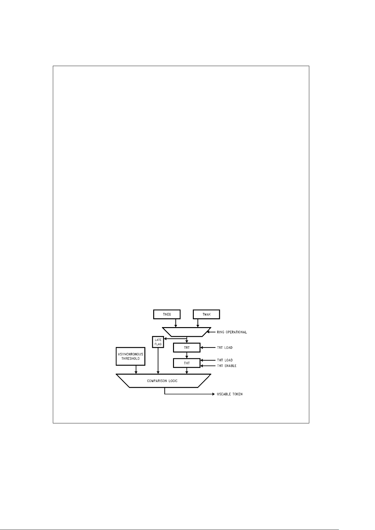
4.4.1 Token Rotation Timer (TRT)
The Token Rotation Timer (TRT) times token rotations from
arrival to arrival. TRT is used to control ring scheduling during normal operation and to detect and recover from serious
ring error situations.
TRT is loaded with the maximum token rotation time, TMAX,
when the ring is not operational. TRT is loaded with the
negotiated Target Token Rotation Time, TNEG, when the
ring is operational.
4.4.2 Token Holding Timer (THT)
The Token Holding Timer is used to limit the amount of ring
bandwidth used by a station for asynchronous traffic once
the token is captured. THT is used to determine if the captured token is (still) usable for asynchronous transmission. A
token is usable for asynchronous traffic if THT has not
reached the selected threshold. Two asynchronous thresholds are supported; one that is fixed at the Negotiated Target Token Rotation Time (TNEG), and one that is programmable at one of 16 Asynchronous Priority Thresholds. Requests to transmit frames at one of the priority thresholds
are serviced when the Token Holding Timer (THT) has not
reached the selected threshold.
4.4.3 Late Count (LTCT)
The Late Count is implemented differently than suggested
by the MAC standard, but provides similar information. The
function of the Late Count is divided between the Late
Ð
Flag that is equivalent to the MAC standard Late Count with
a non-zero value and a separate counter. LateÐFlag is
maintained by the Ring Engine to indicate if it is possible to
send asynchronous traffic. When the ring is operational,
Late Count indicates the time it took the ring to recover the
last time the ring became non-operational. When the ring is
non-operational, Late Count indicates the time it has taken
(so far) to recover the ring.
The Late Count is incremented every time TRT expires
while the ring is non-operational and LateÐFlag is set (once
every TMAX).
The Late Count is provided to assist Station Management,
SMT, in the isolation of serious ring errors. In many situations the ring will recover very quickly and late count will be
of marginal utility. However, in the case of serious ring er-
rors, it is helpful for SMT to know how long it has been since
the ring became non-operational (with TMAX resolution) in
order to determine if it is necessary to invoke recovery procedures. When the ring becomes non-operational, there is
no way to know how long it will stay non-operational. Therefore, a timer is necessary. If the Late Count were not provided, SMT would be forced to start a timer every time the ring
becomes non-operational even though it may seldom be
used. By using the provided Late Count, an SMT implementation may be able to alleviate this additional overhead.
4.4.4 Valid Transmission Timer (TVX)
The Valid Transmission Timer (TVX) is reset every time a
valid frame or token is received. TVX is used to increase the
responsiveness of the ring to errors. Expiration of the TVX
indicates that no frame or token has been received within
the timeout period and causes the Transmitter to invoke the
recovery (Claim) process.
The Value of TVX is also used as the Duplicate MAC frame
detection delay, DMÐMIN. This is the time after which a
MAC frame will be suspected as being generated by another station with this station’s address when the ring is nonoperational.
4.4.5 Token Received Count (TKCT)
The Token Received Count is incremented every time a valid token arrives. The Token Count can be used with the
Ring Latency Count to calculate the average network load
over a period of time. The frequency of token arrival is inversely related to the network load.
4.4.6 Ring Latency Count (RLCT)
The Ring Latency Count is a measurement of time for
frames to propagate around the ring. This counter contains
the last measured ring latency whenever the Ring Latency
Valid bit of the Token Event Register (TELR0.RLVLD) is
One.
The Latency Counter increments every 16 byte times
(1.28 ms) and is used to measure ring latencies up to
1.3421772 seconds directly with accuracy of 1.2 ms. No
overflow or increment event is provided with this counter.
4.5 RING SCHEDULING
FDDI uses a timed token protocol to schedule use of the
ring. The protocol measures load on the network by timing
the rotation of the token. The longer the token rotation time
the greater the instantaneous load on the network. By limiting the transmission of data when the token rotation time
exceeds a target rotation time, a maximum average token
rotation time is realized. The protocol is used to provide
different classes of service.
Multiple classes of service can be accommodated by setting
different target token rotation times for each class of service.
The Ring Engine supports Synchronous, Non-restricted
Asynchronous, Restricted Asynchronous, and Immediate
service classes. The Immediate service class is supported
when the ring is non-operational; the other classes are supported when the ring is operational.
4.5.1 Synchronous Service Class
The Synchronous Service Class may be used to guarantee
a maximum response time (2 times TTRT), minimum bandwidth, or both.
17

4.0 FDDI MAC Facilities (Continued)
Each time the token arrives, a station is permitted to transmit one or more frames in accordance with its synchronous
bandwidth allocation regardless of the status of the token
(late or early; Restricted or Non-Restricted).
Since the Ring Engine does not provide a mechanism for
monitoring a station’s synchronous bandwidth utilization,
the user must insure that no synchronous request requires
more than the allocated bandwidth.
To help ensure that synchronous bandwidth is properly allocated after ring configuration, synchronous requests are not
serviced after a Beacon frame is received. After a major
reconfiguration has occurred, management software must
intervene to verify or modify the current synchronous bandwidth allocation.
4.5.2 Non-Restricted Asynchronous Service Class
The Non-Restricted Asynchronous service class is typically
used with interactive and background traffic. Non-Restricted
Asynchronous requests are serviced only if the token is early and the Token Holding Timer has not reached the selected threshold.
Asynchronous service is available at two priority thresholds,
the Negotiated Target Token Rotation Time plus one programmable threshold. Management software may use the
priority thresholds to discriminate additional classes of traffic based on current loading characteristics of the ring. The
priority thresholds may be determined using the current
TTRT and the Ring Latency. In this case, application software is only concerned with the priority level of a request.
As an option, Asynchronous Requests may be serviced with
THT disabled. This is useful when it is necessary to guarantee that a multi-frame request will be serviced on a single
token opportunity. Because of the possibility of causing late
tokens, this capability should be used with caution, and
should only be allowed when absolutely necessary.
4.5.3 Restricted Asynchronous Service Class
The Restricted Asynchronous service class is useful for
large transfers requiring all of the available Asynchronous
bandwidth. The Restricted Token service is useful for large
transfers requiring all of the available (remaining) asynchronous bandwidth.
The Restricted Token service may also be used for operations requiring instantaneous allocation of the remaining
synchronous bandwidth when Restricted Requests are
serviced with THT disabled. This is useful when it is necessary to guarantee atomicity, i.e., that a multi-frame request
will be serviced on a single token opportunity.
A Restricted dialogue consists of three phases:
1. Initiation of a Restricted dialogue:
#
Capture a Non-restricted Token
#
Transmit zero or more frames to establish a Restricted
dialogue with other stations
#
Issue a Restricted Token to allow other stations in the
dialogue to transmit frames
2. Continuation of a Restricted dialogue:
#
Capture a Restricted Token
#
Transmit zero or more frames to continue the Restricted dialogue
#
Issue a Restricted Token to allow other stations in the
dialogue to transmit frames
3. Termination of a Restricted dialogue:
#
Capture a Restricted Token
#
Transmit zero or more frames to continue the Restricted dialogue
#
Issue a Non-Restricted Token to return to the Non-Restricted service class
Initiation of a Restricted dialogue will prevent all Non-Restricted Asynchronous traffic throughout the ring for the duration of the dialogue, but will not affect Synchronous traffic.
To ensure that the Restricted traffic is operating properly, it
is possible to monitor the use of Restricted Tokens on the
ring. When a Restricted Token is received, the event is
latched and, under program control, may generate an interrupt. In addition, a request to begin a Restricted dialogue
will only be honored if both the previous transmitted Token
and the current received Token were Non-Restricted tokens. This is to ensure that the upper bound on the presence of a Restricted dialogue in the ring is limited to a single
dialogue.
As suggested by the MAC-2 standard, to help ensure that
only one Restricted dialogue will be in progress at any given
time, Restricted Requests are not serviced after a MAC
frame is received until Restricted Requests are explicitly enabled by management software. Since the Claim process
results in the generation of a Non-restricted Token, this prevents stations from initiating another restricted dialogue
without the intervention of management software.
4.5.4 Immediate Service Class
The Immediate Service Class facilitates several non-standard applications and is useful in ring failure recovery (e.g.,
Transmission of Directed Beacons). Certain ring failures
may cause the ring to be unusable for normal traffic, until
the failure is remedied.
Immediate requests are only serviced when the ring is nonoperational. Immediate requests may be serviced from the
Transmitter Data, Claim, and Beacon States. Options are
available to force the Ring Engine to enter the Claim or
Beacon State, to prohibit it from entering the Claim State, or
to remain in the Claim State when receiving MyÐClaim.
On the completion of an Immediate request, a Token (Nonrestricted or Restricted) may optionally be issued. Immediate requests may also be used in non-standard applications
such as a full duplex point to point link.
5.0 Functional Description
(Ring Engine)
5.1 TOKEN HANDLING
5.1.1 Token Timing Logic
The FDDI Ring operates based on the Timed Token Rotation protocol where all stations on the ring negotiate for the
maximum time that the stations have to wait before being
able to transmit frames. This value is termed the Negotiated
Target Token Rotation Time (TTRT). The TTRT value is
stored in the TNEG Register.
Stations negotiate for TTRT based on their TREQ that is
assigned to them upon initialization.
Each station keeps track of the token arrival by setting the
Token Rotation Timer (TRT) to the TTRT value. If the token
18
5.0 Functional Description (Continued)
is not received within TTRT (the token is late), the event is
recorded by setting the LateÐFlag. If the token is not received within twice TTRT (TRT expires and LateÐFlag is
set), there is a potential problem in the ring and the recovery
process is invoked.
Furthermore, the Token Holding Timer (THT) is used to limit
the amount of ring bandwidth used by a station for asynchronous traffic once the token is captured. Asynchronous
traffic is prioritized based on the LateÐFlag which denotes
a threshold at TTRT and an additional Asynchronous Priority Threshold (THSH). The Asynchronous Threshold comparison (Apri 1) is pipelined, so a threshold crossing may not
be detected immediately; however, the possible error is a
fraction of the precision of the threshold values.
The Token Timing Logic consists of two Timers, TRT and
THT, in addition to the TMAX and TNEG values loaded into
these counters (see
Figure 5-1
).
The Timers are implemented as count-up counters that can
increment every 80 ns. The Timers are reset by loading
TNEG or TMAX into the counters where TNEG and TMAX
are unsigned two’s complement numbers. This allows a
Carry flag to denote timer expiration.
On an early token arrival (LateÐFlag is not set), TRT is
loaded with TNEG and counts up. On a late token arrival
(LateÐFlag is set), LateÐFlag is cleared and TRT continues to count. When TRT expires and LateÐFlag is not set,
LateÐFlag is set and TRT is loaded with TNEG.
THT follows the value of TRT until a token is captured.
When a token is captured, TRT may be reloaded with TNEG
while THT continues to count from its previous value (THT
does not wrap around). THT increments when enabled. THT
is disabled during synchronous transmission and a special
class of asynchronous transmission. THT is used to determine if the token is usable for asynchronous requests. For
these purposes, the token is considered late one byte before it is actually late (to promote interoperability with less
careful implementations).
If TRT expires while LateÐFlag is set, TRT is loaded with
TMAX and the recovery process (Claim) is invoked (unless
the Inhibit Recovery Required option is set). The Recovery
Required condition becomes true one byte time after TRT
expires (to promote interoperability with less careful implementations). When TRT expires and the ring is not operational, TRT is loaded with TMAX. TRT is also loaded with
TMAX on a MAC Reset.
5.1.2 Token Recovery
While the ring is operational, every station in the ring uses
the Negotiated Target Token Rotation Time, TNEG. The
MAC implements the protocol for negotiation of this target
token rotation time (TTRT) through the Claim process. The
shortest requested token rotation time is used by all of the
stations in the ring as the TNEG.
If TRT expires with LateÐFlag set, a token has not been
received within twice TTRT (Target Token Rotation Time). If
TVX (Valid Transmission Timer) expires, the station has not
received a valid token within TVX Max. Both these events
require token recovery and cause the Ring Engine to enter
the Claim process.
In the Claim process, a MAC continuously transmits Claim
frames containing TREQ. Should the MAC receive a Claim
frame with a shorter TREQ (larger valueÐHigherÐClaim) it
leaves the Claim State. A station that receives its own Claim
frame gains the right to send the first token and make the
ring operational again. If the Claim Process does not complete successfully, TRT will expire and the Beacon Process
is invoked.
The Beacon Process is used for fault isolation. A station
may invoke the Beacon Process through an
SMÐControl.request(Beacon). When a station enters the
Beacon Process, it continuously sends out Beacon Frames.
The Beacon Process is complete when a station receives its
own Beacon Frame. That station then enters the Claim process, to re-initialize the ring.
5.2 SERVICING TRANSMISSION REQUESTS
A Request to transmit one or more frames is serviced by the
Ring Engine. After a Request is submitted to the Ring Engine, the Ring Engine awaits an appropriate Service Opportunity in which to service the Request. Frames associated
with the Request are transmitted during the Service Opportunity. The definition of a Service Opportunity is different
depending on the operational state of the ring.
TL/F/11705– 7
FIGURE 5-1. Token Timing Logic
19

5.0 Functional Description (Ring Engine) (Continued)
A Service Opportunity begins when the criteria presented to
the Ring Engine are met. This criteria contains the requested service class (sync, async, async priority, immediate) and
the type of token to capture (restricted, non-restricted, any,
none).
During a service opportunity, the Ring Engine guarantees
that a valid frame is sent with at most 40 bytes of preamble
(unless Option.IRPT is set). When data is not ready to be
transmitted, Void frames are transmitted to reset the TVX
timers in all stations. During an immediate request from the
Claim or Beacon state, if the data for external Claim or Beacon frame is not ready to be transmitted, the Ring Engine
will transmit Claim or Beacon frames using the same internal data used for normal Claim and Beacon processing.
5.2.1 Service Opportunity while Ring Operational
Beginning of Service Opportunity
Table 5-1 shows the conditions that must be true when a
valid token is received in order to begin a service opportunity when the ring is operational.
In addition to the criteria mentioned above, additional criteria apply to the servicing of Synchronous and Restricted
Requests.
#
Synchronous Requests are not serviced if
RELR.BCNR
e
1 (see Section 4.5.1).
#
Restricted requests are not serviced when
RELR.MACR
e
1. (see Section 4.5.3).
#
Restricted Dialogues may only begin when a non-restricted token has been received and transmitted (see Section
4.5.3).
End of Service Opportunity
The Service Opportunity continues until either a token is
issued or the ring becomes non-operational.
A token is issued after the current frame, if any, is transmitted when:
1. It is no longer necessary to hold the token
#
All frames of all active requests have been transmitted
2. The token became unusable while servicing a request
#
Asynchronous Priority threshold reached (if an Async
Priority Request is being serviced)
#
THT expired (if enabled)
When the ring becomes non-operational the current frame
transmission is aborted. The ring may go non-operational
while holding a token as a result of any one of the following
conditions being present:
#
A MAC Reset
#
Reception of a valid MAC frame
#
TRT expiration (TRT was reset when the token was captured)
Issue Token Type
The criteria presented to the Ring Engine to begin a service
opportunity also contains the Issue Token Class. The Issue
Token Class is used if servicing of that request was completed (the last frame of that request was transmitted). Otherwise, a token of the capture token class is issued.
TABLE 5-1. Beginning of Service Opportunity
Requested
Requested
Received
Service
Token
Criteria Token
Class
Capture
Class
Class
Asynchronous non-restricted THTlTHSH non-restricted
Priority LateÐFlag
e
0
RingÐOp
e
1
Asynchronous non-restricted LateÐFlage0 non-restricted
RingÐOp
e
1
Asynchronous restricted LateÐFlage0 restricted
RingÐOp
e
1
Synchronous any RingÐOpe1 any
When servicing multiple requests on a single service opportunity, the issue token class of the previous class becomes
the capture class for the next request for purposes of determining usability.
The type of token issued depends on the service class and
the type of token captured as shown in Table 5-2.
5.2.2 Service Opportunity While Ring Not Operational
While the ring is not operational, a service opportunity occurs if an immediate transmission is requested from the
transmitter Data, Claim or Beacon state, and the transmitter
is in the appropriate state.
The service opportunity continues until any one of the following conditions exist:
1. No (additional) frames are to be sent
2. Time TMAX elapses on this request
3. The transmitter exits the requested state
4. The ring becomes operational while servicing an immediate request
5.2.3 Frame Transmission
Frames associated with the current request may be transmitted at any time during a Service Opportunity. In many
applications, data is ready to be transmitted when the Request is presented to the interface. Soon after the Service
Opportunity begins, frame transmission begins. In other applications, in order to minimize the effects of ring latency, it
is desirable to capture the token when no data is ready to
be transmitted. This capability results in wasted ring bandwidth and should be used judiciously.
During transmission, a byte stream is passed from the System Interface to the MAC Request Interface. The data is
passed through the Ring Engine and appears at the PHY
Request Interface two byte times later.
While a frame is being transmitted, the Request parameters
for the next Request (if different) may be presented to the
interface. At the end of the current frame transmission, a
decision is made to continue or cancel the current service
opportunity based on the new Request parameters.
Several errors can occur during a transmission. A transmission may be terminated unsuccessfully because of external
buffering or interface parity errors, internal Ring Engine errors, a MAC reset, or reception of a MAC frame. When a
20

5.0 Functional Description (Ring Engine) (Continued)
transmission is aborted due to an external error (and
Option.IRPT is not set), a Void frame is transmitted to reset
the TVX timers in all stations in the ring. When a frame is
aborted due to a transmission error, the service opportunity
is not automatically ended.
5.3 REQUEST SERVICE PARAMETERS
5.3.1 Request Service Class
The Requested Service corresponds to the Request Service Class and the Token Class parameters of the
(SMÐ)MAÐDATA.request and (SMÐ)MAÐToken.request
primitives as specified in the Standard.
TABLE 5-2. Token Transmission Type
Service Class
Token Token
Captured Issued
Non-restricted Non-restricted Non-restricted
Begin Restricted Non-restricted Restricted
Continue Restricted Restricted Restricted
End Restricted Restricted Non-restricted
Immediate None None
Immediate Non-restricted None Non-restricted
Immediate Restricted None Restricted
14 useful combinations of the requested Service Class
(Non-Restricted Asynchronous, Restricted Asynchronous,
Synchronous, Immediate), the Token Capture and Issue
Class, and THT Enable are supported by the Ring Engine as
shown in Table 5-3.
Requests are serviced on a Service Opportunity meeting
the requested criteria.
A Token Capture Class of non-rstr indicates that the Transmitter Token Class must be Non-Restricted to begin servicing the request. A Token Capture Class of rstr indicates
that the Transmitter Token Class must be Restricted to begin servicing the Request. A Token Issue Class of non-rstr
means that the Transmitter Token Class will be Non-restricted upon completion of the request. A Token Issue Class of
rstr means that the Transmitter Token Class will be Restricted upon completion of the request.
5.3.2 Request Options
The Request options provide the ability for Source Address
Transparency (SAT) and FCS Transparency (FCST). In both
cases, data from the request stream is transmitted in place
of data from the Ring Engine. The use of Source Address
Transparency has no effect on the sequencing of the interface. When Source Address transparency is not used, the
SA from the internal parameter RAM is substituted for the
SA bytes in the request stream, which must still be present.
Since the FCS is appended to the frame, when FCS transparency is not used, no FCS bytes are present in the request stream.
Source Address Transparency (SAT)
Normally, the SA field in a frame is generated by the Ring
Engine using either the MSA or MLA values programmed in
the parameter RAM. When the SA Transparency option is
selected, the SA from the data stream is transmitted in
place of the MSA or MLA. The SAT option can be invoked
on a Request Object via the Request Configuration parameters of the System Interface.
When the SA Transparency option is selected, it is necessary to rely on an alternate stripping mechanism since stripping based on the returning SA only guarantees that frames
with MSA or MLA will be stripped. Either the Void Stripping
option (described below) may be invoked, or external hardware that forces stripping using the EM (External MÐFlag)
signal is required.
The MSB of the SA is not controlled by this option. It is
normally forced to Zero. It can be controlled using the
Source Address MSB Transparency option described below.
SA Transparency is possible for all frames (including MAC
frames). External support is required to limit the use of SA
Transparency to certain MAC Users. SA Transparency
should not be used with externally generated MAC Frames
in order to maintain accountability, but this is not enforced
by the Ring Engine. When SA Transparency is used with
externally generated Beacon Frames that are transmitted
from the Beacon state, the first 4 bytes of the INFO field are
passed transparently from the data stream instead of being
generated by the Ring Engine.
SA Transparency also overrides the Long and Short Addressing enables. For example, if Long Addressing is not
enabled, it is still possible to transmit frames with Long Addresses. Similarly, if Short Addressing is not enabled, it is
still possible to transmit Frames with Short Addresses. This
may be useful in full duplex point to point applications and
for diagnostic purposes.
Source Address Most Significant Bit Transparency
With the Source Address MSB Transparency option, the
MSB of the SA is sourced from the data stream, as opposed
to being transmitted as Zero. The SA MSB Transparency
option is selected through the Request Channel Configuration Registers in the Service Engine.
Unless the Source Address Transparency option is also selected, the rest of the SA is generated by the Ring Engine.
The MSB of the SA is used to denote the presence of the
Routing Information Field used in Source Routing algorithms (as in the IEEE 802.5 protocol). This option is useful
for stations that use Source Routing. In these applications,
the SA can still be generated by the Ring Engine, even
when routing information is inserted into the data stream.
This allows the normal stripping to be accomplished in end
stations implementing Source Routing (without relying on
external software to not create no-owner frames).
Void Stripping
This option is useful for removing bridged and ownerless
frames and remnants (fragments) from the ring.
In the Void Stripping protocol, two MyÐVoid frames are
transmitted at the end of a service opportunity. Stripping
continues until one of the following conditions occur:
#
One MyÐVoid frame returns (The Second MyÐVoid will
be stripped on the basis of the SA)
#
A Token is received
#
An OtherÐVoid is received
#
A MAC frame other than MyÐClaim is received
#
A MAC Reset occurs
21

5.0 Functional Description (Ring Engine) (Continued)
If any frame of a service opportunity requests this option,
then all frames on that service opportunity will be stripped
using this method. Void Stripping is invoked upon the assertion of the STRIP signal at the beginning of a frame transmission.
Void Stripping is also automatically invoked by this station if
it wins the Claim token process before the initial token is
issued. This removes all fragments and ownerless frames
from the ring when the ring becomes operational.
FCS Transparency
Normally, the Ring Engine generates and transmits the
FCS. When the Frame Check Sequence Transparency op-
tion is selected, the Ring Engine device does not append
the FCS to the end of the Information field. This option is
selected by asserting signal FCST.
The receiving stations treat the last four bytes of the data
stream as the FCS.
This option may be useful for end to end FCS coverage
when crossing FDDI bridges, for diagnostic purposes, or in
Implementer frames.
5.4 FRAME VALIDITY PROCESSING
A valid frame is a frame that meets the minimum length
criteria and contains an integral number of data symbol
pairs between the Starting and Ending Delimiters as shown
in Table 5-4.
22

5.0 Functional Description (Ring Engine) (Continued)
TABLE 5-3. Request Service Classes
RQRCLS Name Class THT
Token Token
Notes
Capture Issue
0000 None None
0001 ApriÐ1 Async enabled non-rstr non-rstr
THSH1
0010 Reserved Reserved
0011 Reserved Reserved
0100 Sync Sync disabled any captured 1
0101 Imm Immediate disabled none none 4
0110 ImmN Immediate disabled none non-rstr 4
0111 ImmR Immediate disabled none rstr 4
1000 Async Async enabled non-rstr non-rstr
1001 Rbeg Restricted enabled non-rstr rstr 2, 3
1010 Rend Restricted enabled rstr non-rstr 2
1011 Rcnt Restricted enabled rstr rstr 2
1100 AsynD Async disabled non-rstr non-rstr
1101 RbeginD Restricted disabled non-rstr rstr 2, 3
1110 RendD Restricted disabled rstr non-rstr 2
1111 RcntD Restricted disabled rstr rstr 2
Note 1: Synchronous Requests are not serviced when RELR.BCNRe1.
Note 2: Restricted Requests are not serviced when RELR.MACR
e
1.
Note 3: Restricted Dialogues only begin when a Non-Restricted token has been received and transmitted.
Note 4: Immediate Requests are serviced when the ring is Non-Operational. These requests are serviced from the Data state if neither signal RQCLM nor RQBCN
is asserted. If signal RQCLM is asserted, Immediate Requests are serviced from the Claim State. If signal RQBCN is asserted, Immediate Requests are serviced
from the Beacon State. RQCLM and RQBCN do not cause transitions to the Claim and Beacon States.
On Transmit, frames are checked to see that they are of a
minimum length. If the end of a frame is reached before a
valid length is transmitted, the frame will be aborted and a
Void frame will be transmitted (as with all aborted frames). A
MAC frame with a zero length INFO field will not be aborted
even though the Receiver will not recognize it as a valid
frame. Frame lengths are not checked for the maximum allowable length (4500 bytes).
TABLE 5-4. Valid Frame Length
Frame
Types
Short Long
Notes
Address Address
(minimum number
of bytes)
Void 9 17
MAC 13 21 including a 4 byte
INFO field
non-MAC 9 17 including a 0 byte
INFO field
Also on the Transmit side, the L bit in the FC field is
checked against the ESA and ELA bits in the Option Regis-
ter (if the SA Transparency option is not selected) to insure
that a frame of that address length can be transmitted. If the
selected address length is not enabled, the frame is aborted
at the beginning of the SA field. If SA Transparency is selected, the frame is not aborted.
When Option.IRPT is set and SAT and SAIGT are selected
or when Mode.DIAG is set, the minimum frame length is one
data byte.
5.5 FRAME STATUS PROCESSING
Each frame contains three or more Control Indicators. The
FDDI Standard specifies three: the E, A, and C Indicators.
When a frame is transmitted, the Control Indicators are
transmitted as R (Reset) symbols. If an error is detected by
a station that receives the frame, the E Indicator is changed
to an S (Set) symbol. If a station recognizes the DA of a
frame as its own address (Individual, Group, or Broadcast),
the A Indicator is changed to an S symbol. If that station
then copies the frame, the C Indicator is changed to an S
symbol.
The received value of the Control Indicators for every frame
received is reported at the MAC Indicate Interface on signals MID(7 –0). On a frame transmitted by this station, the
returning Control Indicators give the transmission status.
23

5.0 Functional Description (Ring Engine) (Continued)
The Ending Delimiter followed by the Frame Status Indicators should begin and end on byte boundaries. Control Indicators are repeated until the first non R, S, or T symbol is
received.
The processing of properly aligned E, A and C indicators by
the Ring Engine is detailed in Table 5-5. Given the shown
received Control Indicator values and the settings of the
internal flags, the noted control indicator values will be
transmitted.
5.5.1 Odd Symbols Handling
When the first T symbol of a frame is received as the second symbol of a symbol pair (the T symbol is received offboundary), the Ring Engine signals this condition by sending
out the symbol sequence TSII. This indicates the end of
frame for a frame which had an error. Note that this is a low
probability error event.
Reception of symbols other than R, S, or T during the
Frame Status processing is also a low probability event.
5.6 SMT FRAME PROCESSING
All SMT frames are handled as all other frames with the
exception of the SMT Next Station Addressing (SMT NSA)
frame. NSA frames are used to announce this station’s address to the next addressed station. The current SMT protocol requires stations to periodically (at least once every 30
seconds) transmit an NSA frame. Since the Broadcast address is used, and every station is required to recognize the
broadcast address, the downstream neighbor will set the A
Indicator. A station can determine its upstream neighbor by
finding NSA frames received with the A Indicator received
as R. By collecting this information from all stations, a map
of the logical ring can be built.
TABLE 5-5. Control Indicator Processing
Received Indicators Flags Transmitted Indicators
E A C E A Copy N E A C
RRR0 0 X XRRR
RRR0 1 0 XRSR
RRR0 1 1 XRSS
XRR1XXXSRR
RRS00 X XRRS
RRS01 0 X RSR
RRS01 1 X RSS
XRS1XXXSRS
RSR0X X 1RSR
RSR0X 0 0RSR
RSR01 1 0RSR
RSR00 X XRSS
RSS0 X X XRSS
XSS1XXXSSS
RRT 0 0 X XRRT
RRT 0 1 0 X RSR
RRT 0 1 1 X RSS
XRT1XXXSRT
RST01 1 0RS S
RST00 X XRST
RST01 0 XRSR
RST01 1 1RSR
XST1XXXSST
E
Ð
Flag is set when the local FCS check fails or when the E Indicator is received as anything other than R.
AÐFlag is the value of the internal AÐFlag or the external AÐFlag as indicated by the EA input signal (when Option.Emind is set).
EC represents the value of the External C indicator Input Signal one byte time before then ending delimiter of the frame.
The Copy Flag is a one cycle delayed version of the VCOPY input.
NÐFlag indicates that an NSA frame is being received. This signal is sampled at the same time that the received A indicator is being investigated.
X Represents a Don’t Care Condition.
24

5.0 Functional Description (Ring Engine) (Continued)
Additionally, only the station that sets the A Indicator is permitted to set the C Indicator on such frames. In this way, the
station that sends out the NSA frame can determine if the
next addressed station copied the frame by examining the
returning C Indicator.
5.7 MAC FRAME PROCESSING
Upon the reception of a valid MAC frame (Claim, Beacon, or
Other), the RingÐOperational flag is reset and the Ring Engine enters the Idle, Claim or Beacon State. Received Claim
and Beacon frames are processed as defined in the MAC
Standard, unless explicitly inhibited by the bits in the Option
Register (e.g., Inhibit Recovery Required).
5.7.1 Claim Token Process
Receive
When a Claim frame is received, its Frame Type is reported
(Claim frame) along with the type of Claim frame.
There are three types of Claim frames: MyÐClaim, Higher
Ð
Claim, and LowerÐClaim.
AMyÐClaim frame is a Claim frame with a Source Address
that matches this station address and the TÐBidÐRc in the
INFO field is equal to this station’s TREQ.
A HigherÐClaim frame is a Claim frame with a Source Address that does not match this station address and the
TÐBidÐRc in the INFO field is greater than this station’s
TREQ.
A LowerÐClaim frame is a Claim frame with a Source Address that does not match this station address and the
TÐBidÐRc in the INFO field is smaller than this station’s
TREQ.
Transmit
Claim frames are transmitted continuously while in the
TxÐClaim State.
Claim frames are generated by the Ring Engine unless an
Immediate Claim Request is present at the MAC Request
Interface. Even if an Immediate Claim Request is present at
the MAC Request Interface, at least one Claim frame must
be generated by the Ring Engine before Claim frames from
the Interface are transmitted.
For internally generated Claim frames, the Information field
is transmitted as the 4-byte Requested Target Token Rotation Time.
The Information field of a Claim frame consists of this station’s Requested Target Token Rotation Time. In the Ring
Engine implementation, TREQ is programmable with a
20.48 ms resolution and a maximum value of 1.34 seconds.
Claim Protocol
Entry to the TxÐClaim state occurs whenever token recovery is required. The Recovery Required condition occurs
when:
#
TRT expires and LateÐFlag is set
#
TVX expires
#
A Lower Claim frame or MyÐBeacon frame is received
Entry to the TXÐClaim state may be blocked by enabling
the Inhibit Recovery Required option (bit Option.IRR).
The TxÐClaim state is entered (even if Option.IRR
e
1)
with an SMÐMAÐControl.request(Claim) which is accomplished by setting Function.CLM to 1.
While in the TxÐClaim state:
#
Claim frames are transmitted continuously
#
If a HigherÐClaim frame is received, the station exits the
Claim state and enters the IDLE state. In this state it then
repeats additional HigherÐClaim frames.
#
If a LowerÐClaim frame is received, this station continues to send its own Claim frames and remains in the
Claim state.
Eventually, if a logical ring exists, the station with the shortest TREQ on the ring should receive its own Claim frames,
the MyÐClaim frame. This completes the Claim Token Process. This one station then earns the right to issue a token
to establish an Operational ring.
An option is provided to remain in the Claim state if this
station won the Claim Token Process by enabling the Inhibit
Token Release Option (bit Option.IRR).
5.7.2 Beacon Process
Receive
When a Beacon frame is received, its Frame Type is reported (Beacon frame) along with the type of Beacon frame.
There are two types of Beacon frames: MyÐBeacon and
OtherÐBeacon.
A Beacon frame is considered a MyÐBeacon if its Source
Address matches this station’s address (long or short).
A Beacon frame is marked as OtherÐBeacon if its Source
Address does not match this station’s address.
Transmit
Beacon frames are transmitted continuously while in the
TxÐBeacon state.
Beacon frames are generated by the Ring Engine, unless an
Immediate Beacon Request is present at the MAC Request
Interface. Even if an Immediate Beacon Request is present
at the MAC Request Interface, at least one Beacon frame
must be generated by the Ring Engine before Beacon
frames from the Interface are transmitted.
For internally generated Beacon frames, the Ring Engine
uses the TBT in the Information field.
Beacon Protocol
Entry to the TxÐBeacon state occurs under two conditions:
#
A failed Claim Process (TRT expires during the Claim
process)
#
An SMÐMAÐControl.request(Beacon) which is accomplished by setting Function.BCN to 1).
Beacon frames are then transmitted until the Beacon process is completed.
If an OtherÐBeacon frame is received, this station exits the
Beacon state, stops sending its own Beacon frames, and
repeats the incoming Beacon frames.
IfaMyÐBeacon frame is received, the station has received
back its own Beacon frame; thus successfully completing
the Beacon process. The station then enters the Claim Process.
25

5.0 Functional Description (Ring Engine) (Continued)
5.7.3 Handling Reserved MAC Frames
A Reserved MAC frame is any MAC frame aside from Beacon and Claim frames. Tokens are not considered MAC
frames even though their Format bit (FC.FF) is the same as
for MAC frames.
When a Reserved MAC frame (OtherÐMAC) is received, it
is treated as a Higher Claim. If the Transmitter is in the
Claim state when a Reserved MAC frame is received, the
Transmitter returns to the Idle state and then repeats the
next Reserved MAC frame received. If the Transmitter is in
the Beacon state and a Reserved MAC frame is received,
the Transmitter continues to transmit Beacon frames. If the
Transmitter is in the Idle state, the Reserved MAC frame is
repeated.
5.8 RECEIVE BATCHING SUPPORT
The Ring Engine stores each received SA and compares
the incoming SA with the previous SA. This may be used to
batch status on frames received from the same station.
The SameSA signal is asserted when:
1. The current and previous non-Void frames were not MAC
frames.
2. The size of the address of the current frame is the same
as the size of the address of the previous non-Void
frame.
3. The SA of the current frame is the same as the SA of the
previous non-Void frame.
On MAC frames, the Information fields are compared. This
information may be useful to inhibit copying MAC frames
with identical information. This is particularly useful for copying Claim and Beacon frames when new information is present.
The Same INFO signal is asserted when:
1. The current and previous non-Void frames were both
MAC frames (not necessarily the same FC value).
2. The first four bytes of the INFO field of the current frame
is the same as the first four bytes of the INFO field of the
previous non-Void frame.
The size of the address of MAC frames is not checked.
5.9 IMMEDIATE FRAME TRANSMISSION
Immediate requests are used when it is desirable to send
frames without first capturing a token. Immediate requests
are typically used as part of management processes for Error Isolation and Recovery. Immediate requests are also
useful in full duplex applications. Immediate requests are
serviced only when the station’s RingÐOperational flag is
Zero (CTSR.ROP
e
0).
To transmit an Immediate request, the request must first be
queued at the MAÐRequest Interface. If the Ring is not
operational (RingÐOperational flag is not set), the request
will be serviced immediately. If the Ring is operational
(RingÐOperational flag is set), the request will be serviced
when the Ring becomes non-operational. The Ring becomes non-operational as a result of a MAC Reset (Function.MCRST is set to One) or any of the conditions causing
the Reset or Recovery Actions to be performed.
In addition to servicing an Immediate request from the Tx
Ð
Data State, it is also possible to service Immediate requests
from the TxÐClaim or TxÐBeacon State. When transmitting from the Claim or Beacon state, in addition to requesting an Immediate Transmission Service Class, the RQCLM
or RQBCN signals must be asserted to indicate an Immediate Claim or Immediate Beacon request. These requests will
only be serviced when in the Claim or Beacon state. Entry to
the TxÐBeacon State can be forced by setting bit BCN of
the Function Register to One. Entry to the TxÐClaim State
can be forced by setting bit CLM of the Function Register to
One.
While in the TxÐClaim or TxÐBeacon state, the Ring Engine will transmit internally generated Claim or Beacon
frames except when an Immediate Claim or Beacon request
is present at the MAÐRequest Interface, signal RQCLM or
RQBCN is asserted, and a frame is ready to be transmitted.
At least one internally generated Claim or Beacon frame
must be transmitted before an Immediate Claim or Beacon
request is serviced. It is possible for the internally generated
frame to return before the end of the requested frame has
been transmitted. To allow time for the requested frame(s)
to be transmitted before leaving the Claim or Beacon state,
bit ITR (for Claim) or bit IRR (for Beacon) of the Option
Register should be set to One.
While an Immediate request is being serviced (from any
state), if bit IRPT of the Option Register is set to One (Inhibit
Repeat option), all received frames (except LowerÐClaim
and MyÐBeacon frames) are ignored and the Immediate
request continues. LowerÐClaim and MyÐBeacon frames
can also be ignored by setting bit IRR of the Option Register.
5.10 FULL DUPLEX OPERATION
The Ring Engine supports full duplex operation by
1. Suspending the Token Management and Token Recovery protocols (set Option.IRR).
2. Inhibiting the repetition of all frames and tokens (set Option.IRPT).
3. Using the Immediate Service Class.
Frames of any size may be transmitted or received, subject
to the minimum length specified in Section 5.4.
5.11 PARITY PROCESSING
Through Parity is supported on the internal data paths between any Request interface and any Indicate interface.
Odd Parity is provided every clock on all data outputs and is
checked every clock on all data inputs. Parity errors are not
propagated through the Ring Engine (from the MAC Request and PHY Indication interface to the PHY Request interface or from the PHY Indication interface to the MAC
Indication interface). Parity errors are isolated and resolved.
When parity is not used on an Interface, the parity provided
by the Ring Engine for its outputs may be ignored. For the
Ring Engine’s inputs, the result of the parity check is used
only if parity on that Interface is enabled.
Interface parity is enabled by setting the appropriate bit in
the Mode register: Mode.CBP for Control Bus Parity,
Mode.PIP for PHY Indication parity and Mode.MRP for MAC
Request Parity. A Master Reset (Function.MARST) disables
parity on all interfaces.
26

5.0 Functional Description
(Ring Engine)
(Continued)
On the PHY Request interface, parity is generated for internally sourced fields (such as the SA or FCS on frames when
not using SA or FCS transparency, and internally generated
Beacon, Claim and Void frames). Odd parity is always generated for PRP. This allows through parity support at the
PHY interface even if parity is not used at the MAC interface. This is very desirable since every byte of data that
traverses the ring travels across the PHY Interface which is
actually part of the ring.
Through parity is not supported in the Control Interface Registers and the Parameter RAM. Parity is generated and
stripped at the Control Interface.
Handling Parity Errors
Parity errors are reported in the Exception Status Register
when parity on that interface is enabled.
A parity error at the PHY interface (when Mode.PIP is set) is
treated as a code violation and ESR.PPE is set. If the parity
error occurs in the middle of token or frame reception, the
token or frame is stripped, a Format Error is signalled
(FOERROR) and the Lost Count is incremented.
A parity error at the MAC Interface (when Mode.MRP is set)
during a frame transmission from the MAC interface (while
TXACK is asserted) causes the frame transmission to be
aborted. When a frame is aborted, a Void frame is transmitted to reset every station’s TVX timer. A parity error (when
enabled) causes ESR.MPE to be set.
A parity error at the Control Interface (when Mode.CBP is
set) will cancel the current write access. ESR.CPE is set to
indicate that a parity error occurred and ESR.CCE is set to
indicate that the write was not performed.
5.12 HANDLING INTERNAL ERRORS
Errors internal to the Ring Engine cause a MAC Reset. This
includes detecting illegal states in the state machines. Internal Errors are reported in the Internal Error Latch Register
(IELR). After an internal state machine error is detected and
reported (IELR.RSMERR for the receiver and
IELR.TSMERR for the transmitter), the current state registers continue to be updated as always.
In diagnose mode, the Current Receive and Transmit Status
Registers are frozen with the errored state until the internal
state machine error condition is cleared (IELR.RSMERR
and/or IELR.TSMERR).
6.0 Functional Description
(Service Engine)
6.1 OVERVIEW
The Service Engine consists of two major blocks: the Indicate Machine and the Request Machine. These blocks
share the Bus Interface Unit, Status/Space Machine, Pointer RAM, and Limit RAM blocks.
The Service Engine provides an interface between the Ring
Engine FDDI Media Access Control Protocol block and a
host system. The Service Engine transfers FDDI frames between the FDDI device and host memory.
6.1.1 Indicate Machine
On the Receive side (from the ring) the Indicate Machine
sequences through the incoming byte stream from the Ring
Engine. Received frames are sorted onto Indicate Channels
and a decision is made whether or not to copy them to host
memory. The Indicate Machine uses the control signals provided by the Ring Engine Receive State Machine on the
MAC Indicate Interface to make this decision.
6.1.2 Request Machine
On the Transmit side (to the ring) the Request Machine prepares one or more frames from host memory for transmission to the Ring Engine. The Request Machine provides all
the control signals to drive the Ring Engine Request Interface.
6.2 OPERATION
6.2.1 Indicate Operation
The Indicate Block accepts data from the Ring Engine as a
byte stream.
Upon receiving the data, the Indicate Block performs the
following functions:
#
Decodes the Frame Control field to determine the frame
type
#
Sorts the received frames onto Channels according to
the Sort Mode
#
Optionally Filters identical MAC frames
#
Filters Void frames
#
Copies the received frames to memory according to
Copy Criteria
#
Writes status for the received frames to the Indicate
Status Queue
#
Issues interrupts to the host on host-defined status
breakpoints
The Indicate Machine decodes the Frame Control (FC) field
to determine the type of frame. The following types of
frames are recognized: Logical Link Control (LLC), Restricted Token, Unrestricted Token, Reserved, Station Management (SMT), SMT Next Station Addressing, MAC Beacon,
MAC Claim, Other MAC, and Implementer.
The Indicate Machine sorts incoming frames onto Indicate
Channels according to the frame’s FC field, the state of the
AFLAG signal from the Ring Engine (which indicates that
the MACSI device had an internal address match), and the
host-defined sorting mode programmed in the Sort Mode
field of the Indicate Mode Register. SMT and MAC frames
are always sorted onto Indicate Channel 0. On Indicate
Channels 1 and 2, frames can be sorted according to
whether they are synchronous or asynchronous, or whether
they are high-priority asynchronous or low-priority asynchronous. Frames can also be sorted by whether their address
matches an internal (MACSI device) or external address, or
based on header and Information fields for all non-MAC/
SMT frames.
The Synchronous/Asynchronous Sort Mode is intended for
use in end-stations or applications using synchronous transmission.
27

6.0 Functional Description (Service Engine) (Continued)
With High-priority/Low-priority sorting, high-priority asynchronous frames are sorted onto Indicate Channel 1 and
low-priority asynchronous frames are sorted onto Indicate
Channel 2. The most-significant bit of the three-bit priority
field within the FC field determines the priority. This Mode is
intended for end stations using two priority levels of asynchronous transmission. Synchronous frames are sorted to
Indicate Channel 1 in this mode.
With External/Internal sorting, frames matching the internal
address (Individual or Group addresses in the MACSI device) are sorted onto Indicate Channel 1 and frames matching an external address (when the ECOPY input is asserted)
are sorted onto Indicate Channel 2. Note that under some
conditions it is possible to sort internal address match and
SMT/MAC frames to Indicate Channel 2. Please see Section 6.3 for full details on the External Matching Interface.
This sort mode is intended for bridges or ring monitors,
which would use the ECIP/ECOPY/EM pins with external
address matching circuitry. However, designers should be
aware of the functioning of the ECIP pin even if external
matching will not be used. If ECIP is left in an improper state
(e.g., floating or tied high), it will affect the operation of the
MACSI device even when External/Internal sorting is not
enabled.
With the Header/Info Sort Mode, Indicate Channels 1 and 2
receive all non-MAC/SMT frames that are to be copied, but
between them split the frame header (whose length is userdefined) and the remaining portions of the frame (Info). Indicate Channel 1 copies the initial bytes up until the host-defined header length is reached. The remainder of the
frame’s bytes are copied onto Indicate Channel 2. Only one
IDUD stream is produced (on Indicate Channel 1), but both
Pool Space Pointer (PSP) Queues are used to determine
where the IDUs will be written. When a multi-part IDUD is
produced, the Indicate Status field is used to determine
which parts point to the header and which point to the Info.
This Mode is intended for high-performance protocol processing applications.
The Indicate Machine filters identical MAC and SMT frames
when the SKIP bit in the Indicate Mode Register is set and
the Indicate Configuration Register’s Copy Control field (2
bits) for Indicate Channel 0 is set to 01 or 10.
Received frames are copied to memory based on the
AFLAG, MFLAG, ECIP, ECOPY, and EM input signals from
external address matching logic, control signals from the
Ring Engine, as well as the Indicate Channel’s Copy Control
field. Received frames are written as a series of Input Data
Units to the current Indicate memory page defined by the
host via a PSP. Each frame is aligned to the start of a currently-defined burst-size memory block (16 or 32 bytes as
programmed in the Mode Register’s SMLB bit). The first
word written contains four copies of the FC byte. The IDUD
pointer points to the last FC byte so that host software sees
only a single FC byte as expected. The extra FC bytes have
the advantage of causing the INFO field to be aligned to a
32-bit word boundary. The format differs according to the
setting of the Mode Register’s BIGEND (Big Endian) bit, as
shown in
Figure 6-1
.
Byte 0 Byte 3
Bit 31 Bit 0Big Endian Indicate Data Unit Format
FC FC FC FC
DA0 DA1 SA0 SA1
Byte 3 Byte 0
Bit 0 Bit 31Little Endian Indicate Data Unit Format
FC FC FC FC
SA1 SA0 DA1 DA0
FIGURE 6-1. Indicate Data Unit Formats
(Short Address)
For each Input Data Unit, the Indicate Machine creates an
Input Data Unit Descriptor (IDUD), which contains status information about the IDU, its size (byte count), and its location in memory. For IDUs that fit within the current Indicate
memory page, an IDUD.Only Descriptor is created. For IDUs
that span more than one memory page, a multi-part IDUD is
created. For example, when a frame crosses a page boundary, the MACSI device writes an IDUD.First. If another page
is crossed, an IDUD.Middle will be written. At the frame end,
an IDUD.Last is written. IDUDs are written to consecutive
locations in the Indicate Status Queue for the particular Indicate Channel, up to the host-defined queue limit.
The MACSI device has two modes for storing IDUs into Pool
Space Pages. In the first mode, the MACSI device will assemble as many frames into a 4 kByte page as will fit. Thus,
a single page of Pool Space memory may contain multiple
frames and have many IDUDs pointing to it. In the second
mode, the MACSI device forces a page break after the end
of each frame. This means that a single page of Pool Space
memory will have at most a single IDUD pointing to it. This
mode greatly simplifies space reclamation in those systems
which do not process incoming frames in order of receipt
and supports systems in which the cache line size is greater
than 32 bytes.
The Indicate Machine copies IDUs and IDUDs to memory as
long as there are no exceptions or errors and the Channel
has data and status space. When a lack of either data or
status space is detected on a particular Channel, the Indicate Machine stops copying new frames for that Channel
(only). It will set the No Status Space attention bit in the No
Space Attention Register when it runs out of Status Space.
It will set the Low Data Space bit in the No Space Attention
Register when the last available PSP is prefetched from the
Indicate Channel PSP Queue. The host allocates more data
space by adding PSPs to the tail of the PSP Queue and then
updating the PSP Queue Limit Register, which causes the
MACSI device to clear the Low Data Space attention bit and
resume copying (on the same Channel). The user should
never clear the Low Data Space attention bits directly. The
host allocates more status space by updating the IDUD
Queue Limit Register and then explicitly clearing the Channel’s No Status Space bit, after which the Indicate Machine
resumes copying. Note that the No Status Space Attention
bit must be cleared after the appropriate limit register is
updated.
28

6.0 Functional Description (Service Engine) (Continued)
The MACSI device provides the ability to group incoming
frames and then generate interrupts (via attentions) at
group boundaries. To group incoming frames, the MACSI
device defines status breakpoints, which identify the end of
a group (burst) of related frames. Status breakpoints can be
enabled to generate an attention.
The breakpoints for Indicate Channels are defined by the
host in the Indicate Mode, Indicate Notify, and Indicate
Threshold registers. Status breakpoints include Channel
change, receipt of a token, SA change, DA change, MAC
Info change, or a user-specified number of frames have
been copied on a particular Indicate Channel.
Status breakpoint generation may be individually enabled
for Indicate Channels 1 and 2 by setting the corresponding
Breakpoint bits (Breakpoint on Burst End, Breakpoint on
Service Opportunity, and Breakpoint on Threshold) in the
Indicate Mode Register, and enabling the breakpoints to
generate an attention by setting the corresponding Breakpoint bit in the Indicate Notify Register.
When an Indicate exception occurs, the current frame is
marked complete, status is written into an IDUD.Last, and
the Channel’s Exception (EXC) bit in the Indicate Attention
Register is set.
When an Indicate error (other than a parity error) is detected, the Error (ERR) bit in the State Attention Register is set.
The host must reset the INSTOP Attention bit to restart processing.
When parity checking is enabled and a parity error is detected in a received frame, it is recorded in the Indicate Status
field of the IDUD, and the Ring Engine Parity Error (REPE)
bit in the Status Attention Register is set.
A frame which is stripped after the fourth byte of the Information Field (this may occur because an upstream station
detected an error within the frame) will be copied to memory
but the status will show that the frame was stripped.
6.2.2 Request Operation
The Request Block transmits frames from host memory to
the Ring Engine. Data is presented to the Ring Engine as a
byte stream.
The Request Block performs the following functions:
#
Prioritizes active requests to transmit frames
#
Requests the Ring Engine to obtain a token
#
Transmits frames to the Ring Engine
#
Writes status for transmitted and returning frames
#
Issues interrupts to the host on user-defined group
boundaries
The Request Machine processes requests by first reading
Request Descriptors from the REQ Queue and then assembling frames of the specified service class, Frame Control
(FC) and expected status for transmission to the Ring Engine. Request and ODUD Descriptors are checked for consistency and the Request Class is checked for compatibility
with the current ring state. When an inconsistency or incompatibility is detected, the request is aborted.
When a consistency failure occurs, the Request is terminated and a Confirmation Descriptor (CNF) with the appropriate
status is generated. The Request Machine then locates the
end of the current object (REQ or ODUD). If the current
Descriptor is not the end (Last bit not set), the Request
Machine will fetch subsequent Descriptors until it detects
the end and then resume processing with the next Descriptor.First or Descriptor.Only.
Requests are processed on both Request Channels simultaneously. Their interaction is determined by their priorities
(Request Channel 0 has higher priority than Request Channel 1) and the Hold and Preempt/Prestage bits in the Request Channel’s Request Configuration Register. An active
Request Channel 0 is always serviced first, and may be programmed to preempt Request Channel 1, such that uncommitted Request Channel 1’s data already in the request
FIFO will be purged and then refetched after servicing Request Channel 0. When prestaging is enabled, the next
frame is staged before the token arrives. Prestaging is always enabled for Request Channel 0, and is a programmable option on Request Channel 1. The MACSI device will
process at most one Request per Channel per Service Opportunity.
The MACSI device contains an option bit which controls the
timing of Token capture. This bit is the Early Token Request
bit (ETR) which is in R0CR1 (for Request Channel 0) and
R1CR1 (for Request Channel 1). When the ETR bit is disabled for a channel, the MACSI device will fetch a Request
descriptor and then fetch the first ODUD and begin filling
the transmit FIFO for that channel. When the FIFO threshold is reached (R0CR0.TT or R1CR0.TT) the MACSI device
presents a Request Class to the Ring Engine which causes
the Ring Engine to capture a Token of the specified class.
When the ETR bit is enabled, a REQ.First is loaded, the
Request Machine commands the Ring Engine to capture a
token of the type specified in the REQ Descriptor, and concurrently fetches the first ODUD. This mode is useful for
systems which need tight control of the Token capture timing (e.g., systems using Synchronous traffic). Note that use
of the Early Token Request mechanism may, under certain
circumstances, waste ring bandwidth (i.e., holding the Token while filling the FIFO). Therefore, it should be enabled
only in those systems where the feature is specifically required.
If prestaging is enabled or a Service Opportunity exists for
this Request Channel, data from the first ODU is loaded into
the Request FIFO, and the MACSI device requests transmission from the Ring Engine. When the Ring Engine has
captured the appropriate token and the frame is committed
to transmission (the FIFO threshold has been reached or
the end of the frame is in the FIFO), transmission begins.
The MACSI device fetches the next ODUD and starts loading the ODUs of the next frame into the FIFO. This continues (across multiple service opportunities if required) until
all frames for that Request have been transmitted (i.e., an
REQ.ONLY or an REQ.LAST is detected) or an exception or
error occurs which prematurely ends the Request.
The MACSI device will load REQ Descriptors as long as the
RQSTOP bit in the State Attention Register is Zero, the
REQ Queue contains valid entries (the REQ Queue Pointer
Register does not exceed the REQ Queue Limit Register),
and there is space in the CNF Queue (the MACSI device
has not detected equality of the CNF Queue Pointer Register and the CNF Queue Limit Register).
29

6.0 Functional Description (Service Engine) (Continued)
Request status is generated as a single confirmation object
(single- or multi-part) per Request object, with each confirmation object consisting of one or more CNF Descriptors.
The type of confirmation is specified by the host in the Confirmation Class field of the REQ Descriptor.
The MACSI device can be programmed to generate CNF
Descriptors at the end of the Request object (End Confirmation), or at the end of each token opportunity (Intermediate
Confirmation), as selected in the E and I bits of the Confirmation Class Field of the REQ Descriptor. A CNF Descriptor
is always written when an exception or error occurs (regardless of the value in the Confirmation Class field), when a
Request is completed (for End or Intermediate Confirmation
Class), or when a Service Opportunity ends (Intermediate
Confirmation Class only).
There are three basic types of confirmation: Transmitter,
Full, and None. With Transmitter Confirmation, the MACSI
device verifies that the Output Data Units were successfully
transmitted. With Full Confirmation, the Request Machine
verifies that the ODUs were successfully transmitted, that
the number of (returning) frames ‘‘matches’’ the number of
transmitted ODUs, and that the returning frames contain the
expected status. Full confirmation takes advantage of the
fact that the sending station also removes its frames from
the network. When the None Confirmation Class is selected, confirmation is written only if an exception or error occurs.
For Full Confirmation, a matching frame must meet the following criteria:
1. The frame has a valid Ending Delimiter (ED).
2. The selected bits in the FC fields of the transmitted and
received frames are equal (the selected bits are specified in the FCT bit of the Request Configuration Register).
3. The frame is MyÐSA (MFLAG or both SAT & EM asserted).
4. The frame status indicators match the values in the Expected Frame Status Register.
5. FCS checking is disabled or FCS checking is enabled
and the frame has a valid FCS.
6. All bytes from FC to ED have good parity (when the
FLOW bit in the Mode Register is set, i.e., parity checking
is enabled).
The confirmed frame count starts after the first Request
burst frame has been committed by the Ring Engine, and
when a frame with MyÐSA is received. Void and MyÐVoid
frames are ignored by the MACSI device. The frame count
ends when any of the following conditions occur:
1. All frames have been transmitted, and the transmitted
and confirmed frame counts are equal.
2. There is a MACRST (MAC Reset).
3. The state of the ring-operation has changed.
4. A stripped frame or a frame with a parity error is received.
5. A non-matching frame is received.
6. A token is received.
When Source Address Transparency is selected (by setting
the SAT bit in the Request Configuration Register) and Full
confirmation is enabled, confirmation begins when a frame
end is detected with either MFLAG or EM asserted.
When a non-matching frame is received, the MACSI device
ends the Request, and generates the Request Complete
(RCM), Exception (EXC), and Breakpoint (BRK) attentions.
Any remaining REQs in the Request object are fetched until
a REQ.Last or REQ.Only is encountered. Processing then
resumes on the next REQ.First or REQ.Only (any other type
of REQ would be a consistency failure).
Request errors and exceptions are reported in the State
Attention Register, Request Attention Register, and the
Confirmation Message Descriptor. When an exception or error occurs, the Request Machine generates a CNF and
ends the Request. The Unserviceable Request (USR) attention is set to block subsequent Requests once one becomes unserviceable.
6.2.3 State Machines
There are three state machines under control of the host:
the Request Machine, the Indicate Machine, and the
Status/Space Machine. Each Machine has two Modes:
Stop and Run. The Mode is determined by the setting of the
Machine’s corresponding STOP bit in the State Attention
Register. The STOP bits are set by the MACSI device when
an error occurs or may be set by the user to place the state
machine in Stop Mode.
The MACSI device Control Registers may be programmed
only when all Machines are in Stop Mode. When the Status/
Space Machine is in Stop Mode, only the Pointer RAM and
Limit RAM Registers may be programmed. When the Indicate and Request Machines are in Stop Mode, all indicate
and request operations are halted. When the Status/Space
Machine is in Stop Mode, only the PTOP and LMOP service
functions can be performed.
6.3 EXTERNAL MATCHING INTERFACE
This interface consists of five pins (six on MACSI revision D
or later) that give the MACSI device additional status regarding address matches. Typical applications for this interface include address matching for Bridge and Router devices. The five pins include four inputs (ECIP, ECOPY, EA, and
EM) and one output (LEARN). MACSI revisions D or later
have an additional input pin (AFINHIB
). ECIP provides timing information to the Sytem Interface. ECOPY and EM provide status to the System Interface on external Destination
and Source address matches respectively (most applications use ECOPY only). The Ring Engine uses EA and EM
for setting the A Indicator and frame stripping.
For the purposes of external matching, it is recommended
that the frame data be viewed at the PLAYER
a
/MACSI
Receive interface, (PID
k
7:0l, PIP, PIC). In addition it is
recommended that the user design the circuit to detect the
JK symbol at the MACSI/PLAYER
a
interface to start ad-
dress matching.
To instruct the MACSI device to copy a frame, the proper
use of the ECIP, ECOPY, and EM pins is as follows. External address matching circuitry must assert ECIP some time
from the arrival of the start delimiter (JK) to the 6th byte of
the INFO field (as measured at the PLAYER
a
/MACSI interface). Otherwise, the MACSI device assumes that no external address comparison is taking place. ECIP must be negated for at least one cycle to complete the external comparison. If it has not been deasserted by the 2nd byte after the
End Delimiter (ED), the frame is not copied. ECOPY and EM
are sampled on the clock cycle after ECIP is negated. ECIP
is ignored after it is negated until the arrival of the next JK.
30

6.0 Functional Description (Service Engine) (Continued)
TL/F/11705– 8
FIGURE 6-2. MACSI Device External Matching Interface Timing
Note that this design allows ECIP to be a positive or negative pulse. To confirm frames in this mode, (typically with
Source Address Transparency enabled), EM must be asserted within the same timeframe as ECOPY.
The Ring Engine samples EA two byte-times after the end
delimiter (ED) is passed between the PLAYER
a
device and
the MACSI device. If EA is asserted, the MACSI device will
transmit the A Indicator as an S. The Ring Engine samples
EM continuously and will begin to strip a frame three bytetimes after the assertion of EM. This implies that the user
must ground EM if not used. The Ring Engine does not use
the ECIP timing signal.
It is important to note that ECIP functions as an indicator to
the internal MACSI device Indicate Machine to hold off the
copying of incoming data until the ECIP line is negated.
Therefore, even if a design does not intend to take advantage of the MACSI device External Address Matching interface, the user must still ensure that the ECIP signal line is
properly negated. Also important is the fact that the MACSI
device samples the ECIP signal line in order to detect just
two conditions. It looks at whether ECIP is asserted at any
time during the period between the start delimiter (JK) and
the 6th byte of the INFO field and then waits until the deassertion of ECIP, at which point the MACSI device samples
the ECOPY and EM signal lines for their status on this particular frame.
In the timing diagram (see
Figure 6-2
), the specific cycles
shown for the assertion and deassertion of ECIP comprise
only one possible valid timing. Other timings are valid as
well, within the limits of the timing parameters to be described below. Shaded areas indicate cycles where the
MACSI device is not sampling the signal lines for this particular pattern. Note that the sampling of ECIP is level sensitive and synchronous with LBC1.
Note that there are five timing parameters (T1 –T5). T1 and
T3 are limits as to when the initial assertion of ECIP will be
recognized. Once ECIP is asserted, T2, T4, and T5 become
timing limits on the deassertion of ECIP. Once deasserted,
ECIP is not sampled further (until the start of the next
frame).
T1 is the earliest cycle where the assertion of ECIP will be
recognized. ECIP may be asserted earlier than this but the
MACSI device will not sample it during these earlier periods.
T1’s timing is fixed as the fourth cycle following the FC data
byte at the PLAYER
a
/MACSI interface.
T2 is the earliest cycle where the deassertion of ECIP will be
recognized. This can occur as soon as one cycle following
ECIP’s assertion. ECIP needs to be asserted for a minimum
of one full clock cycle.
T3 is the latest cycle where the initial assertion of ECIP will
still be recognized. T3 must occur before the 6th byte of the
INFO field, not afterward. If ECIP is asserted later than this
cycle, an external match will not be recognized; i.e., the
frame will be copied only if it is an internal match. When
ECIP is not asserted until after T3, it is not recognized. This
is the only case where maintaining ECIP’s assertion during
the frame will have no effect at all.
T4 is the latest cycle where the deassertion of ECIP will be
recognized in ‘‘regular’’ fashion. That is, if ECIP is held asserted beyond T4, a special case is created within the MACSI device when the external compare has persisted to the
point where it takes precedence over all other copy modes.
In this case, all frames which are copied, regardless of
whether it was an external match, internal match, or SMT
frame, are copied to ICHN2. Note that even if an internal
match has already occurred, ECIP must still become deasserted for the frame copy to complete.
It is important to note that the timing shown for T4 is dependent on the setting of the SMLB bit of the MACSI device’s
System Interface Mode Register 0 (SIMR0). The timing
shown in
Figure 6-2
is for frame copies in small-burst mode
only. T4 signifies the boundary condition internal to the
MACSI device where the first full burst of data has been
received. The ABus write access for this data will then automatically default to ICHN2 if an external copy decision is still
pending, regardless of sort mode. When the SMLB bit is
not set, i.e., in large burst mode, T4 would occur 16 cycles
later than shown in
Figure 6-2.
T5 is the final cycle where the deassertion of ECIP can be
recognized, and it occurs two cycles after the end delimiter
(ED) is transferred between the PLAYER
a
and MACSI devices. If ECIP is held high beyond this point, the frame will
not be copied at all, even if an internal match occurred.
Note that this is true even if Internal/External sorting is not
31

6.0 Functional Description (Service Engine) (Continued)
enabled. Therefore, for applications which do not use external address matching, ECIP should be tied low. Note also
that if ECIP remains asserted to the point where the incoming frame data completely fills the MACSI device’s Indicate
Data FIFO (4608 bytes for a MACSI device), then the frame
will be dropped due to a FIFO overrun.
The LEARN pin provides MAC state machine information
and ring state information useful for building learning bridges. The Receive logic of a bridge may wish to avoid copying
frames or learning the source address of frames put on the
ring by this same bridge. However, use of the Source Address Transparency option (SAT) can make recognition of
frames sourced by this bridge difficult. The LEARN pin provides a mechanism for the bridge to determine which
frames and addresses it should copy/learn.
The MACSI device deasserts the LEARN pin under the following conditions:
1. Ring Non-Operational. The MACSI device will deassert
the LEARN pin whenever the ring is Non-Operational.
2. The Transmitter is holding the Token. While this station
holds the Token, the only valid frames it should receive
(other than MAC frames which indicate a fault, or noowner frames that should be ignored in this case), consist of those frames that this station sent. Therefore, the
MACSI device deasserts the LEARN pin. (Actually, the
MACSI deasserts LEARN whenever the MAC transmitter
is in the ‘‘Repeat’’ state.)
3. For the duration of ‘‘MyÐVoid Stripping’’. The MyÐVoid
Stripping mechanism allows the MACSI device to strip
frames from the ring that it sent using Source Address
Transparency. Before releasing the Token, the MACSI
device releases two MyÐVoid frames. It continues to
strip until the Receiver recognizes at least one MyÐVoid
(or other MAC) frame. LEARN will remain low during
MyÐVoid stripping.
4. The Source Address field equals ‘‘My Long Address’’
(MLA). If the internal address matching logic recognizes
the source address of the incoming frame as its own, the
MACSI device will deassert the LEARN pin.
5. Frames using short (16-bit) address. The MACSI deasserts the LEARN pin for all frames that use 16-bit addresses (FC.L
e
0). Learning bridges usually work with
48-bit addresses.
Thus, the MACSI device will only assert LEARN for 48-bit
addressed frames that this station did not source (Source
Address
i
MLA, and Not MyÐVoid stripping) received
while the ring is Operational.
External logic monitoring the LEARN pin must sample it at
the appropriate point for each received frame. Measured at
the MACSI/PLAYER
a
interface (PID), the LEARN pin becomes valid at the 4th byte of the Information Field (INFO3).
External logic may sample this pin at INFO3 or later.
The MACSI device may or may not assert the LEARN pin at
the beginning of a frame (for the reasons given above) and
LEARN may change state up to INFO3 at the PID interface.
Normally, LEARN will remain stable during the body of a
frame (up to the End Delimiter). However, a MAC Reset, a
Master Reset, etc., may cause the MACSI to deassert the
LEARN pin anywhere within a frame. The Designer should
account for these exceptions when designing any logic that
relies on the LEARN pin.
The AFLAG Inhibit (AFINHIB
, available on MACSI revision D
and later) allows the User to suppress the internal Address
matching signal between the MAC and System Interface.
The MACSI will ignore the AFINHIB
pin until the User sets
the AFLAG Inhibit Enable bit of the MAC Mode Register 2
(MCMR2.AFIE). To block an internal address match, the
User must assert the AFINHIB
input before the 7th byte of
the INFO field as measured at the PID interface.
Normally, internal matches take precedence over external
matches. The User might use AFINHIB
to defeat this precedence and steer a frame that matches both an internal and
external address to the external sort channel. This pin also
provides an easy mechanism for suppressing the matching
of broadcast (and multicast) frames during bridging. For
these applications the User may connect the LEARN pin
directly to the AFINHIB
pin. This will prevent internal ad-
dress matches of any frame during MyÐVoid stripping.
6.4 BUS INTERFACE UNIT
6.4.1 Overview
The ABus provides a 32-bit wide synchronous multiplexed
address/data bus for transfers between the host system
and the MACSI device. The ABus uses a bus request/bus
grant protocol that allows multiple bus masters, supports
burst transfers of 16 and 32 bytes, and supports virtual and
physical addressing using fixed-size pages. The MACSI device is capable of operating directly on the system bus to
main memory or connected to external shared memory.
All bus signals are synchronized to the master bus clock.
The maximum burst speed is one 32-bit word per clock, but
slower speeds may be accommodated by inserting wait
states. The user may use separate clocks for the ring (FDDI
MAC) and system (ABus) interfaces. The only restriction is
that the ABus clock must be at least as fast as the ring clock
(LBC). It is important to note that all ABus outputs change
and all ABus inputs are sampled on the rising edge of
ABÐCLK.
The MACSI device has two major modes of ABus operation.
The default, or ‘‘normal’’ mode, corresponds to the original
BSI device and is completely backward compatible. The
second mode is the Enhanced ABus mode. This mode is
intended to reduce the logic required to interface to the
SBus originally developed by Sun Microsystems, Inc. When
the enhanced mode is selected, the MACSI device timing
and interface signals are modified slightly to create a closer
fit to the SBus. This lowers the cost and eases design of
SBus FDDI adapter cards. This new mode is accessible by
programming a mode bit in a register (MR1.EAM
e
1). This
bit is set to an inactive state upon reset to maintain backward compatibility with the original BSI device.
Addressing Modes
In the default ABus mode, The Bus Interface Unit has two
Address Modes, as selected by the user: Physical Address
Mode and Virtual Address Mode. In Physical Address Mode,
the MACSI device emits the memory address and immediately begins transferring the data. In Virtual Address Mode,
the MACSI device inserts two clock cycles and
TRI-STATE
É
the address between emitting the virtual address and starting to transfer the data. This allows virtual-tophysical address translation by an external memory mapping unit (MMU).
32

6.0 Functional Description (Service Engine) (Continued)
The MACSI device has a mode for controlling the ABus Address Strobe (ABÐAS
). In the default mode, ABÐAS is
driven active during the address cycle and remains low
throughout the access. In the second mode (SIMR1.ASM
e
1), ABÐAS is driven active during the address cycle and
driven inactive during the remainder of the access. This allows ABÐAS
to be used directly as a clock enable to the
address latching device which reduces the number of external components.
In Enhanced ABus Mode (EAM), the MACSI device has
fixed address timing which is similar to the Physical address
timing described above. The SBus MMU does not require
extra cycles for the address translation.
The MACSI device interfaces to byte-addressable memory,
but always transfers information in words. The MACSI device uses a word width of 32 data bits plus 4 (1 per byte)
parity bits. Parity may be ignored.
Bus Transfers
The ABus supports single word accesses and 4-word and
8-word bursts. Simple reads and writes involve a single address and data transfer. Burst reads and writes involve a
single address transfer followed by multiple data transfers.
Burst sizes are selected dynamically by the MACSI device.
The user can disable 8-word bursts by setting MR0.SMLB to
a 1. This forces the MACSI device to use 1-word and 4-word
transactions only.
The MACSI device provides the full de-multiplexed address
during an access. This includes the word address for each
word of a burst (ABÐA[4:2]). To use the de-multiplexed
addresses (ABÐA[4:2]) on MACSI revisions A, B, or C, the
Address Timing Mode bit (SIMR1.ATM) must be set equal to
one. This causes the word address to come out in the same
cycle as the word of data being accessed. The word addresses signals (ABÐA[4:2]) may be used in the ‘‘lookahead’’ mode (SIMR1.ATM
e
0) if the user does address
de-multiplexing externally by latching ABÐA[27:5]externally during the address cycle. For MACSI revisions D or later
(SI revision
t
0x00000058), the User may select either Ad-
dress Timing Mode (SIMR1.ATM
e
0 or 1) while using the
demultiplexed address pins ABÐA[27:0].
On Indicate Channels, when 8-word bursts are enabled, all
transactions will be 8 words until the end of the frame; the
last transfer will be 4 or 8 words, depending on the number
of remaining bytes. If only 4-word bursts are allowed, all
Indicate Data transfers are 4 words.
On Request Channels, the MACSI device will use 4- or
8-word bursts to access all data up to the end of the ODU. If
8-word bursts are enabled, the first access will be an 8-word
burst if the ODU begins less than 4 words from the start of
an 8-word burst boundary. If 8-word bursts are not allowed,
or if the ODU begins 4 or more words from the start of an 8word burst boundary, a 4-word burst will be used. The
MACSI device will ignore unused bytes if the ODU does not
start on a burst boundary. At the end of an ODU, the MACSI
device will use the smallest transfer size (1, 4, or 8 words)
which completes the ODU read. To coexist in a system that
assumes implicit wrap-around for the addresses within a
burst, the MACSI device never emits a burst that will wrap
the 4- or 8-word boundary.
A Function Code identifying the type of transaction is output
by the MACSI device on the upper four address bits during
the address phase of a data transfer. This can be used for
more elaborate external addressing schemes such as directing control information to one memory and data to another (e.g., an external FIFO).
Byte Ordering
The basic addressable unit is a byte so request data may be
aligned to any byte boundary in memory. All information is
accessed in 32-bit words, however, so the MACSI device
ignores unused bytes when reading.
Descriptors must always be aligned to a 32-bit word address
boundary. Input Data Units are always aligned to a burstsize boundary. Output Data Units may be any number of
bytes, aligned to any byte-address boundary but operate
most efficiently when aligned to a burst-size boundary. Pool
Space Descriptors (PSPs) must point to a burst boundary or
the Receive data will not be written to memory correctly.
Burst transfers are always word-aligned on a 16- or 32-byte
(burst-size) address boundary. Burst transfers will never
cross a burst-size boundary. If a 32-byte transfer size is enabled (MR0.SMLB
e
0), the MACSI device will perform
both 16-byte and 32-byte bursts, whichever is most efficient
(least number of clocks to load/store all required data). If
the MACSI device has less than a full burst of data to complete a frame, it will write a full burst. Random data is written
to the unused locations. The host uses the IDUD length field
to determine where the valid data bytes end.
The Bus Interface Unit can operate in either Big Endian or
Little Endian Mode. The bit and byte alignments for both
modes are shown in
Figure 6-3.
Byte 0 is the first byte received from the ring or transmitted to the ring. This mode
affects the placement of frame data bytes but it does not
affect the order of Descriptor bytes.
Big-Endian Byte Order
D[31
]
D[0
]
Word
Halfword 0 Halfword 1
Byte 0 Byte 1 Byte 2 Byte 3
Little-Endian Byte Order
D[31
]
D[0
]
Word
Halfword 1 Halfword 0
Byte 3 Byte 2 Byte 1 Byte 0
FIGURE 6-3. ABus Byte Orders
Bus Arbitration
The ABus is a multi-master bus, using a simple Bus Request/Bus Grant protocol that allows an external Bus Arbiter to support any number of bus masters, using any arbitration scheme (e.g., rotating or fixed priority). The protocol
provides for multiple transactions per tenure and bus master
preemption.
The MACSI device asserts a Bus Request, and assumes
mastership when Bus Grant is asserted. If the MACSI device has another transaction pending, it will keep Bus Request asserted, or reassert it before the completion of the
33

6.0 Functional Description (Service Engine) (Continued)
current transaction. Note that Bus Request is guaranteed to
be de-asserted for at least two cycles when MR1.EAM is
enabled. It is a requirement of the SBus specification that
Bus Request be de-asserted between each transaction. If
Bus Grant is (re)asserted before the end of the current
transaction, the MACSI device retains mastership and runs
the next transaction. This process may be repeated indefinitely.
It is important to note that in default ABus mode (MR1.EAM
e
0), the MACSI device may take up to two cycles to detect
the assertion of Bus Grant. Therefore, the external interface
logic must not remove Bus Grant or latch addresses until a
signal such as Address Strobe is asserted indicating that
the MACSI device has recognized the Bus Grant.
If the Bus Arbiter wishes to preempt the MACSI device, it
deasserts Bus Grant. The MACSI device will complete the
current bus transaction, then release the bus. From preemption to bus release is a maximum of (11 bus clocks
a
(8 times the number of memory wait states)) bus clocks. For
example, in a 1 wait-state system, the MACSI device will
release the bus within a maximum of 19 bus clocks.
Parity
The state of the FLOW bit in System Interface Mode Register 0 (SIMR0.FLOW) controls two MACSI device modes:
one for systems using parity, the other for systems not using
parity.
Regardless of the state of SIMR0.FLOW, the MACSI device
always provides odd parity on ABus address cycles, and
Control Bus read cycles. The MACSI device System Interface does not check data parity on ABus read cycles. The
User may enable checking of read data parity at the Ring
Engine interface by setting the MAC Request Parity bit
(MCMR0.MRP). For MACSI revision D or later, the System
Interface will check parity on descriptor reads (when
SIMR0.FLOW
e
1) and report errors via the STAR.ERR bit.
The ABus data parity, (except for Descriptor data parity
which is generated internally) flows directly from the Ring
Engine interface. If parity checking is enabled within the
Ring Engine, parity flows up from the PLAYER
a
interface.
If parity checking is disabled within the Ring Engine, good
parity is generated at the Ring Engine/Service Engine interface.
For transmit frame data, the parity from the ABus flows directly to the Ring Engine interface when SIMR0.FLOW is
asserted. The data integrity across the ABus and through
the Service Engine may be checked by enabling parity
checking within the Ring Engine. If the SIMR0.FLOW bit is
deasserted, the MACSI device will generate good parity at
the transmit data (MR7–0) Ring Engine interface.
When SIMR0.FLOW is enabled, parity is checked on Control Bus write operations. If a parity error is detected, the
write access is rejected and the STAR.CPE bit is asserted.
When SIMR0.FLOW is disabled Control Bus write parity is
ignored.
When SIMR0.FLOW is enabled, parity is checked on MAC
Indicate interface (receive data from the Ring Engine). If an
error is detected, the STAR.BPE will be asserted and the
IDUD for that frame will carry a status of ‘‘parity error’’.
When SIMR0.FLOW is disabled, the parity bit at the MAC
Indicate interface is ignored.
Bandwidth
The ABus supports single reads and writes, and burst reads
and writes. With physical addressing, back-to-back single
reads/writes can take place every four clock cycles. Burst
transactions can transfer 8, 32-bit words (32 bytes) every 11
clock cycles. With a 25 MHz clock this yields a peak bandwidth of 72.7 Mbytes/sec.
To allow the bus to operate at high frequency, the protocol
defines all signals to be both asserted and deasserted by
the bus master and slaves. Having a bus device actively
deassert a signal guarantees a high-speed inactive transition. If this were not defined, external pull-up resistors
would not be able to deassert signals fast enough. The protocol also reduces contention by avoiding cases where two
bus devices simultaneously drive the same line.
The MACSI device operates synchronously with the ABus
clock. In general, operations will be asynchronous to the
ring, since most applications will use a system bus clock
that is asynchronous to the ring. The MACSI device is designed to interface either directly to the host’s main system
bus or to external shared memory. When interfaced to the
host’s bus, there are two parameters of critical interest: latency and bandwidth.
Data moves between the Request and Indicate Channels
and the ABus via four FIFOs, two in the receive path (Indicate) and two in the transmit path (Request). There are two,
1152 x 36-bit data FIFOs for Indicate and Request data
(4608 byte of data FIFO in each direction). On the ABus
Interface, there are two Burst FIFOs, each containing two
banks of 32 bytes which provide ABus bursting capability.
The amount of latency covered by the Data FIFO plus one
of the banks of the Burst FIFO must meet the average and
maximum bus latencies of the external memory. With a new
byte every 80 ns from the ring, a 4608 byte FIFO provides
4608
c
80 nse368.64 ms maximum latency. The two 32
byte burst FIFO in each direction provide an additional
5.1 m s of latency.
To assist latency issues, the MACSI device can completely
empty or fill the Burst FIFO in one bus tenure by asserting
Bus Request for multiple transactions. Since one bank of
the Burst FIFO is 8 words deep, if 8-word bursts are enabled, that half of the Burst FIFO can be emptied in one
transaction. If the second half of the burst FIFO is also full, it
can be emptied in the same bus tenure by again granting
the bus to the MACSI device.
The MACSI device may be preempted at any time by removing Bus Grant, causing the MACSI device to complete the
current transaction and release the bus. There will be a
maximum of 11 clocks (plus any memory wait states) from
preemption to bus release (fewer if 8-word bursts are not
enabled).
6.4.2 Bus States
An ABus Master has eight states: idle (Ti), bus request
(Tbr), virtual address (Tva), MMU translate (Tmmu), physical
address (Tpa), data transfer (Td), wait (Tw) and recovery
(Tr).
An ABus Slave has five states: idle (Ti), selected (Ts), data
transfer (Td), wait (Tw), and recovery (Tr).
34

6.0 Functional Description (Service Engine) (Continued)
Master States
The Ti state exists when no bus activity is required. The BIU
does not drive any of the bus signals when it is in this state
(all are released). If the BIU requires bus service, it may
assert Bus Request.
When a transaction occurs, the BIU enters Tbr, asserts Bus
Request, and then waits for Bus Grant to be asserted.
The state following Tbr is either Tva or Tpa. In Virtual Address Mode, the BIU enters Tva and drives the virtual address and size lines onto the bus. In Physical Address
Mode, Tpa occurs next (see Section 6.4.3).
Following a Tva state is a Tmmu state. During this cycle the
external MMU is performing a translation of the virtual address emitted during Tva.
Following a Tmmu state (when using virtual addressing) or a
Tbr state (when using physical addressing), is the Tpa state.
During the Tpa state, the MACSI device drives the read/
write strobes and size signals. In physical address mode, it
also drives ABÐAD with address. In virtual address mode,
the MACSI device TRI-STATEs ABÐBD so the host CPU or
MMU can drive the address.
Following the Tpa state, the BIU enters the Td state to
transfer data words. Each data transfer may be extended
indefinitely by inserting Tw states. A slave acknowledges by
asserting ABÐACK
and transferring data in a Td state (cycle). If the slave can drive data at the rate of one word per
clock (in a burst), it keeps ABÐACK
asserted.
Following the final Td/Tw state, the BIU enters a Tr state to
allow time to turn off or turn around bus transceivers.
A bus retry request is recognized in any Td/Tw state. The
BIU will go to a Tr state and then rerun the transaction when
it obtains a new Bus Grant. The whole transaction is retried,
i.e., all words of a burst. Additionally, no other transaction
will be attempted before the interrupted one is retried. The
BIU retries indefinitely until either the transaction completes
successfully, or a bus error is signaled.
Bus errors are recognized in Td/Tw states.
6.4.3 Physical Addressing Bus Transactions
Bus transactions in Physical Address Mode are shown in
Figure 6-4
through
Figure 6-7
. MACSI device signals are
defined in Section 8.
TL/F/11705– 9
FIGURE 6-4. ABus Single Read: Physical AddressingÐ0 w/s, 1 w/s
35

6.0 Functional Description (Service Engine) (Continued)
Single Read
Tbr: MACSI device asserts ABÐBR
to indicate it wishes to
perform a transfer. Host asserts ABÐBG
. The MACSI de-
vice moves to Tpa within the next three clocks.
Tpa: MACSI device drives ABÐA and ABÐAD with the address, asserts ABÐAS
, drives ABÐR/W and ABÐSIZ[2:0],
and negates ABÐBR
if another transaction is not required.
Td: MACSI device negates ABÐAS, asserts ABÐDEN, and
samples ABÐACK
and ABÐERR. Slave asserts ABÐACK,
drives ABÐERR
, drives ABÐAD (with data) when ready.
The MACSI device samples a valid ABÐACK
, capturing the
read data. Tw states may occur after Td.
Tr: MACSI device negates ABÐR/W
,ABÐDEN, and
ABÐSIZ[2:0], and releases ABÐA and ABÐAS
. Slave
deasserts ABÐACK
and ABÐERR, and releases ABÐAD.
Single Write
Tbr: MACSI device asserts ABÐBR
to indicate it wishes to
perform a transfer. Host asserts ABÐBG
. The MACSI de-
vice moves to Tpa within the next three clocks.
Tpa: MACSI device drives ABÐA and ABÐAD with the address, asserts ABÐAS
, drives ABÐR/W and ABÐSIZ[2:0],
and negates ABÐBR
if another transaction is not required.
Td: MACSI device negates ABÐAS, asserts ABÐDEN,
drives ABÐAD with the write data and starts sampling
ABÐACK
and ABÐERR. Slave captures ABÐAD data, as-
serts ABÐACK
, and drives ABÐERR. Tw states may occur
after Td if the slave deasserts ABÐACK
.
Tr: MACSI device negates ABÐR/W,ABÐDEN, and
ABÐSIZ[2:0], and releases ABÐA, ABÐAD, and ABÐAS
.
Slave deasserts ABÐACK
and ABÐERR and stops driving
ABÐAD with data.
TL/F/11705– 10
FIGURE 6-5. ABus Single Write: Physical AddressingÐ0 w/s, 1 w/s
36

6.0 Functional Description (Service Engine) (Continued)
TL/F/11705– 11
FIGURE 6-6. ABus Burst Read: Physical AddressingÐ16 Bytes, 1 w/s
Burst Read
Tbr: MACSI device asserts ABÐBR
to indicate it wishes to
perform a transfer. Host asserts ABÐBG
. The MACSI de-
vice moves to Tpa within the next three clocks.
Tpa: MACSI device drives ABÐA and ABÐAD with the address, asserts ABÐAS
, drives ABÐR/W and ABÐSIZ[2:0],
and negates ABÐBR
if another transaction is not required.
Td: MACSI device asserts ABÐDEN
, samples ABÐACK
and ABÐERR, and increments the address on ABÐA.
Slave asserts ABÐACK
, drives ABÐERR, and drives
ABÐAD (with data) when ready. MACSI device samples a
valid ABÐACK
to capture the read data. Tw states may
occur after Td. Td state is repeated four or eight times (according to the burst size). If SIMR1.ASM
e
0, the MACSI
device negates ABÐAS
in the last Td cycle. If SIMR1.ASM
e
1, the MACSI device will negate ABÐAS in the first Td
cycle.
Tr: MACSI device negates ABÐR/W
,ABÐDEN, and
ABÐSIZ[2:0], and releases ABÐA and ABÐAS
. Slave
deasserts ABÐACK
and ABÐERR and releases ABÐAD.
Burst Write
Tbr: MACSI device asserts ABÐBR
to indicate it wishes to
perform a transfer. Host asserts ABÐBG
. The MACSI de-
vice moves to Tpa within the next three clocks.
Tpa: MACSI device drives ABÐA and ABÐAD with the address, asserts ABÐAS
, drives ABÐR/W and ABÐSIZ[2:0],
and negates ABÐBR
if another transaction is not required.
Td: MACSI device asserts ABÐDEN
, drives ABÐAD with
the write data, samples ABÐACK
and ABÐERR, and increments the address on ABÐA. Slave captures ABÐAD data,
asserts ABÐACK
, drives ABÐERR. MACSI device samples
a valid ABÐACK
. Tw states may occur after Td. Td state is
repeated as required for the complete burst. If SIMR1.ASM
e
0, the MACSI device negates ABÐAS in the last Td cy-
cle. If SIMR1.ASM
e
1, the MACSI device will negate
ABÐAS
in the first Td cycle.
Tr: MACSI device negates ABÐR/W,ABÐDEN, and
ABÐSIZ[2:0], releases ABÐA and ABÐAS
, and stops driv-
ing ABÐAD with data. Slave deasserts ABÐACK
and
ABÐERR
.
37
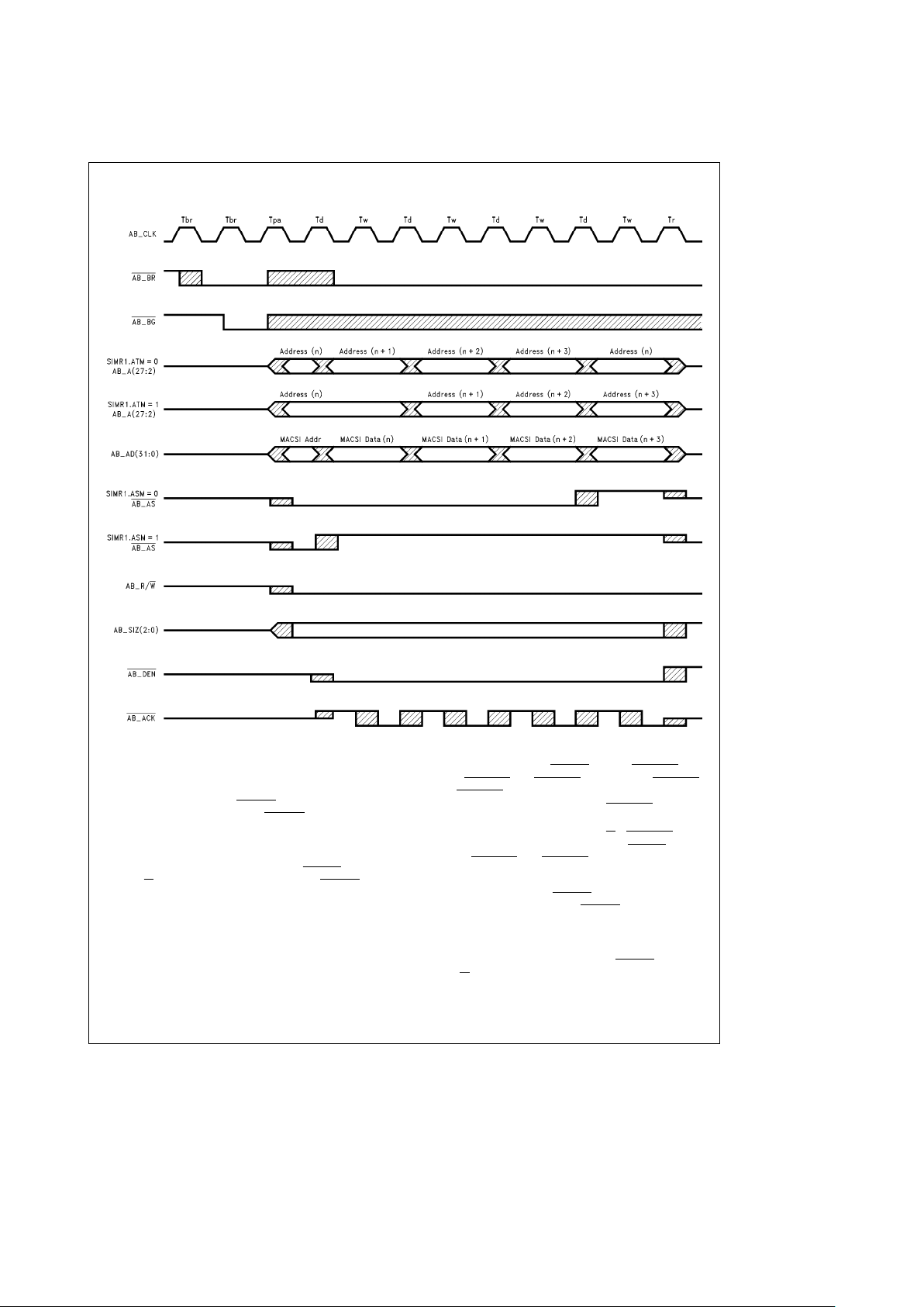
6.0 Functional Description (Service Engine) (Continued)
TL/F/11705– 12
FIGURE 6-7. ABus Burst Write: Physical AddressingÐ16 Bytes, 1 w/s
6.4.4 Virtual Addressing Bus Transactions
Single Read
Tbr: MACSI device asserts ABÐBR
to indicate it wishes to
perform a transfer. Host asserts ABÐBG
. The MACSI device moves to Tva within the next three clocks, and then
drives ABÐA and ABÐAD.
Tva: MACSI device drives ABÐA and ABÐAD with the virtual address for one clock, negates ABÐAS
, asserts
ABÐR/W
, drives ABÐSIZ[2:0], and negates ABÐBR if an-
other transaction is not required.
Tmmu: Host MMU performs an address translation during
this clock.
Tpa: Host MMU drives ABÐAD with the translated (physical) address.
Td: MACSI device negates ABÐAS
, asserts ABÐDEN, and
samples ABÐACK
and ABÐERR. Slave asserts ABÐACK,
drives ABÐERR
, and drives ABÐAD (with data) when
ready. MACSI device samples a valid ABÐACK
, and cap-
tures the read data. Tw states may occur after Td.
Tr: MACSI device negates ABÐR/W
,ABÐDEN, and
ABÐSIZ[2:0], and releases ABÐA and ABÐAS
. Slave
deasserts ABÐACK
and ABÐERR and releases ABÐAD.
Single Write
Tbr: MACSI device asserts ABÐBR
to indicate it wishes to
perform a transfer. Host asserts ABÐBG
. The MACSI device moves to Tva within the next three clocks, and then
drives ABÐA and ABÐAD.
Tva: MACSI device drives ABÐA and ABÐAD with the virtual address for one clock, negates ABÐAS
, negates
ABÐR/W
, and drives ABÐSIZ[2:0].
38

6.0 Functional Description (Service Engine) (Continued)
Tmmu: Host MMU performs an address translation during
this clock.
Tpa: Host MMU drives ABÐAD with the address.
Td: MACSI device negates ABÐAS
, asserts ABÐDEN,
drives ABÐAD with the write data and starts sampling
ABÐACK
and ABÐERR. Slave captures ABÐAD data, as-
serts ABÐACK
, and drives ABÐERR. MACSI device sam-
ples a valid ABÐACK
. Tw states may occur after Td.
Tr: MACSI device negates ABÐR/W,ABÐDEN, and
ABÐSIZ[2:0], and releases ABÐA, ABÐAD, and ABÐAS
.
Slave deasserts ABÐACK
and ABÐERR and stops driving
ABÐAD with data.
Burst Read
Tbr: MACSI device asserts ABÐBR
to indicate it wishes to
perform a transfer. Host asserts ABÐBG
. The MACSI device moves to Tva within the next three clocks, and then
drives ABÐA and ABÐAD.
Tva: MACSI device drives ABÐA and ABÐAD with the virtual address for one clock, negates ABÐAS
, asserts
ABÐR/W
, drives ABÐSIZ[2:0], and negates ABÐBR if an-
other transaction is not required.
Tmmu: Host MMU performs an address translation during
this clock.
Tpa: Host MMU drives ABÐAD with the translated (physical) address.
Td: MACSI device asserts ABÐDEN
and samples
ABÐACK
and ABÐERR. Slave asserts ABÐACK, drives
ABÐERR
, and drives ABÐAD (with data) when ready.
MACSI device samples a valid ABÐACK
, and captures the
read data. Tw states may occur after Td. This state is repeated four or eight times (according to burst size). If
SIMR1.ASM
e
0 the MACSI device negates ABÐAS in the
last Td cycle. If SIMR1.ASM
e
1, the MACSI device will
negate ABÐAS
in the first Td cycle.
Tr: MACSI device negates ABÐR/W,ABÐDEN, and
ABÐSIZ[2:0], and releases ABÐA and ABÐAS
. Slave
deasserts ABÐACK
and ABÐERR and releases ABÐAD.
Burst Write
Tbr: MACSI device asserts ABÐBR
to indicate it wishes to
perform a transfer. Host asserts ABÐBG
. The MACSI device moves to Tva within the next three clocks, and then
drives ABÐA and ABÐAD.
Tva: MACSI device drives ABÐA and ABÐAD with the virtual address for one clock, negates ABÐAS
, negates
ABÐR/W
, drives ABÐSIZ[2:0].
Tmmu: Host MMU performs an address translation during
this clock.
Tpa: Host MMU drives ABÐAD with the address.
Td: MACSI device asserts ABÐDEN
, drives ABÐAD with
the write data, and starts sampling ABÐACK
and
ABÐERR
. Slave captures ABÐAD data, asserts ABÐACK
and drives ABÐERR. MACSI device samples a valid
ABÐACK
. Tw states may occur after Td. Td is repeated as
required for the complete burst. If SIMR1.ASM
e
0, the
MACSI device negates ABÐAS
in the last Td cycle. If
SIMR1.ASM
e
1, the MACSI device will negate ABÐAS in
the first Td cycle.
Tr: MACSI device negates ABÐR/W
,ABÐDEN, and
ABÐSIZ[2:0], releases ABÐA, ABÐAD, and ABÐAS
, and
stops driving ABÐAD with data. Slave deasserts ABÐACK
and ABÐERR.
6.5 ENHANCED ABUS MODE
When the enhanced ABus mode is selected, several changes occur. The timing of ABÐACK
is modified during read
accesses. In this mode, read data is expected one cycle
after the ABÐACK
signal (see
Figure 6-8
and
Figure 6-11
).
In addition, channel information is no longer supplied on the
upper four bits of the Address/Data lines during the address
cycle. Instead, the value of this nibble of address is supplied
from a programmable register within the MACSI device (for
a full description of these bits please see System Interface
Mode Register1 (SIMR1)). Finally, the ABÐDEN
signal becomes an input in this enhanced mode. This signal, along
with ABÐACK
and ABÐERR, are used to encode a subset
of the acknowledge, retry, and error functions supported on
the SBus.
These enhancements make it easier to connect the MACSI
device to the SBus as a bus master. However, a full FDDI
adapter design requires the design of a slave interface from
the SBus to the control bus of the MACSI device and the
other FDDI components.
6.5.1 Enhanced ABus Mode Bus Transactions
Bus transactions in the Enhanced Abus Mode are shown in
Figure 6-8
through
Figure 6-11.
In the Enhanced ABus
mode, the Bus Request signal (ABÐBR
) will be deasserted
after the bus is granted until the completion of the bus transaction. The only exception to this may occur when the
MACSI device is attempting back-to-back burst reads. In
this case ABÐBR
may be deasserted for as few as two
cycles.
Single Read
Tbr: MACSI device asserts ABÐBR
to indicate it wishes to
perform a transfer. Host asserts ABÐBG
. The MACSI de-
vice moves to Tma on the next cycle.
Tma: MACSI device drives ABÐA and ABÐAD with the
master address, asserts ABÐAS
, drives ABÐR/W and
ABÐSIZ[2:0], and negates ABÐBR
until the end of this
transaction.
Tpa: The Physical address is asserted by the MMU.
Td: MACSI device negates ABÐAS
and samples ABÐACK,
ABÐERR
, and ABÐDEN. Slave asserts ABÐACK,
ABÐERR
, and ABÐDEN with the appropriate acknowledgment. The MACSI device samples a valid acknowledgment
and moves to Tr. Tw states may occur after Td.
Tr: MACSI device negates ABÐR/W
,ABÐDEN, and
ABÐSIZ[2:0], releases ABÐA and ABÐAS
, and samples
ABÐAD. Slave drives ABÐAD (with data), deasserts
ABÐACK
,ABÐERR, and ABÐDEN, and releases AB
Ð
AD.
39

6.0 Functional Description (Service Engine) (Continued)
TL/F/11705– 13
FIGURE 6-8. Enhanced ABus Read TimingÐ0 w/s, 1 w/s
TL/F/11705– 14
FIGURE 6-9. Enhanced ABus Mode Write Timing
40

6.0 Functional Description (Service Engine) (Continued)
TL/F/11705– 15
FIGURE 6-10. Enhanced ABus Mode Burst Write Timing
Single Write
Tbr: MACSI device asserts ABÐBR
to indicate it wishes to
perform a transfer. Host asserts ABÐBG
. The MACSI de-
vice moves to Tma in the next cycle.
Tma: MACSI device drives ABÐA and ABÐAD with the
master address, asserts ABÐAS
, drives ABÐR/W and
ABÐSIZ[2:0], and negates ABÐBR
until the end of this
transaction.
Tpa: The Physical address is asserted by the MMU.
Td: MACSI device negates ABÐAS
, drives ABÐAD with the
write data and starts sampling ABÐACK
,ABÐERR, and
ABÐDEN
. Slave captures ABÐAD data, and acknowledges
with ABÐACK
,ABÐERR, and ABÐDEN. Tw states may
occur after Td if the slave does not acknowledge.
Tr: MACSI device negates ABÐR/W
,ABÐSIZ[2:0], releas-
es ABÐA, ABÐAD, and ABÐAS
, and stops driving
ABÐAD with data. Slave deasserts ABÐACK
,ABÐERR,
and ABÐDEN
.
41

6.0 Functional Description (Service Engine) (Continued)
TL/F/11705– 16
FIGURE 6-11. Enhanced ABus Mode Back-to-Back Read Timing
Burst Read
Tbr: MACSI device asserts ABÐBR
to indicate it wishes to
perform a transfer. Host asserts ABÐBG
. The MACSI device moves to Tma in the next cycle. This cycle may be
skipped if ABÐBR was asserted during the previous access. This allows for back-to-back burst reads.
Tma: MACSI device drives ABÐA and ABÐAD with the
master address, asserts ABÐAS
, drives ABÐR/W and
ABÐSIZ[2:0], and negates ABÐBR
for at least two cycles.
Tpa: The Physical Address is asserted by the MMU.
Td: MACSI device samples ABÐACK
,ABÐERR, and
ABÐDEN
, and increments the address on ABÐA. Slave
acknowledges using ABÐACK
,ABÐERR, and ADÐDEN.
MACSI device samples a valid ABÐACK
and latches data
in the following cycle. Tw states may occur after Td. Td
state is repeated four or eight times (according to the burst
size). If SIMR1.ASM
e
0, the MACSI device negates
ABÐAS
in the last Td cycle. If SIMR1.ASMe1, the MACSI
device negates ABÐAS
in the first Td cycle.
Tr: MACSI device negates ABÐR/W and ABÐSIZ[2:0]and
releases ABÐA and ABÐAS
. Slave drives ABÐAD (with
data), deasserts ABÐACK
,ABÐERR, and ABÐDEN.Ifan-
other request is pending (ABÐBR
asserted) and the Bus is
regranted in this cycle, the MACSI device will proceed directly to the Tma state of the next burst. The normal Tbr
state is skipped allowing back-to-back burst reads.
Burst Write
Tbr: MACSI device asserts ABÐBR
to indicate it wishes to
perform a transfer. Host asserts ABÐBG
. The MACSI de-
vice moves to Tma in the next cycle.
Tma: MACSI device drives ABÐA and ABÐAD with the
master address, asserts ABÐAS
, drives ABÐR/W and
ABÐSIZ[2:0], and negates ABÐBR
until this transaction is
completed.
Tpa: The Physical Address is asserted by the MMU.
Td: MACSI device drives ABÐAD with the write data, samples ABÐACK
,ABÐERR, and ABÐDEN, and increments
the address on ABÐA. Slave captures ABÐAD data and
acknowledges using ABÐACK
,ABÐERR, and ABÐDEN.
MACSI device samples a valid acknowledge. Tw states may
occur after Td. Td state is repeated as required for the complete burst. If SIMR1.ASM
e
0, the MACSI device negates
ABÐAS
in the last Td cycle. If SIMR1.ASMe1, the MACSI
device negates ABÐAS
in the first Td cycle.
Tr: MACSI device negates ABÐR/W,ABÐSIZ[2:0], releases ABÐA and ABÐAS
, and stops driving ABÐAD with
data. Slave deasserts ABÐACK
,ABÐERR, and ABÐDEN.
42

7.0 Control Information
7.1 OVERVIEW
The Control Information includes Operation, Event, Status
and Parameter Registers that are used to manage and operate the MACSI Device. A controller on the external Control Bus gains access to read and write these parameters
via the Control Bus Interface.
The MACSI device combines the functions of the original
DP83261 BMAC device and the DP83265 BSI device with
many enhanced capabilities. The MACSI device has additional Control Bus address lines compared to the BMAC and
BSI devices (CBA(8:0)). When the most significant address
bit (CBA8) is zero, the internal BMAC register block is se-
lected. When CBA8 is 1, the internal BSI register block is
selected. The actual addresses within the MACSI device are
defined in Table 7-1 and Table 7-2.
All registers and control bits within the BSI register block of
the MACSI device have the same relative addresses and
functions as they do in the BSI device. All registers and
control bits within the BMAC register block of the MACSI
device have the same relative addresses and functions as
they do in the BMAC device. The only exceptions to this are
shown in the detailed register descriptions following the
memory map table. There are two registers which have new
features unique to the MACSI device or functions which are
slightly modified from the original BMAC or BSI device.
These are MCMR0 and MCMR2.
TABLE 7-1. MACSI Memory Map (BMAC Registers)
Address Register Name
Access Rules
Reset
Value
Read Write
000 MAC Mode Register 0 (MCMR0) Always Always 00
001 Option Register (Option) Always Always 00
002 Function Register (Function) Always Always 00
003 Reserved N/A N/A
004 Reserved N/A N/A
005 MAC Mode Register 2 (MCMR2) Always Always 00
006 Reserved N/A N/A
007 MAC Revision (MCRev) Always Data Ignored *
008 MAC Compare Register (MCCMP) Always Always 00
009–00B Reserved N/A N/A
00C Current Receiver Status Register (CRS0) Always Data Ignored 00
00D Reserved N/A N/A
00E Current Transmitter Status Register (CTS0) Always Data Ignored 00
00F Reserved N/A N/A
010 Ring Event Latch Register 0 (RELR0) Always Conditional 00
011 Ring Event Mask Register 0 (REMR0) Always Always 00
012 Ring Event Latch Register 1 (RELR1) Always Conditional 00
013 Ring Event Mask Register 1 (REMR1) Always Always 00
014 Token and Timer Event Latch Register (TELR0) Always Conditional 00
015 Token and Timer Event Mask Register (TEMR0) Always Always 00
016–017 Reserved N/A N/A
018 Counter Increment Latch Register (CILR) Always Conditional 00
019 Counter Increment Mask Register (CIMR) Always Always 00
01A–01B Reserved N/A N/A
01C Counter Overflow Latch Register (COLR) Always Conditional 00
01D Counter Overflow Mask Register (COMR) Always Always 00
01E–027 Reserved N/A N/A
43

7.0 Control Information (Continued)
TABLE 7-1. MACSI Memory Map (BMAC Registers) (Continued)
Address Register Name
Access Rules
Reset
Value
Read Write
028 Internal Event Latch Register (IELR) Always Conditional 00
029–02B Reserved N/A N/A
02C Exception Status Register (ESR) Always Conditional 00
02D Exception Mask Register (EMR) Always Always 00
02E Interrupt Condition Register (ICR) Always Data Ignored 00
02F Interrupt Mask Register (IMR) Always Always 00
030–03F Reserved N/A N/A
040–07F MAC Parameters Stop Mode Stop Mode NA
080–0BF Counters/Timers Always Stop Mode NA
0C0-0FF Reserved N/A N/A
*eContains a MAC Revision code.
NA
e
Not altered upon reset.
N/A
e
Not Applicable
Table 7-2. MACSI Memory Map (BSI Registers)
Address Register Name
Access Rules
Reset
Value
Read Write
100 System Interface Mode Register 0 (SIMR0) Always Always 00
101 System Interface Mode Register 1 (SIMR1) Always Always 00
102 Pointer RAM Control and Address Register (PCAR) Always Always NA
103 Mailbox Address Register (MBAR) Always Always
²
104 Master Attention Register (MAR) Always Data Ignored 00
105 Master Notify Register (MNR) Always Always 00
106 State Attention Register (STAR) Always Conditional 07
107 State Notify Register (STNR) Always Always 00
108 Service Attention Register (SAR) Always Conditional 0F
109 Service Notify Register (SNR) Always Always 00
10A No Space Attention Register (NSAR) Always Conditional FF
10B No Space Notify Register (NSNR) Always Always 00
10C Limit Address Register (LAR) Always Always NA
10D Limit Data Register (LDR) Always Always NA
10E Request Attention Register (RAR) Always Conditional 00
10F Request Notify Register (RNR) Always Always 00
110 Request Channel 0 Configuration Register 0 (R0CR0) Always Always NA
111 Request Channel 1 Configuration Register 0 (R1CR0) Always Always NA
112 Request Channel 0 Expected Frame Status Register (R0EFSR) Always Always NA
113 Request Channel 1 Expected Frame Status Register (R1EFSR) Always Always NA
44

7.0 Control Information (Continued)
Table 7-2. MACSI Memory Map (BSI Registers)
Address Register Name
Access Rules
Reset
Value
Read Write
114 Indicate Attention Register (IAR) Always Conditional 00
115 Indicate Notify Register (INR) Always Always 00
116 Indicate Threshold Register (ITR) Always INSTOP Mode NA
or EXC
e
1 Only
117 Indicate Mode Configuration Register (IMCR) Always INSTOP Mode NA
Only
118 Indicate Copy Configuration Register (ICCR) Always Always NA
119 Indicate Header Length Register (IHLR) Always INSTOP Mode NA
or EXC
e
1 Only
11A Address Configuration Register (ACR) Always Always 00
11B Request Channel 0 Configuration Register 1 (R0CR1) Always Always 00
11C Request Channel 1 Configuration Register 1 (R1CR1) Always Always 00
11D–11E Reserved N/A N/A
11F System Interface Compare Register (SICMP) Always Always NA
120–1FF Reserved N/A N/A
²
e
Initialized to a System Interface Revision code upon reset. The System Interface Revision code remains until it is overwritten by the host.
NA
e
Not altered upon reset.
N/A
e
Not Applicable
The MAC Control Information Address Space is divided into
4 groups as shown in Table 7-3. An information summary is
given for each group followed by a detailed description of all
registers.
#
MAC Operation Registers (Table 7-4)
#
MAC Event Registers (Table 7-5)
#
MAC Parameters (Table 7-6)
#
MAC Counters/Timers (Table 7-7)
The System Interface Operation registers are accessed directly via the Control Bus. Limit RAM Registers are accessed indirectly via the Control Bus using the Limit RAM
Data and Limit RAM Address Registers. The Pointer RAM
Registers are accessed indirectly via the Control Bus and
ABus using the Pointer RAM Address and Control Register,
the Mailbox Address Register, and a mailbox location in
ABus memory. Descriptors are fetched (or written) by the
MACSI device across the ABus.
#
System Interface Registers (Table 7-8)
7.2 CONVENTIONS
When referring to multi-byte fields, byte 0 is always the most
significant byte. When referring to bits within a byte, bit (7) is
the most significant bit and bit (0) is the least significant bit.
When referring to the contents of a byte, the most significant bit is always referred to first. When referring to a bit
within a byte the notation registerÐname.bitÐname is
used. For example, MCMR0.RUN references the RUN bit in
MAC Mode Register 0.
45

7.0 Control Information (Continued)
TABLE 7-3. MAC Control Information Address Space
Address
Description
Read Write
Range Conditions Conditions
000–007 Operation Registers Always (Note 2) Always (Note 2)
008–02F Event Registers Always (Note 2) Always (cond) (Note 2)
030–03F Reserved N/A (Note 4) N/A (Note 4)
040–07F MAC Parameters Stop Mode Stop Mode
(Notes 1, 3) (Notes 1, 3)
080-0BF Counters/Timers Always Stop Mode (Note 1)
0C0-0FF Reserved N/A (Note 4) N/A (Note 4)
Note 1: An attempt to access a currently inaccessible MAC Control location because of the current
mode or because it is a reserved address space will cause a command error (bit CCE of the
Exception Status Register is set to One).
Note 2: Read and write accesses to reserved locations within the Operation and Event Address
ranges of the MAC Control Information Space cause a command error (bit CCE of the Exception
Status Register is set to One).
Note 3: The MAC Parameter RAM is also accessible when conditions a, b and c are true. Otherwise accesses will cause a command error (bit CCE of the Exception Status Register is set to One)
and the access will not be performed.
a) The MAC Transmitter is in state T0 or T1 or T3;
b) Option.ITC
e
1 and Option.IRRe1
c) Function.BCN
e
0 and Function.CLMe0
Note 4: Reserved bits in registers are always read as 0 and are not writable.
TABLE 7-4. MAC Operation Registers
Addr Name D7 D6 D5 D4 D3 D2 D1 D0 Read Write
000 MCMR0 DIAG ILB RES RES PIP MRP CBP RUN Always Always
001 Option ITC EMIND IFCS IRPT IRR ITR ELA ESA Always Always
002 Function RES RES RES CLM BCN MCRST RES MARST Always Always
003–004 Reserved RES RES RES RES RES RES RES RES N/A N/A
005 MCMR2 RES RES RES AFIE LLC MCE SMT MCE RES BOSEL Always Always
006 Reserved RES RES RES RES RES RES RES RES N/A N/A
007 MCRev REV(7–0) Always Ignored
Note 1: Attempts to access reserved locations within the MAC Operation Registers will result in Command Rejects (ESR.CCE set to ONE).
Note 2: On Master Reset, all MAC Operation Registers are set to Zero except the Revision Register.
46

7.0 Control Information (Continued)
TABLE 7-5. MAC Event Registers
Addr Name D7 D6 D5 D4 D3 D2 D1 D0 Read Write
008 MCCMP MCCMP(7– 0) Always Always
009–00B Reserved RES RES RES RES RES RES RES RES N/A N/A
00C CRS0 RFLG RS2 RS1 RS0 RES RTS2 RTS1 RTS0 Always Ignored
00D Reserved RES RES RES RES RES RES RES RES N/A N/A
00E CTS0 ROP TS2 TS1 TS0 TTS3 TTS2 TTS1 TTS0 Always Ignored
00F Reserved RES RES RES RES RES RES RES RES N/A N/A
010 RELR0 RES DUP ADD PINV OTR MAC CLMR BCNR RNOP ROP Always Conditional
011 REMR0 RES DUP ADD PINV OTR MAC CLMR BCNR RNOP ROP Always Always
012 RELR1 LOCLM HICLM MYCLM RES RES RES MYBCN OTRBCN Always Conditional
013 REMR1 LOCLM HICLM MYCLM RES RES RES MYBCN OTRBCN Always Always
014 TELR0 RLVD TKPASS TKCAPT CBERR DUPTKR TRTEXP TVXEXP ENTRMD Always Conditional
015 TEMR0 RLVD TKPASS TKCAPT CBERR DUPTKR TRTEXP TVXEXP ENTRMD Always Always
016–017 Reserved RES RES RES RES RES RES RES RES N/A N/A
018 CILR RES TK RCVD FR TRX FR NCOP FR COP FR LST FREI FR RCV Always Conditional
019 CIMR RES TK RCVD FR TRX FR NCOP FR COP FR LST FREI FR RCV Always Always
01A–01B Reserved RES RES RES RES RES RES RES RES N/A N/A
01C COLR RES TK RCVD FR TRX FR NCOP FR COP FR LST FREI FR RCV Always Conditional
01D COMR RES TK RCVD FR TRX FR NCOP FR COP FR LST FREI FR RCV Always Always
01E–027 Reserved RES RES RES RES RES RES RES RES N/A N/A
028 IELR RES RES RES RES TSM ERR RSM ERR RES MPE Always Conditional
029–02B Reserved RES RES RES RES RES RES RES RES N/A N/A
02C ESR CWI CCE CPE RES RES RES RES PPE Always Conditional
02D EMR ZERO CCE CPE RES RES RES RES PPE Always Always
02E ICR ESE IERR RES RES COE CIE TTE RNG Always Ignored
02F IMR ESE IERR RES RES COE CIE TTE RNG Always Always
030–03F Reserved RES RES RES RES RES RES RES RES N/A N/A
Note 1: Attempts to access reserved locations within the MAC Event Registers will result in Command Rejects (ESR.CCE set to ONE).
Note 2: Bits in the conditional write registers are only written when the corresponding bit in the Compare Register is equal to the bit to be overwritten.
Note 3: On Master Reset all Event Registers are reset to Zero.
7.3 ACCESS RULES
For the Ring Engine (MAC), all Control Interface accesses
are checked against the current operational mode to determine if the register is currently accessible. If not currently
accessible, the Control Bus Interface access is rejected
(and reported in an Event Register). This means that the
Control Bus Interface completes all accesses in a deterministic amount of time. Certain Status and Parameter registers are not accessible while in Run mode because the Ring
Engine might access those locations. The Exception
Status Register can be checked to verify that the operation
terminated normally.
The Service Engine Registers are always accessible.
7.3.1 MAC Parameter RAM
The MAC parameter RAM is accessible in Stop mode and in
RUN mode while: the MAC Transmitter is in states T0, T1 or
T3; Option.ITC and Option.IRR are set; and Function.BCN
and Function.CLM are not set. Otherwise a command reject
is given (ESR.CCE) and the Parameter RAM will not be read
or written.
47

7.0 Control Information (Continued)
TABLE 7-6. MAC Parameter RAM
Addr Name Register Contents
040 MLA0 MLA(47– 40)
041 MLA1 MLA(39– 32)
042 MLA2 MLA(31– 24)
043 MLA3 MLA(23– 16)
044 MLA4 MLA(15– 8)
045 MLA5 MLA(7– 0)
046 MSA0 MSA(15 –8)
047 MSA1 MSA(7 –0)
048 GLA0 GLA(47 –40)
049 GLA1 GLA(39 –32)
04A GLA2 GLA(31 – 24)
04B GLA3 GLA(23 – 16)
04C GLA4 GLA(15 – 8)
04D Reserved
04E GSA0 GSA(15– 8)
04F Reserved
050 TREQ0 TREQ(31 –24)
051 TREQ1 TREQ(23 –16)
052 TREQ2 TREQ(15 –8)
053 TREQ3 TREQ(7 –0)
054 TBT0 TBT(31– 24)
055 TBT1 TBT(23– 16)
056 TBT2 TBT(15– 8)
057 TBT3 TBT(7– 0)
058 FGM0 FGM(7– 0)
059 FGM1 FGM(F– 8)
05A0–5F Reserved
060 PGM10 PGM(87– 80)
061 PGM11 PGM(8F– 88)
062 PGM12 PGM(97– 90)
Addr Name Register Contents
063 PGM13 PGM(9F –98)
064 PGM14 PGM(A7 –A0)
065 PGM15 PGM(AF –A8)
066 PGM16 PGM(B7 –B0)
067 PGM17 PGM(BF –B8)
068 PGM18 PGM(C7 –C0)
069 PGM19 PGM(CF –C8)
06A PGM1A PGM(D7– D0)
06B PGM1B PGM(DF– D8)
06C PGM1C PGM(E7 –E0)
06D PGM1D PGM(EF–E8)
06E PGM1E PGM(F7– F0)
06F PGM1F PGM(FF –F8)
070 PGM0 PGM(7– 0)
071 PGM1 PGM(F– 8)
072 PGM2 PGM(17– 10)
073 PGM3 PGM(1F– 18)
074 PGM4 PGM(27– 20)
075 PGM5 PGM(2F– 28)
076 PGM6 PGM(37– 30)
077 PGM7 PGM(3F– 38)
078 PGM8 PGM(47– 40)
079 PGM9 PGM(4F– 48)
07A PGMA PGM(57 – 50)
07B PGMB PGM(5F – 58)
07C PGMC PGM(67 –60)
07D PGMD PGM(6F–68)
07E PGME PGM(77– 70)
07F PGMF PGM(7F –78)
7.3.2 MAC Counters/Timer Thresholds
The MAC event counters and timer thresholds are always
readable, and are writable in Stop mode.
48

7.0 Control Information (Continued)
TABLE 7-7. MAC Counters and Timer Thresholds
Addr Name Register Contents
080–086 Reserved
087 THSH1 Null(7 – 4), THSH1(3 – 0)
088–092 Reserved
093 TMAX Null(7 –4), TMAX(3 – 0)
094–096 Reserved
097 TVX Null(7– 4), TVX(3 –0)
098 TNEG0 TNEG(31–24)
099 TNEG1 TNEG(23–16)
09A TNEG2 TNEG(15– 8)
09B TNEG3 TNEG(7– 0)
09C–09E Reserved
09F LTCT LTCT(7 –0)
0A0 FRCT0 Zero(31 – 24)
0A1 FRCT1 Null(7 – 4), FRCT(19– 16)
0A2 FRCT2 FRCT(15 – 8)
0A3 FRCT3 FRCT(7 – 0)
0A4 EICT0 Zero(31– 24)
0A5 EICT1 Null(7– 4), EICT(19–16)
0A6 EICT2 EICT(15– 8)
0A7 EICT3 EICT(7– 0)
0A8 LFCT0 Zero(31 –24)
0A9 LFCT1 Null(7 –4), LFCT(19 – 16)
0AA LFCT2 LFCT(15–8)
0AB LFCT3 LFCT(7–0)
0AC FCCT0 Zero(31 –24)
0AD FCCT1 Null(7 –4), FCCT(19 – 16)
0AE FCCT2 FCCT(15 – 8)
0AF FCCT3 FCCT(7 – 0)
Addr Name Register Contents
0B0 FNCT0 Zero(31 –24)
0B1 FNCT1 Null(7 –4), FNCT(19 – 16)
0B2 FNCT2 FNCT(15 –8)
0B3 FNCT3 FNCT(7 –0)
0B4 FTCT0 Zero(31– 24)
0B5 FTCT1 Null(7– 4), FTCT(19–16)
0B6 FTCT2 FTCT(15– 8)
0B7 FTCT3 FTCT(7– 0)
0B8 TKCT0 Zero(31 – 24)
0B9 TKCT1 Null(7 – 4), TKCT(19– 16)
0BA TKCT2 TKCT(15 –8)
0BB TKCT3 TKCT(7 –0)
0BC RLCT0 Zero(31–24)
0BD RLCT1 Null(7–4), RLCT(19 – 16)
0BE RLCT2 RLCT(15 –8)
0BF RLCT3 RLCT(7 –0)
Note 1: Null(7– 4) indicates that these bits are forced to zero on reads, and
are ignored on writes.
Note 2: The value obtained on reads from reserved locations is not specified.
Note 3: On Master Reset, the event counters are not cleared.
The event counters are 20-bit counters and are read
through three control accesses. In order to guarantee a
consistent snapshot, whenever byte 3 of an event counter is
read, byte 1 and byte 2 of the counters are loaded into a
holding register. Byte 1 and byte 2 may then be read from
the holding register. A single holding register is shared by all
of the counters but (for convenience) is accessible at several places within the address space. Consistent readings
across counters can be accomplished using the Counter
Increment Latch Register (CILR).
The event counters are not reset as a result of a Master
Reset. This may be done by either reading the counters out
and keeping track relative to the initial value read, or by
writing a value to all of the counters in stop mode. The
counters may be written in any order. With some exceptions, interrupts are available when the counters increment
or wraparound.
49

7.0 Control Information (Continued)
System Interface Registers
TABLE 7-8. System Interface Registers
Addr Name D7 D6 D5 D4 D3 D2 D1 D0 Read Write
100 SIMR0 SMLB SMLQ VIRT BIGEND FLOW MRST FABCLK TEST Always Always
101 SIMR1 ABÐA31 ABÐA30 ABÐA29 ABÐA28 ATM ASM RES EAM Always Always
102 PCAR BP1 BP0 PTRW A4 A3 A2 A1 A0 Always Always
103 MBAR Mailbox Address[27:24],[23:16],[15:8],[7:0
]
Always Always
104 MAR STA NSA SVA RQA INA RES RES RES Always Ignored
105 MNR STAN NSAN SVAN RQAN INAN RES RES RES Always Always
106 STAR ERR BPE CPE CWI CMDE SPSTOP RQSTOP INSTOP Always Conditional
107 STNR ERRN BPEN CPEN CWIN CMDEN SPSTOPN RQSTOPN INSTOPN Always Always
108 SAR RES RES RES RES ABR0 ABR1 LMOP PTOP Always Conditional
109 SNR RES RES RES RES ABR0N ABR1N LMOPN PTOPN Always Always
10A NSAR NSR0 NSR1 LDI0 NSI0 LDI1 NSI1 LDI2 NSI2 Always Conditional
10B NSNR NSR0N NSR1N LDI0N NSI0N LDI1N NSI1N LDI2N NSI2N Always Always
10C LAR LRA3 LRA2 LRA1 LRA0 LMRW RES RES LRD8 Always Always
10D LDR LRD7 LRD6 LRD5 LRD4 LRD3 LRD2 LRD1 LRD0 Always Always
10E RAR USRR0 RCMR0 EXCR0 BRKR0 USRR1 RCMR1 EXCR1 BRKR1 Always Conditional
10F RNR USRR0N RCMR0N EXCR0N BRKR0N USRR1N RCMR1N EXCR1N BRKR1N Always Always
110 R0CR0 TT1 TT0 PRE HLD FCT SAT VST FCS Always Always
111 R1CR0 TT1 TT0 PRE HLD FCT SAT VST FCS Always Always
112 R0EFSR VDL VFCS EE1 EE0 EA1 EA0 EC1 EC0 Always Always
113 R1EFSR VDL VFCS EE1 EE0 EA1 EA0 EC1 EC0 Always Always
114 IAR RES RES EXCI0 BRKI0 EXCI1 BRKI1 EXCI2 BRKI2 Always Conditional
115 INR RES RES EXC0N BRK0N EXC1N BRK1N EXC2N BRK2N Always Always
116 ITR THR7 THR6 THR5 THR4 THR3 THR2 THR1 THR0 Always INSTOPe1or
EXC
e
1 Only
117 IMCR SM1 SM0 SKIP FPP BOT2 BOT1 BOB BOS Always INSTOPe1 Only
118 ICCR CC0 RES CC1 RES CC2 Always Always
119 IHLR HL7 HL6 HL5 HL4 HL3 HL2 HL1 HL0 Always INSTOPe1or
EXCe1 Only
11A ACR PCKI2 PCKI1 PCKI0 RSWP1 RSWP0 ISWP2 ISWP1 ISWP0 Always Always
11B R0CR1 EFT RES RES RES RES RES RES ETR Always Always
11C R1CR1 EFT RES RES RES RES RES RES ETR Always Always
11D–11E Reserved RES RES RES RES RES RES RES RES N/A N/A
11F SICMP CMP7 CMP6 CMP5 CMP4 CMP3 CMP2 CMP1 CMP0 Always Always
120–1FF Reserved RES RES RES RES RES RES RES RES N/A N/A
Note: Bits in the conditional write registers are only written when the corresponding bit in the System Interface Compare Register is equal to the bit to be
overwritten.
50

7.0 Control Information (Continued)
Control Registers
The Control Registers are used to configure and control the
operation of the MACSI device.
The Control Registers include the following registers:
#
MAC Mode Registers (MCMR2 –0) establish the major
operating parameters for the MAC portion of the MACSI
device.
#
Option Register (Option) selects major configuration
options for the MAC portion of the device.
#
Function Register (Function) initiates major MAC level
functions.
#
MAC Revision (MCRev) this register contains the silicon
revision code for the MAC state machines of this device.
#
System Interface Mode Registers (SIMR1 –0) establishes major operating parameters for the System Interface.
#
Pointer RAM Control and Address Register (PCAR) is
used to program the parameters for the PTOP (Pointer
RAM Operation) service function.
#
Mailbox Address Register (MBAR) is used to program
the memory address of the mailbox used in the data
transfer of the PTOP service function.
#
Limit Address Register (LAR) is used to program the
parameters and data used in the LMOP (Limit RAM Operation) service function.
#
Limit Data Register (LDR) is used to program the data
used in the LMOP service function.
#
Request Channel 0 Configuration Registers (R0CR1 –
0) are used to program the operational parameters for
Request Channel 0.
#
Request Channel 1 Configuration Registers (R1CR1 –
0) are used to program the operational parameters for
Request Channel 1.
#
Request Channel 0 Expected Frame Status Register
(R0EFSR) defines the expected frame status for frames
being confirmed on Request Channel 0.
#
Request Channel 1 Expected Frame Status Register
(R1EFSR) defines the expected frame status for frames
being confirmed on Request Channel 1.
#
Indicate Threshold Register (ITR) is used to specify a
maximum number of frames that can be copied onto an
Indicate Channel before a breakpoint is generated.
#
Indicate Mode Configuration Register (IMCR) specifies how the incoming frames are sorted onto Indicate
Channels, enables frame filtering, and enables breakpoints on various burst boundaries.
#
Indicate Copy Configuration Register (ICCR) is used
to program the copy criteria for each of the Indicate
Channels.
#
Indicate Header Length Register (IHLR) defines the
length of the frame header for use with the Header/Info
Sort Mode.
Event Registers
The Event Registers record the occurrence of events or
series of events. Events are recorded and contribute to generating Interrupt signals. There is a two-level hierarchy in
generating this signal, as shown in
Figure 7-1.
TL/F/11705– 17
FIGURE 7-1. Event Registers Hierarchy
51

7.0 Control Information (Continued)
The MACSI device has two interrupts signals. One provides
interrupts on those events generated by the MAC state machines (INT0
) and the other provides interrupts on those
events generated by the System Interface state machines
(INT1
). This partition maintains hardware and software compatibility with earlier designs based on the BMAC and BSI
devices.
At the first level of the hierarchy, events are recorded as bits
in the Attention Registers (e.g., No Space Attention Register). Each Attention Register has a corresponding Notify
Register (e.g., No Space Notify Register). When a bit in the
Attention Register is set to One and its corresponding bit in
the Notify Register is also set to One, the corresponding bit
in the Master Attention Register will be set to one.
At the second level of the hierarchy, if a bit in the Master
Attention Register is set to One and the corresponding bit in
the Master Notify Register is set to One, the Interrupt signal
is asserted.
To ensure that events are not missed when updating the
attention registers, all attention registers are conditional
write registers. Bits in Conditional Write Registers (e.g., No
Space Attention Register) are only written when the corresponding bits in the Compare Register are equal to the bits
to be overwritten. Read operations for conditional write registers automatically cause the Compare Register to be loaded with the contents of the conditional write register being
accessed. The MACSI device contains two compare registers. One is used for Ring Engine Event Registers (MCCMP)
and the other is used for System Interface Event Registers
(SICMP).
Events are recorded in Attention Registers and contribute to
the Interrupt when the bit in the corresponding Notify Register is set (see
Figure 7-1
). Bits in the Master Attention Register (MAR) are not cleared directly. They are cleared by
clearing the lower level attention and/or notify register.
The Event Registers include the following registers:
#
Ring Engine Event Registers (INT0):
Ð MAC Compare Register (MCCMP)
Ð Current Receiver Status Register (CRS0)
Ð Current Transmitter Status Register (CTS0)
Ð Ring Event Latch Registers (RELR0 –1)
Ð Ring Event Mask Registers (REMR0 –1)
Ð Token and Timer Event Latch Register (TELR0)
Ð Token and Timer Event Mask Register (TEMR0)
Ð Counter Increment Latch Register (CILR)
Ð Counter Increment Mask Register (CIMR)
Ð Counter Overflow Latch Register (COLR)
Ð Counter Overflow Mask Register (COMR)
Ð Internal Event Latch Register (IELR)
Ð Exception Status Register (ESR)
Ð Exception Mask Register (EMR)
Ð Interrupt Condition Register (ICR)
Ð Interrupt Mask Register (IMR)
#
Service Engine Event Registers (INT1)
Ð Master Attention Register (MAR)
Ð Master Notify Register (MNR)
Ð State Attention Register (STAR)
Ð State Notify Register (STNR)
Ð Service Attention Register (SAR)
Ð Service Notify Register (SNR)
Ð No Space Attention Register (NSAR)
Ð No Space Notify Register (NSNR)
Ð Request Attention Register (RAR)
Ð Request Notify Register (RNR)
Ð Indicate Attention Register (IAR)
Ð Indicate Notify Register (INR)
Ð System Interface Compare Register (SICMP)
Servicing Interrupts
In the process of servicing an interrupt, the Host may use
one or both levels of condition masks to disable new interrupts while one is being serviced. Soon after the Management Entity has processed the interrupt to some extent, it is
ready to re-arm the interrupt in order to be notified of the
next condition.
The Interrupt Control Register always contains the merged
output of the masked Condition Registers as shown in
Fig-
ure 7-1.
It is only possible to remove a condition by setting
the corresponding Condition Latch Register bit to Zero. By
storing the events on-chip and having the ability to selectively set bits to Zero, the need for the software to maintain
a copy of the Event Registers is eliminated.
To prevent the overwriting and consequent missing of
events, an interlock mechanism is used. In the period between the Read of a Condition Latch Register and the corresponding Write to reset the condition, additional events
can occur.
In order to prevent software from overwriting bits which
have changed since the last read and losing interrupt
events, a conditional write mechanism is employed. Only
bits that have not changed since the last read can be written
to a new value.
Whenever a Condition Latch Register is read, its contents
are stored in the Compare Register. There is one Compare
Register for the Ring Engine Event Registers and one Compare Register for the Service Engine Event Registers. Each
bit of the Compare Register is compared with the current
contents of the Register that is to be written. Writing a bit
with a new value to a Condition Register is only possible
when the corresponding bit in the Compare Register
matches the bit in the Condition Register. For any bit that
has not changed, the new value of the bit is written into the
Register. For any bit that has changed, the writing of the bit
is inhibited. The fact that an attempt was made to change a
modified bit in the Register is latched in the Condition Write
Inhibit bit in the Exception Status Register (ESR.CWI) for
Ring Engine Registers and in the State Attention Register
(STAR.CWI) for Service Engine Registers.
In the MACSI device, two Compare Registers are shared by
all of the Condition Latch Registers (In the PLAYER
a
device, there is a Compare Register for every Event Register).
For the cases where more than one register must be read
before writing a new value, the software may write the appropriate Compare Register with the most recently read value before writing the register again. Alternatively, the Event
Register may be read again before being written.
52

7.0 Control Information (Continued)
7.4 RING ENGINE OPERATION REGISTERS
The Operation Registers are used to control the operation of the Ring Engine. The Operation Registers include the following
registers
#
MAC Mode Register (MCMR0, MCMR2)
#
Option Register (Option)
#
Function Register (Function)
#
MAC Revision Register (MCRev)
MAC Mode Register 0 (MCMR0)
The Mode Register contains the current mode of the Ring Engine.
Access Rules
Address Read Write
000h Always Always
Register Bits
D7 D6 D5 D4 D3 D2 D1 D0
DIAG ILB RES RES PIP MRP CBP RUN
Bit Symbol Description
D7 DIAG Diagnose Mode: Enables access to all Ring Engine registers. When set, interoperability is not
guaranteed. This bit should only be set when the Ring Engine is not inserted in a ring.
Design Note: In diagnose mode, should an internal error occur the Current Receive and Transmit Status Registers are frozen with the
error state until the internal state machine error condition is cleared (IELR.RSMERR and/or IELR.TSMERR).
D6 ILB Internal Loopback: Enables the internal loopback that connects PRP, PRC, and PRD7–0 to PIP, PIC,
and PID7–0 respectively. When enabled, the PHY Indicate Interface is ignored.
Since the Ring Engine Transmitter and Receiver work as independent processes, a ring can be made
operational in this mode, albeit consisting only of a single MAC. With an operational ring many diagnostic
tests can be performed to test out MAC level and system level diagnostics including: the Beacon Process,
the Claim Process, Ring Engine frame generation, token timers, event counters, transmission options, test
of event detection capabilities, test of addressing modes, test of state machine sequencing options, etc. In
addition, a large portion of the system interface logic can be tested, such as full duplex transmission to self
within the limits of the system interface performance constraints, status handling and generation, etc.
The same system tests can also be performed at different levels of loopback including through the various
paths within a station, through the Configuration Switch of the PLAYER
a
device, and through the Clock
Recovery Module of the PLAYER
a
device. System level tests can also be performed through the ring
during normal operation.
D5–D4 RES Reserved
D3 PIP PHY Indicate Parity: Enables Odd Parity checking on the PHY Indicate Data pins (PID7 – 0). Parity errors
are treated as code violations and cause the byte in error to be replaced with Idle symbols. When
repeating, Parity is passed transparently from PIP to PRP. Odd Parity is generated for all internally
generated fields. Odd Parity is always generated on the PHY Request Data pins (PRD7–0).
D2 MRP MAC Request Parity: Enables Odd Parity checking on the MAC Request Data pins (MRD7 –0). A parity
error causes the transmission to be aborted. Odd parity is always generated on MIP.
D1 CBP Control Bus Parity: Enables Odd Parity checking on the Control Bus Data pins (CBD7 –0) during write
operations. This applies to both the System Interface block and the Ring Engine (MAC) block. Parity errors
detected while writing to a MAC register (CBA8
e
0) are reported in the CPE bit of the Exception Status
Register (ESR 012Ch). Parity errors detected while writing to the System Interface block (CBA8
e
1) are
reported in the CPE bit of the State Attention Register (STAR 106h). In either case, the write operation is
inhibited.
Parity is always generated on CBD7–0 during read accesses.
D0 RUN RUN/Stop:
0: Stop Mode
All state machines return to and remain in their zero state. All counters and timers are disabled. The Ring
Engine transmits Idle symbols.
1: Run Mode.
Enables operation as a MAC entity. The Ring Engine (MAC) must be in Run Mode to achieve an
operational Ring.
53

7.0 Control Information (Continued)
Option Register (Option)
The Ring Engine supports several options. These options are typically static during operation but may be altered during
operation. This register is initialized to Zero after a master reset.
Access Rules
Address Read Write
001h Always Always
Register Bits
D7 D6 D5 D4 D3 D2 D1 D0
ITC EMIND IFCS IRPT IRR ITR ELA ESA
Bit Symbol Description
D7 ITC Inhibit Token Capture: When enabled, the Ring Engine is prohibited from transmitting any (more) frames.
This option prohibits entry to the Transmit Void and Data states from the Idle state, and causes exit from the
Data state after the current frame has been transmitted.
When enabled, it is still possible to perform Immediate transmissions from the transmitter Claim and Beacon
states, but not from the Data state.
This option can be used to temporarily block normal data service. It can also be used in conjunction with the
Inhibit Recovery Required option to permit access via the Control Interface to the MAC Parameter RAM during
MAC operation.
D6 EMIND External Matching Indicators: Enables the setting of the transmitted A Indicator as an S symbol when the EA
pin is set. This bit also enables the setting of the transmitted C Indicator as an S symbol when the internal
VCOPY signal is asserted by the System Interface and the A Indicator is set as a result of an external match
(i.e., the User asserts the EA pin). The Copied/Not Copied Frame Counters also increment as a result of
external comparisons when this option is enabled.
D5 IFCS Implementer FCS: Enables use of the standard CRC as the FCS on Implementer frames (FC.FFe10). When
enabled, Implementer frames are treated like all other frames. When Implementer frames are received with
bad FCS and Er
e
R, the E Indicator is transmitted as S and EICT is incremented.
On Implementer frames, the Standard does not mandate the setting of the E Indicator on the result of the FCS
check. This allows Implementers to use alternate Frame Check Sequences aside from the standard 32-bit
CRC. Implementers may also choose not to use any FCS in applications such as packet voice.
If other stations in the ring are using Implementer frames with a non-standard FCS, this option may cause an
interoperability problem.
D4 IRPT Inhibit Repeat: When enabled,
1. the Ring Engine cannot enter the Transmitter Repeat and IssueÐToken states. This causes all received
PDUs to be stripped and prevents tokens from being issued.
2. Void frames are not transmitted during a service opportunity.
3. Idle to Repeat transition is inhibited and all received tokens and MAC frames except LowerÐClaim and
MyÐBeacon frames are ignored (LowerÐClaim and MyÐBeacon frames may be ignored by setting
Option.IRR).
When the ring is operational, enabling this option causes the Reset actions to occur upon the completion of
the service opportunity, if any. When the ring is not operational, Immediate Requests are serviced and
continue to completion.
The Inhibit Repeat option can be used to scrub the ring for a period longer than the Ring Latency. The option is
also useful in non-FDDI applications to allow full duplex communication.
54

7.0 Control Information (Continued)
Bit Symbol Description
D3 IRR Inhibit Recovery Required: When bit IRR is set to One, the Ring Engine does not take the transitions into the
Claim state (T4). This option inhibits all the recovery required transitions as defined in the FDDI MAC Standard.
This bit does not inhibit entry to the TxÐClaim state on a Claim Request generated at the MAC Request
Interface via the Function Register.
This option can be used to guarantee that implementation specific Beacon frames will be transmitted from the
TxÐBeacon state. It is also useful in systems where Local Address Administration is used, to prohibit stations
with the Null Address (or any address) from Claiming. The option could also be used to enable the use of the
Ring Engine in non-FDDI full duplex applications (in conjunction with the Inhibit Repeat option) to disable the
recovery timers.
D2 ITR Inhibit Token Release: When bit ITR is set to One, the station will not issue a token after winning the Claim
Process. The station remains in the TxÐClaim state while the station’s Claim frames are returning to the
station and it has won the Claim process. At this point the station is in control of the ring as long as no
HigherÐClaim or Beacon frames are received.
While in control of the ring, the station may transmit special Claim or Management frames for a variety of
implementation specific purposes. For example, the station might send out a Claim frame with a unique
identifier to make sure that another station with its address and TREQ is not also Claiming.
D1 ELA Enable Long Addressing: Enables the setting of AÐFlag on matches of received Long Destination
Addresses with MLA or any of the configured Group Addresses. Enables the setting of MÐFlag and stripping
on matches of received Long Source Address with MLA.
Permits transmission of frames with Long Addresses. Frames with long addresses can be transmitted when
long addressing is not enabled if the SA transparency option is selected.
Claim and Beacon frames are sent with the Long Address if ELA is One. If ELA is Zero and ESA is One, Claim
and Beacon frames are sent with the Short Address.
When both ESA and ELA are Zero, the ring is effectively interrupted at this station. The token capture process
and Error Recovery logic are suspended and no frames are repeated. Immediate requests are serviced if the
SA Transparency option is selected.
D0 ESA Enable Short Addressing: Enables the setting of AÐFlag on matches of received Short Destination
Addresses with MSA or any of the configured Group Addresses. Enables the setting of MÐFlag and stripping
on matches of received Short Source Addresses with MSA.
Permits transmission of frames with Short Addresses. Frames with Short Addresses can be transmitted when
Short Addressing is not enabled if the SA Transparency option is selected.
Void frames are sent with the Short Address if ESA is set to One. If ESA is Zero and ELA is One, Void frames
are sent with the Long Address.
When both the ESA and ELA bits are Zero, the ring is effectively interrupted at this station. The token capture
process and Error Recovery logic are suspended and no frames are repeated. Immediate requests are
serviced if the SA Transparency option is selected.
55

7.0 Control Information (Continued)
Function Register (Function)
The Ring Engine performs the MAC Reset, Claim Request, and Beacon Request using the Function Register. The Register is
initialized to Zero after a master reset. A function is performed by setting the appropriate bit to One. When the function is
complete, the bit is cleared by the Ring Engine.
Access Rules
Address Read Write
002h Always Always
Register Bits
D7 D6 D5 D4 D3 D2 D1 D0
RES RES RES CLM BCN MCRST RES MARST
Bit Symbol Description
D7–D5 RES Reserved
D4 CLM Claim Request: Produces the functions equivalent to an SMÐCONTROL.request (Claim) and causes
entry to the TxÐClaim State. The Ring Engine Transmitter is forced to enter the TxÐClaim State unless
the Transmitter is in the TxÐBeacon State or bit BCN is set to One. Claim frames are then transmitted
until the Claim process completes. The Claim process will not complete if Option.ITR
e
1.
A Claim Request is honored immediately from any state except the Beacon state. It is honored in the
Beacon state when a MyÐBeacon returns. Claim requests are honored even when Option.IRR
e
1.
Claim frames are generated by the Ring Engine unless an Immediate Claim Request is available at the
MAC Request Interface. Even with an Immediate Claim Request at the Interface, the Ring Engine
transmits at least one Claim frame before the Claim frames from the MAC Request Interface are
transmitted.
If an external Claim frame is to be transmitted, the Claim frame should first be set up, then the request
should be given to the MAC Request Interface before the CLM bit is set to One.
The CLM bit is reset upon entry to the Claim or Beacon state.
D3 BCN Beacon Request: Produces the functions of an SMÐCONTROL.request (Beacon) as required by the
FDDI MAC Standard. The Ring Engine Transmitter is forced to enter the TxÐBeacon State. Beacon
frames are then transmitted until the TxÐBeacon Process completes. The Beacon Process will not
complete if Option.IRR
e
1.
Beacon frames are generated by the Ring Engine unless an Immediate Beacon Request is present at the
MAC Request Interface and a frame is ready to be transmitted. Even with an External Immediate Beacon
Request the Ring Engine transmits at least one Beacon frame before the Beacon frames from the MAC
Request Interface are transmitted.
If an external Beacon frame is to be transmitted, the Beacon frame should first be set up via the System
Interface and then bit BCN should be set to One.
Setting this bit also sets bit D2 (MCRST). The BCN bit is cleared on entry to the Beacon state. If the User
programs both D3 (BCN) and D4 (CLM) simultaneously, bit D3 (BCN) takes precedence.
D2 MCRST MAC Reset: Forces the Receiver to state R0 (Listen) and the Transmitter to state T0 (Idle).
TNEG (Registers 098–09B) is not loaded with TMAX (this operation can be performed as part of the MAC
Reset Request actions by writing to TNEG Timers before the MAC Reset is initiated).
MCRST takes precedence over bits D3 (BCN) and D4 (CLM), but does not clear these bits.
A MAC Reset that occurs while a frame is being transmitted will cause the frame to be aborted. Frames
without the Frame Status are not transmitted by the Ring Engine. Whenever the byte with the Ending
Delimiter is transmitted, valid frame status is transmitted as well. If a MAC Reset occurs during the byte
where the Ending Delimiter and E Indicator should be transmitted, it will not be transmitted. If a MAC Reset
occurs on the cycle where the A and C Indicators are transmitted, they will still be transmitted.
D1 RES Reserved
D0 MARST Master Reset: A Master Reset is functionally equivalent to a hardware reset of the Ring Engine (MAC). A
Master Reset sets all Ring Engine state machines and registers to default values.
Master Reset causes the MCRST bit to be set. It also clears the Mode, Option, Event and Mask Registers.
The Timers are set to their defaults. The Counters are not cleared.
When the Master Reset function is complete, bit D0 (MARST) is set to Zero. At this time, all bits in the
Function Register should be Zero.
56

7.0 Control Information (Continued)
MAC Mode Register 2 (MCMR2)
The Mode Register 2 (MCMR2) is used to program major operating parameters for the MAC portion of the MACSI device. This
register should be programmed only at power-on, or after a software or hardware Master Reset.
This register is cleared upon reset.
Access Rules
Address Read Write
005h Always Always
Register Bits
D7 D6 D5 D4 D3 D2 D1 D0
RES RES RES AFIE LLC MCE SMT MCE RES BOSEL
Bit Symbol Description
D5–D7 RES Reserved
D4 AFIE AFLAG Inhibit Enable: For MACSI Revision D or later, this bit enables the recognition of the AFINHIB
input pin. When AFIE equals zero, the MACSI device will ignore the AFINHIB input. When AFIE equals
one, the MACSI will block the internal address recognition flag (AFLAG) between the MAC and System
Interface whenever the User asserts the AFINHIB
pin. For MACSI Revision prior to D, this is a Reserved
bit.
D3 LLC MCE LLC Multicast Enable (LLC MCE): When this bit is set, the MACSI device will attempt to copy any LLC
frame (as determined by the FC field) which also has the Individual/Group address bit set (i.e., is using a
multicast address). The MAC block will not set the A or C indicators and the copied/not copied counters
will not increment.
D2 SMT MCE SMT/MAC Multicast Enable (SMT MCE): When this bit is set, the MACSI device will attempt to copy
any SMT or MAC frame (as determined by the FC field) which also has the Individual/Group address bit
set (i.e., is using a multicast address). The MAC block will not set the A or C indicators and the copied/
not copied counters will not increment.
D1 RES Reserved
D0 BOSEL Bridge Option Select (BOSEL): This bit controls the interconnect of the STRIP and SAT signals from
the System Interface block to the MAC block. When BOSEL
e
0, the SAT output from the System
Interface is connected to SAT input of the MAC. When BOSEL
e
1, the STRIP output of the System
Interface is connected to the SAT input of the MAC.
MAC Revision Register (MCRev)
The MAC Revision Register (MCRev) contains the revision number of the Ring Engine.
Access Rules
Address Read Write
007h Always Data Ignored
Register Bits
D7 D6 D5 D4 D3 D2 D1 D0
REV7 REV6 REV5 REV4 REV3 REV2 REV1 REV0
Bit Symbol Description
D7–D0 REV(7–0) Revision Number: Bits D7 –D0 contain the version ID of the MAC State Machines.
Software should consult this register for any software-specific issues related to the current version.
57

7.0 Control Information (Continued)
MAC Compare Register (MCCMP)
The Compare Register is written with the contents of a conditional event latch register when it is read. The Compare Register
may also be written to directly.
Access Rules
Address Read Write
008h Always Always
Register Bits
D7 D6 D5 D4 D3 D2 D1 D0
CMP7 CMP6 CMP5 CMP4 CMP3 CMP2 CMP1 CMP0
Bit Symbol Description
D7–D0 CMP(7–0) Compare Register: During a write to any of the conditional write registers in the Ring Engine
(CBA8
e
0), CMP(7–0) are compared bitwise with bits D0 –D7 of the accessed register. Only bits for
which the comparison matches can be written to a new value.
This function ensures that new events are not lost when clearing status for old events which the event
handling has been completed.
58

7.0 Control Information (Continued)
Current Receiver Status Register (CRS0)
The Current Receiver Status Register (CRS0) records the status of the Receiver state machine. It is continuously updated. It
remains stable when accessed.
When in Diagnose Mode, this register is frozen on an internal error until the internal error event is cleared by resetting the
RSMERR bit in the Internal Event Latch Register.
Access Rules
Address Read Write
00Ch Always Data Ignored
Register Bits
D7 D6 D5 D4 D3 D2 D1 D0
RFLG RS2 RS1 RS0 RES RTS2 RTS1 RTS0
Bit Symbol Description
D7 RFLG RÐFlag: Current value of the Restricted Flag. When not holding the token indicates the type of the last
valid token received. When holding the token indicates the type of token that will be issued at the end of
the current service opportunity.
0: Non-Restricted
1: Restricted
D6–D4 RS(2–0) Receive State: RS(2 –0) represent the current state of the Receive state machine that implements the
ANSI X3T9.5 standard MAC Receive Functions. The encoding is shown below.
RS2 RS1 RS0 Receive State
0 0 0 Listen
0 0 1 AwaitÐSD
010RC
ÐFRÐ
CTRL (Receive FC)
011RC
ÐFRÐ
BODY (Receive Frame Body)
100RC
ÐFRÐ
STATUS (A and C Indicators )
1 0 1 CHECKÐTOKEN (Check Token)
110RC
ÐFRÐ
STATUS (Optional Indicators)
1 1 1 Reserved
D3 RES Reserved
D2–D0 RTS(2–0) Receive Timing State: RTS(2 –0) represent the current state of the Receiver Timing state machine. The
encoding is shown below.
RTS2 RTS1 RTS0 Receive Timing State
0 0 0 AwaitÐSD
0 0 1 CheckÐFC
0 1 0 CheckÐSA
0 1 1 CheckÐDA
1 0 0 CheckÐINFO
1 0 1 CheckÐMAC
1 1 x Reserved
59

7.0 Control Information (Continued)
Current Transmitter Status Register (CTS0)
The Current Transmitter Status Register (CTS0) records the status of the Transmitter state machine. It is continuously updated.
It remains stable when accessed.
When in Diagnose Mode, this register is frozen on an internal error until the internal error event is cleared by resetting the
TSMERR bit in the Internal Event Latch Register.
Access Rules
Address Read Write
00Eh Always Data Ignored
Register Bits
D7 D6 D5 D4 D3 D2 D1 D0
ROP TS2 TS1 TS0 TTS3 TTS2 TTS1 TTS0
Bit Symbol Description
D7 ROP Ring Operational Flag: Indicates the current value of the local Ring Operational Flag.
D6–D4 TS(2–0) Transmit State: TS(2 –0) represent the current state of the Transmit state machine that implements the
ANSI X3T9.5 standard MAC Transmit Functions. The encoding is shown below.
TS2 TS1 TS0 Transmit State
0 0 0 Idle
0 0 1 Repeat
0 1 0 Data
0 1 1 Issue Token
1 0 0 Claim
1 0 1 Beacon
1 1 0 Reserved
1 1 1 Void
D3–D0 TTS(3–0) Transmit Timing State: TTS(3 –0) represent the current state of the Transmit Timing state machine.
The encoding is shown below.
TTS3 TTS2 TTS1 TTS0 Transmit Timing State
0 0 0 0 Idle
0 0 0 1 Transmit Preamble
0 0 1 0 Wait for Data (FIFO)
0 0 1 1 Transmit SD and FC Fields
0 1 0 0 Transmit DA
0 1 0 1 Transmit SA
0 1 1 0 Transmit INFO
0 1 1 1 Transmit FCS
1 0 0 0 Transmit ED and FS
9h–Fh Reserved
60

7.0 Control Information (Continued)
Ring Event Latch Register 0 (RELR0)
The Ring Event Latch Register 0 (RELR0) captures conditions that occur on the Ring including the receipt of Beacon and Claim
frames, transitions in the Ring Operational flag, and the receipt of duplicate addresses. Each bit may be masked via the Ring
Event Mask Register 0 (REMR0).
Access Rules
Address Read Write
010h Always Conditional
Register Bits
D7 D6 D5 D4 D3 D2 D1 D0
RES DUPADD PINV OTRMAC CLMR BCNR RNOP ROP
Bit Symbol Description
D7 RES Reserved
D6 DUPADD Duplicate Address Received: Indicates that a valid individual frame addressed to this station was received
with the A Indicator set. This could be caused by either a MAC using the same address (duplicate address) or
a strip error at the Source (the frame was received twice).
D5 PINV PHYÐInvalid Received: Indicates that a PHYÐInvalid was received. This could be the result of a
PLAYERadevice Reset operation.
PHYÐInvalid causes the MAC Receiver to enter state R0 (Listen).
D4 OTRMAC Other MAC Frame Received: Indicates that a MAC frame other than a Beacon or Claim frame was received.
When set, restricted requests are not serviced.
D3 CLMR Claim Frame Received: Indicates that a valid Claim frame was received. When set, restricted requests are
not serviced. The type of Claim frame received is given in Register RELR1.
D2 BCNR Beacon Frame Received: Indicates that a valid Beacon frame was received. When set, restricted and
synchronous requests are not serviced. The type of Beacon frame received is given in Register RELR1.
D1 RNOP Ring Non-Operational Set: Is set when the Local Ring Operational flag transitions from 1 to 0.
D0 ROP Ring Operational Set: Is set when the Local Ring Operational flag transitions from 0 to 1.
61

7.0 Control Information (Continued)
Ring Event Mask Register 0 (REMR0)
The Ring Event Mask Register 0 (REMR0) is used to mask bits in Register RELR0. If a bit in Register REMR0 is set to One, the
corresponding bit in Register RELR0 will be applied to the Interrupt Condition Register, which can then be used to generate an
interrupt.
Access Rules
Address Read Write
011h Always Always
Register Bits
D7 D6 D5 D4 D3 D2 D1 D0
RES DUPADD PINV OTRMAC CLMR BCNR RNOP ROP
Bit Symbol Description
D7 RES Reserved
D6 DUPADD Duplicate Address Mask: This bit is used to mask RELR0.DUPADD.
D5 PINV PHYÐInvalid Mask: This bit is used to mask RELR0.PINV.
D4 OTRMAC Other MAC Frame Mask: This bit is used to mask RELR0.OTRMAC.
D3 CLMR Claim Frame Mask: This bit is used to mask RELR0.CLMR.
D2 BCNR Beacon Frame Mask: This bit is used to mask RELR0.BCNR.
D1 RNOP Ring Non-Operational Mask: This bit is used to mask RELR0.RNOP.
D0 ROP Ring Operational Mask: This bit is used to mask RELR0.ROP.
Ring Event Latch Register 1 (RELR1)
The Ring Event Latch Register 1 (RELR1) captures the progress of the Beacon and Claim processes. During the Beacon
process, it records reception of an OtherÐBeacon or a MyÐBeacon. It also identifies Claim frames as Higher, Lower, or My
Claim. Each bit may be masked via the Ring Event Mask Register 1 (REMR1).
Access Rules
Address Read Write
012h Always Conditional
Register Bits
D7 D6 D5 D4 D3 D2 D1 D0
LOCLM HICLM MYCLM RES RES RES MYBCN OTRBCN
Bit Symbol Description
D7 LOCLM LowerÐClaim Received: Indicates that a LowerÐClaim frame was received.
D6 HICLM HigherÐClaim Received: Indicates that a HigherÐClaim frame was received.
D5 MYCLM MyÐClaim Received: Indicates that a MyÐClaim frame was received. (This includes the comparison
between the TÐBidÐRec and TREQ as specified in the standard.)
D4–D2 RES Reserved
D1 MYBCN MyÐBeacon Received: Indicates that a MyÐBeacon frame was received.
D0 OTRBCN OtherÐBeacon Received: Indicates that an OtherÐBeacon frame was received.
62

7.0 Control Information (Continued)
Ring Event Mask Register 1 (REMR1)
Ring Event Mask Register 1 is used to mask bits in Register RELR1. If a bit in Register REMR1 is set to One, the corresponding
bit in Register RELR1 will be applied to the Interrupt Condition Register, which can then be used to generate an interrupt to the
CPU.
All bits in this register are set to Zero upon reset.
Access Rules
Address Read Write
013h Always Always
Register Bits
D7 D6 D5 D4 D3 D2 D1 D0
LOCLM HICLM MYCLM RES RES RES MYBCN OTRBCN
Bit Symbol Description
D7 LOCLM LowerÐClaim Mask: This bit is used to mask RELR1.LOCLM.
D6 HICLM HigherÐClaim Mask: This bit is used to mask RELR1.HICLM.
D5 MYCLM MyÐClaim Mask: This bit is used to mask RELR1.MYCLM.
D4–D2 RES Reserved
D1 MYBCN MyÐBeacon Mask: This bit is used to mask RELR1.MYBCN.
D0 OTRBCN OtherÐBeacon Mask: This bit is used to mask RELR1.OTRBCN.
63

7.0 Control Information (Continued)
Token and Timer Event Latch Register 0 (TELR0)
The Token and Timer Event Latch Register 0 (TELR0) informs software of time expirations of the Token Rotation Timer (TRT)
and Valid Transmission Timer (TVX). The TELR0 Register also reports token events such as duplicate token detection, restricted token reception, and general token capture and release. The completion of the Ring Latency measurement is also indicated
in the TELR0 Register. Each bit may be masked via the Token and Timer Event Mask Register (TEMR0).
Access Rules
Address Read Write
014h Always Conditional
Register Bits
D7 D6 D5 D4 D3 D2 D1 D0
RLVD TKPASS TKCAPT CBERR DUPTKR TRTEXP TVXEXP ENTRMD
Bit Symbol Description
D7 RLVD Ring Latency Valid:
0: This bit is set to Zero to request a new latency value from the Ring Engine. The Ring Latency count is set
to zero before each measurement.
1: This bit is set to One when the Ring Latency measurement is complete.
This bit is written unconditionally and is not protected by the Compare Register. Note that if a duplicate of this
station’s MAC address exisits on the ring, the Ring Latency Measurement will not complete. The Ring Engine
will restart the Ring Latency Measurement on each early Token arrival.
D6 TKPASS Token Passed: Indicates that a valid token has been passed (without capturing it) or has been issued after a
service opportunity.
D5 TKCAPT Token Captured: Indicates that a token has been captured.
D4 CBERR Claim and/or Beacon Error: Indicates that the Claim and/or Beacon Process failed because TRT expired
while the Transmitter was in the Claim or Beacon state.
D3 DUPTKR Duplicate Token Received: Indicates that a valid token was received while the Transmitter was in the
Transmit Data or Issue Token state.
D2 TRTEXP TRT Expired: Indicates that a valid token was not received within 2*TNEG.
D1 TVXEXP TVX Expired: Indicates that a valid frame or token was not received in TVX time.
D0 ENTRMD Enter Restricted Mode: Indicates that a Restricted Token was received and that the RÐFlag transitions
from0to1.
64

7.0 Control Information (Continued)
Token and Timer Event Mask Register 0 (TEMR0)
The Token and Timer Event Mask Register 0 (TEMR0) is used to mask bits in Register TELR0. If a bit in Register TEMR0 is set
to One, the corresponding bit in Register TELR will be applied to the Interrupt Condition Register, which can then be used to
generate an interrupt.
All bits in this register are set to Zero upon reset.
Access Rules
Address Read Write
015h Always Always
Register Bits
D7 D6 D5 D4 D3 D2 D1 D0
RLVD TKPASS TKCAPT CBERR DUPTKR TRTEXP TVXEXP ENTRMD
Bit Symbol Description
D7 RLVD Ring Latency Valid Mask: This bit is used to mask TELR0.RLVD.
D6 TKPASS Token Passed Mask: This bit is used to mask TELR0.TKPASS.
D5 TKCAPT Token Captured Mask: This bit is used to mask TELR0.TKCAPT.
D4 CBERR Claim/Beacon Error Mask: This bit is used to mask TELR0.CBERR.
D3 DUPTKR Duplicated Token Received Mask: This bit is used to mask TELR0.DUPTKR.
D2 TRTEXP TRT Expired and Set LateÐFlag Mask: This bit is used to mask TELR0.TRTEXP.
D1 TVXEXP TVX Expired Mask: This bit is used to mask TELR0.TVXEXP.
D0 ENTRMD Enter Restricted Mode Mask: This bit is used to mask TELR0.ENTRMD.
65

7.0 Control Information (Continued)
Counter Increment Latch Register (CILR)
The Counter Increment Latch Register (CILR) records the occurrence of any increment to the SMT Counters in the Ring Engine.
Each bit corresponds to a counter and is set when the corresponding counter is incremented. Each bit may be masked via the
Counter Increment Mask Register (CIMR).
Access Rules
Address Read Write
018h Always Conditional
Register Bits
D7 D6 D5 D4 D3 D2 D1 D0
RES TKRCVD FRTRX FRNCOP FRCOP FRLST FREI FRRCV
Bit Symbol Description
D7 RES Reserved
D6 TKRCVD Token Received: Is set when the Token Received Counter (TKCT) is incremented, indicating that a token
has been received.
D5 FRTRX Frame Transmitted: Is set when the Frame Transmitted Counter (FTCT) is incremented, indicating a frame
has been transmitted.
D4 FRNCOP Frame Not Copied: Is set when the Frame Not Copied Counter (FNCT) is incremented, indicating a frame
could not be copied.
D3 FRCOP Frame Copied: Is set when the Frame Copied Counter (FCCT) is incremented, indicating a frame has been
copied.
D2 FRLST Frame Lost Isolated: Is set when the Lost Frame Counter (LFCT) is incremented, indicating a format error
has been detected in the frame.
D1 FREI Frame Error Isolated: Is set when the Error Isolated Counter (EICT) is incremented, indicating an error has
been isolated.
D0 FRRCV Frame Received: Is set when the Frame Received Counter (FRCT) is incremented, indicating the reception
of a frame.
66

7.0 Control Information (Continued)
Counter Increment Mask Register (CIMR)
The Counter Increment Mask Register (CIMR) is used to mask bits from the Counter Increment Latch Register (CILR). If a bit in
Register CIMR is set to One, the corresponding bit in Register CILR will be applied to the Interrupt Condition Register, which can
then be used to generate an interrupt to the CPU.
All bits in this register are set to Zero upon reset.
Access Rules
Address Read Write
019h Always Always
Register Bits
D7 D6 D5 D4 D3 D2 D1 D0
RES TKRCVD FRTRX FRNCOP FRCOP FRLST FREI FRRCV
Bit Symbol Description
D7 RES Reserved
D6 TKRCVD Token Received Counter Increment Mask: This bit is used to mask CILR.TKRCVD.
D5 FRTRX Frame Transmitted Counter Increment Mask: This bit is used to mask CILR.FRTRX.
D4 FRNCOP Frame Not Copied Counter Increment Mask: This bit is used to mask CILR.FRNCOP.
D3 FRCOP Frame Copied Counter Increment Mask: This bit is used to mask CILR.FRCOP.
D2 FRLST Lost Frame Counter Increment Mask: This bit is used to mask CILR.FRLST.
D1 FREI Error Isolated Counter Increment Mask: This bit is used to mask CILR.FREI.
D0 FRRCV Frame Received Counter Increment Mask: This bit is used to mask CILR.FRRCV.
67

7.0 Control Information (Continued)
Counter Overflow Latch Register (COLR)
The Counter Overflow Latch Register (COLR) records carry events from the 20th bit of the SMT Counters in the Ring Engine.
Each bit in the COLR corresponds to an individual counter. Each bit may be masked via the Counter Overflow Mask Register
(COMR).
Access Rules
Address Read Write
01Ch Always Conditional
Register Bits
D7 D6 D5 D4 D3 D2 D1 D0
RES TKRCVD FRTRX FRNCOP FRCOP FRLST FREI FRRCV
Bit Symbol Description
D7 RES Reserved
D6 TKRCVD Token Received: Is set to One when the Token Received Counter (TKCT) overflows.
D5 FRTRX Frame Transmitted: Is set to One when the Frame Transmitted Counter (FTCT) overflows.
D4 FRNCOP Frame Not Copied: Is set to One when the Frame Not Copied Counter (FNCT) overflows.
D3 FRCOP Frame Copied: Is set to One when the Frame Copied Counter (FCCT) overflows.
D2 FRLST Frame Lost Isolated: Is set to One when the Lost Frame Counter (LFCT) overflows.
D1 FREI Frame Error Isolated: Is set to One when the Error Isolated Counter (EICT) overflows.
D0 FRRCV Frame Received: Is set to One when the Frame Received Counter (FRCT) overflows.
68

7.0 Control Information (Continued)
Counter Overflow Mask Register (COMR)
The Counter Overflow Mask Register (COMR) is used to mask bits from the Counter Overflow Latch Register (COLR). If a bit in
Register COMR is set to One, the corresponding bit in Register COLR will be applied to the Interrupt Condition Register, which
can then be used to generate an interrupt to the CPU.
All bits in this register are set to Zero upon reset.
Access Rules
Address Read Write
01Dh Always Always
Register Bits
D7 D6 D5 D4 D3 D2 D1 D0
RES TKRCVD FRTRX FRNCOP FRCOP FRLST FREI FRRCV
Bit Symbol Description
D7 RES Reserved
D6 TKRCVD Token Received Counter Overflow Mask: This bit is used to mask COLR.TKRCVD.
D5 FRTRX Frame Transmitted Counter Overflow Mask: This bit is used to mask COLR.FRTRX.
D4 FRNCOP Frame Not Copied Counter Overflow Mask: This bit is used to mask COLR.FRNCOP.
D3 FRCOP Frame Copied Counter Overflow Mask: This bit is used to mask COLR.FRCOP.
D2 FRLST Lost Frame Counter Overflow Mask: This bit is used to mask COLR.FRLST.
D1 FREI Error Isolated Counter Overflow Mask: This bit is used to mask COLR.FREI.
D0 FRRCV Frame Received Counter Overflow Mask: This bit is used to mask COLR.FRRCV.
69

7.0 Control Information (Continued)
Internal Event Latch Register (IELR)
The Internal Event Latch Register (IELR) reports internal errors in the Ring Engine. These errors include MAC Parity errors and
inconsistencies in the Receiver and Transmitter state machines.
After an internal state machine error is detected and reported (bit RSMERR for the receiver and TSMERR for the transmitter),
the Current Receive Status Register (CRS0) and Current Transmit Status Register (CTS0) continue to be updated as normal.
In Diagnose mode (Mode.Diag
e
1), the Current Receive Status Register and Current Transmit Status Register are frozen with
the errored state until the internal state machine error condition is cleared (bit RSMERR and/or TSMERR is set to Zero).
Errors internal to the Ring Engine cause a MACÐReset.
Access Rules
Address Read Write
028h Always Conditional
Register Bits
D7 D6 D5 D4 D3 D2 D1 D0
RES RES RES RES TSM ERR RSM ERR RES MPE
Bit Symbol Description
D7–D4 RES Reserved
D3 TSMERR Transmit State Machine Error: Indicates inconsistency in the Transmitter state machine. When set,
causes bit MCRST of the Function Register to be set.
D2 RSMERR Receive State Machine Error: Indicates inconsistency in the Receiver state machine. When set,
causes bit MCRST of the Function Register to be set.
D1 RES Reserved
D0 MPE MAC Interface Parity Error: Indicates a Parity Error on the MAC Request Data bus (the internal bus
MRD (7:0) between the SI and MAC blocks) when parity is enabled on the MAÐRequest Interface (bits
MRP of the MAC Mode Register 0 (MCMR0)) are set and pin TXACK is asserted).
70

7.0 Control Information (Continued)
Exception Status Register (ESR)
The Exception Status Register (ESR) reports errors to the software. Errors include PHY Interface Parity Errors, illegal attempts
to access currently inaccessible registers, and writing to a conditional write location if a register bit has changed since it was last
read. Each bit may be masked via the Exception Mask Register (EMR).
Access Rules
Address Read Write
02Ch Always Conditional
Register Bits
D7 D6 D5 D4 D3 D2 D1 D0
CWI CCE CPE RES RES RES RES PPE
Bit Symbol Description
D7 CWI Conditional Write Inhibit: Indicates that at least one bit of the previous conditional write operation was
not written. This bit is set unconditionally after each write to a conditional write register if the value of the
Compare Register is not equal to the value of the register that was accessed for a write before it was
written. This may indicate that the accessed register has changed since it was last read.
This bit is cleared after a successful conditional write. This occurs when the value of the Compare
Register is equal to the value of the register that was accessed for a write before it was written.
CWI does not contribute to setting the ESE bit of the Interrupt Condition Register (it is always implicitly
masked).
D6 CCE Control Bus Command Error: Indicates that a Control Bus command was not performed due to an error,
i.e., illegal command or a Control Bus Write Parity Error. An illegal command is an attempt to access a
currently inaccessible register.
D5 CPE Control Bus Parity Error: Indicates a Control Bus Parity Error was detected on the Control Bus Data pins
(CBD7–0) during a write operation to a register. Parity errors are reported if parity is enabled on the
Control Bus Interface (bit CBP of the Mode Register is set).
D4–D1 RES Reserved
D0 PPE PHY Interface Parity Error: Indicates parity error detected on PID7 – 0. Parity errors are reported when
parity is enabled on the PHYÐRequest Interface (bit PIP of the Mode Register is set).
71

7.0 Control Information (Continued)
Exception Mask Register (EMR)
The Exception Mask Register (EMR) is used to mask bits in the Exception Status Register (ESR). If a bit in Register EMR is set
to One, the corresponding bit in Register ESR will be applied to the Condition Register, which can then be used to generate an
interrupt.
All bits in this register are set to Zero upon reset.
Access Rules
Address Read Write
02Dh Always Always
Register Bits
D7 D6 D5 D4 D3 D2 D1 D0
ZERO CCE CPE RES RES RES RES PPE
Bit Symbol Description
D7 ZERO Zero: This bit is always Zero. This implies that the CWI bit never contributes to the Interrupt Signal.
D6 CCE Control Bus Error Mask: This bit is used to mask ESR.CCE.
D5 CPE Control Bus Parity Error Mask: This bit is used to mask ESR.CPE.
D4–D1 RES Reserved
D0 PPE PHY Interface Parity Error Mask: This bit is used to mask ESR.PPE.
72

7.0 Control Information (Continued)
Interrupt Condition Register (ICR)
The Interrupt Condition Register (ICR) collects unmasked interrupts from the Event Registers. Interrupts are categorized into
Ring Events, Token and Timer Events, Counter Events, and Error and Exceptional Status Events. If the bit in the Interrupt Mask
Register (IMR) and the corresponding bit in the ICR are set to One, the INT0 pin is forced low and thus triggers an interrupt.
Note: Bits are cleared ONLY by clearing underlying conditions (Mask bit and/or Event Bit) in the appropriate Event Register.
Access Rules
Address Read Write
02Eh Always Data Ignored
Register Bits
D7 D6 D5 D4 D3 D2 D1 D0
ESE IERR RES RES COE CIE TTE RNG
Bit Symbol Description
D7 ESE Exception Status Event Interrupt: Is set if any unmasked bits in the Exception Status Register are set.
D6 IERR Internal Error Interrupt: Is set if any bits in the Internal Event Register are set.
D5–D4 RES Reserved
D3 COE Counter Overflow Event Interrupt: Is set if any unmasked bits in the Counter Overflow Latch Register
are set.
D2 CIE Counter Increment Event Interrupt: Is set if any unmasked bits in the Counter Increment Latch Register
are set.
D1 TTE Token and Timer Event Interrupt: Is set if any unmasked bits in the Token and Timer Event Latch
Register are set.
D0 RNG Ring Event Interrupt: Is set if any unmasked bits in the Ring Event Latch Registers are set.
73

7.0 Control Information (Continued)
Interrupt Mask Register (IMR)
The Interrupt Mask Register (IMR) is used to mask bits in the Interrupt Condition Register (ICR). If a bit in Register IMR and the
corresponding bit in Register ICR are set to One, the INT0 pin is forced low and causes an interrupt. Each bit in the IMR
corresponds to an Event Register or a pair of Event Registers and associated bits.
Access Rules
Address Read Write
02Fh Always Always
Register Bits
D7 D6 D5 D4 D3 D2 D1 D0
ESE IERR RES RES COE CIE TTE RNG
Bit Symbol Description
D7 ESE Exception Status Event Mask: This bit is used to mask ICR.ESE.
D6 IERR Internal Error Mask: This bit is used to mask ICR.IERR.
D5–D4 RES Reserved
D3 COE Counter Overflow Event Mask: This bit is used to mask ICR.COE.
D2 CIE Counter Increment Event Mask: This bit is used to mask ICR.CIE.
D1 TTE Token and Timer Event Mask: This bit is used to mask ICR.TTE.
D0 RNG Ring Event Mask: This bit is used to mask ICR.RNG.
74

7.0 Control Information (Continued)
7.5 MAC PARAMETERS
The MAC Parameters are accessible in the Stop Mode. These parameters are also accessible in the Run Mode when the
following conditions are met:
a. the MAC Transmitter is in state T0, T1, or T3; and
b. bits ITC and IRR of the Option Register are set to One; and
c. bits CLM and BCN of the Function Register are set to Zero.
Otherwise read and write accesses will cause a command error (bit CCE of the Exception Status Register is set to One) and the
access will not be performed.
The MAC Parameters are stored in the MAC Parameter RAM. They include the following control information:
#
Individual Addresses: My Long Address (MLA0 – 5) and My Short Address (MSA0 –1).
#
Group Addresses: Group Long Address (GLA0 – 4) and Group Short Address (GSA0), Programmable Group Map (PGM0 – F),
and Fixed Group Map (FGM0– 1).
#
MAC Frame Information: Requested Target Token Rotation Time (TREQ0 – 3) and Transmit Beacon Type (TBT0 – 3)
7.5.1 Individual Addresses
The Ring Engine supports both Long and Short Individual Addresses simultaneously. The Station’s Long Address is stored in
registers MLA0 – 5. The Station’s Short Address is stored in registers MSA0 –1.
For received frames, MLA or MSA is compared with the received DA in order to set the Address recognized Flag (AÐFlag) and
compared with the received SA in order to set the My Address recognized Flag (MÐFlag). In transmitted frames, MLA or MSA
normally replaces the SA from the frame data stream (exception: when SA transparency is used).
Bits MLA(47) and MSA(15) are the most significant bits of the address and are transmitted and received first. Bits MLA(0) and
MSA(0) are the least significant bits of the address and are transmitted and received last.
MLA and MSA should be valid for at least 12 byte times before the Addressing Mode is enabled and should remain valid for at
least 12 byte times after the Addressing Mode is disabled in order to guarantee proper detection.
Bits ELA (Enable Long Addressing) and ESA (Enable Short Addressing) in the Option Register determine the address types that
may be recognized and generated by this MAC.
My Long Address (MLA0–MLA5)
My Long Address (MLA0–MLA5) represent this station’s long 48-bit address.
Access Rules
Address Read Write
040– 045h Stop Mode Stop Mode
Register Bits
D7 D6 D5 D4 D3 D2 D1 D0
MLA0 MLA(47) MLA(46) MLA(45) MLA(44) MLA(43) MLA(42) MLA(41) MLA(40)
MLA1 MLA(39) MLA(38) MLA(37) MLA(36) MLA(35) MLA(34) MLA(33) MLA(32)
MLA2 MLA(31) MLA(30) MLA(29) MLA(28) MLA(27) MLA(26) MLA(25) MLA(24)
MLA3 MLA(23) MLA(22) MLA(21) MLA(20) MLA(19) MLA(18) MLA(17) MLA(16)
MLA4 MLA(15) MLA(14) MLA(13) MLA(12) MLA(11) MLA(10) MLA(9) MLA(8)
MLA5 MLA(7) MLA(6) MLA(5) MLA(4) MLA(3) MLA(2) MLA(1) MLA(0)
Note: MLA(47) should always be set to 0.
My Short Address (MSA0–MSA1)
My Short Address (MSA0–MSA1) represent this station’s short 16-bit address.
Access Rules
Address Read Write
046– 047h Stop Mode Stop Mode
Register Bits
D7 D6 D5 D4 D3 D2 D1 D0
MSA0 MSA(15) MSA(14) MSA(13) MSA(12) MSA(11) MSA(10) MSA(9) MSA(8)
MSA1 MSA(7) MSA(6) MSA(5) MSA(4) MSA(3) MSA(2) MSA(1) MSA(0)
Note: MSA(15) should always be set to 0.
75

7.0 Control Information (Continued)
7.5.2 Group Addresses
The Ring Engine supports detection of Group Addresses within programmable and fixed blocks of consecutive addresses. The
algorithm used by the Ring Engine first performs a comparison between the most significant bits of the received DA with
programmable and fixed addresses. If the most significant bits match, the remaining bits are used as an index into a programmable bit map. If the indexed bit is 1, the AÐFlag is set to 1; if the indexed bit is 0, the AÐFlag remains 0.
One programmable block of 256 group addresses is supported for group long addresses (GLA) and one programmable block of
group addresses is supported for group short addresses (GSA). Both of the programmable ranges share the same programmable group address map (PGM).
For short addresses, the first byte of a received DA is compared with GSA0 (bits GSA(15 – 8)). If they match then the second
byte is used as an index into the PGM. For long addresses the first 5 bytes of a received DA are compared with GLA0 through
GLA4 (bits GLA(47 –8)). If all 5 of these bytes match the corresponding byte in the received DA, then the 6th byte of the
received DA is used as an index into the PGM. The last byte of the address is used as an index into the PGM in both long and
short group addressing.
A fixed block of 16 group addresses is supported for both long and short addresses at the end of the address space that
includes the Universal/Broadcast address (FF . . . FF). For short addresses, if the first 12 bits of the received DA are all 1’s then
the last 4 bits are used as an index into the 16-bit Fixed Group Map (FGM). Similarly, for long addresses if the first 44 bits are all
1’s, the last 4 bits are also used as an index into the 16-bit FGM.
The Group Addresses should be valid for at least 12 byte times before the Addressing Mode is enabled and should remain valid
for at least 12 byte times after the Addressing Mode is disabled in order to guarantee proper detection.
Bits ELA (Enable Long Addressing) and ESA (Enable Short Addressing) in the Option Register determine the address types that
will be recognized by this MAC.
Alternative group addressing schemes may be implemented using external matching logic that monitors the byte stream at the
PHY Interface. The result of the comparison is returned using the EA (External AÐFlag) input signal.
Group Long Address (GLA0–GLA4)
Group Long Address (GLA0–GLA4) represents the first 5 bytes of the long address, bit GLA(47) to bit GLA(8).
To disable Long Group Address matches, bits GLA(46–8) should be set to all One’s.
Access Rules
Address Read Write
048– 04Ch Stop Mode Stop Mode
Register Bits
D7 D6 D5 D4 D3 D2 D1 D0
GLA0 GLA(47) GLA(46) GLA(45) GLA(44) GLA(43) GLA(42) GLA(41) GLA(40)
GLA1 GLA(39) GLA(38) GLA(37) GLA(36) GLA(35) GLA(34) GLA(33) GLA(32)
GLA2 GLA(31) GLA(30) GLA(29) GLA(28) GLA(27) GLA(26) GLA(25) GLA(24)
GLA3 GLA(23) GLA(22) GLA(21) GLA(20) GLA(19) GLA(18) GLA(17) GLA(16)
GLA4 GLA(15) GLA(14) GLA(13) GLA(12) GLA(11) GLA(10) GLA(9) GLA(8)
Note: GLA(47) should always be set to One.
Group Short Address (GSA0)
Group Short Address (GSA0) represents the station’s short 16-bit address, bit GSA(15) to bit GSA(8).
It is possible to disable Short Group Addressing by programming bits GSA(14– 8) to all Ones.
Access Rules
Address Read Write
04Eh Stop Mode Stop Mode
Register Bits
D7 D6 D5 D4 D3 D2 D1 D0
GSA0 GSA(15) GSA(14) GSA(13) GSA(12) GSA(11) GSA(10) GSA(9) GSA(8)
Note: GSA(15) is not used in the comparison since the comparison will only be accomplished if the received DA(15) is a One.
76

7.0 Control Information (Continued)
Fixed Group Address MAP (FGM0–FGM1)
If the first 44 bits of a long DA, DA(47 –4), or the first 12 bits of a short DA, DA(15 – 4) are 1, the last 4 bits of the DA, DA(3 – 0),
are used as an index into FGM.
The 4-bit index into FGM can be viewed in two different ways. It can be viewed as 4 bits selecting one of 16 bits where the
hexadecimal equivalent of DA(3 –0) can be used as the index. For example the broadcast address would index FGM(F).
Alternatively it can be viewed as one bit, DA(3), selecting the byte (FGM0 or FGM1) and three bits, DA(2–0) selecting one of 8
bits within a byte.
Access Rules
Address Read Write
058– 059h Stop Mode Stop Mode
Register Bits
D7 D6 D5 D4 D3 D2 D1 D0
FGM0 FGM(7) FGM(6) FGM(5) FGM(4) FGM(3) FGM(2) FGM(1) FGM(0)
FGM1 FGM(F) FGM(E) FGM(D) FGM(C) FGM(B) FGM(A) FGM(9) FGM(8)
Bit FGM(F) must be set to One to ensure proper handling of frames with the Universal/Broadcast address including the SMT
NSA frames. This is mandatory for interoperability on an FDDI Ring.
Programmable Group Address MAP (PGM0–PGM1F)
If the first 40 bits of a long DA, DA(47 – 8), match the GLA or the first 8 bits of a short DA, DA(15 – 8), match the GSA, the last 8
bits of the DA are used as an index into PGM.
The 8-bit index into PGM can be viewed in two different ways.
1. As 8 bits selecting one of 256 bits where the hexadecimal equivalent of DA(7 – 0) can be used as the index. For example a DA
with the last byte as A2h indexes PGM(A2).
2. As 5 bits, DA(7– 3), selecting the byte (PGM0 to PGM1F) and three bits, DA(2 –0) selecting one of 8 bits within a byte. For
example a DA with the last byte of A2h (1010 0010b) selects PGM14 bit 2.
It is possible to disable Long and Short Group Addressing by filling the Group Address Map with 0’s.
In the MACSI device, PGM(00) to PGM(7F) are set equal to PGM(80) to PGM(FF) and are accessible via the Control Interface.
This implies that DA(7) of group addresses is a don’t care.
Access Rules
Address Read Write
070– 07Fh Stop Mode Stop Mode
Register Bits
D7 D6 D5 D4 D3 D2 D1 D0
PGM0 PGM(7) PGM(6) PGM(5) PGM(4) PGM(3) PGM(2) PGM(1) PGM(0)
PGM1 PGM(F) PGM(E) PGM(D) PGM(C) PGM(B) PGM(A) PGM(9) PGM(8)
PGM2 PGM(17) PGM(16) PGM(15) PGM(14) PGM(13) PGM(12) PGM(11) PGM(10)
PGM3 PGM(1F) PGM(1E) PGM(1D) PGM(1C) PGM(1B) PGM(1A) PGM(19) PGM(18)
PGM4 PGM(27) PGM(26) PGM(25) PGM(24) PGM(23) PGM(22) PGM(21) PGM(20)
PGM5 PGM(2F) PGM(2E) PGM(2D) PGM(2C) PGM(2B) PGM(2A) PGM(29) PGM(28)
PGM6 PGM(37) PGM(36) PGM(35) PGM(34) PGM(33) PGM(32) PGM(31) PGM(30)
PGM7 PGM(3F) PGM(3E) PGM(3D) PGM(3C) PGM(3B) PGM(3A) PGM(39) PGM(38)
PGM8 PGM(47) PGM(46) PGM(45) PGM(44) PGM(43) PGM(42) PGM(41) PGM(40)
PGM9 PGM(4F) PGM(4E) PGM(4D) PGM(4C) PGM(4B) PGM(4A) PGM(49) PGM(48)
PGMA PGM(57) PGM(56) PGM(55) PGM(54) PGM(53) PGM(52) PGM(51) PGM(50)
PGMB PGM(5F) PGM(5E) PGM(5D) PGM(5C) PGM(5B) PGM(5A) PGM(59) PGM(58)
PGMC PGM(67) PGM(66) PGM(65) PGM(64) PGM(63) PGM(62) PGM(61) PGM(60)
PGMD PGM(6F) PGM(6E) PGM(6D) PGM(6C) PGM(6B) PGM(6A) PGM(69) PGM(68)
PGME PGM(77) PGM(76) PGM(75) PGM(74) PGM(73) PGM(72) PGM(71) PGM(70)
PGMF PGM(7F) PGM(7E) PGM(7D) PGM(7C) PGM(7B) PGM(7A) PGM(79) PGM(78)
77

7.0 Control Information (Continued)
Access Rules
Address Read Write
060– 06Fh Stop Mode Stop Mode
Register Bits
D7 D6 D5 D4 D3 D2 D1 D0
PGM10 PGM(87) PGM(86) PGM(85) PGM(84) PGM(83) PGM(82) PGM(81) PGM(80)
PGM11 PGM(8F) PGM(8E) PGM(8D) PGM(8C) PGM(8B) PGM(8A) PGM(89) PGM(88)
PGM12 PGM(97) PGM(96) PGM(95) PGM(94) PGM(93) PGM(92) PGM(91) PGM(90)
PGM13 PGM(9F) PGM(9E) PGM(9D) PGM(9C) PGM(9B) PGM(9A) PGM(99) PGM(98)
PGM14 PGM(A7) PGM(A6) PGM(A5) PGM(A4) PGM(A3) PGM(A2) PGM(A1) PGM(A0)
PGM15 PGM(AF) PGM(AE) PGM(AD) PGM(AC) PGM(AB) PGM(AA) PGM(A9) PGM(A8)
PGM16 PGM(B7) PGM(B6) PGM(B5) PGM(B4) PGM(B3) PGM(B2) PGM(B1) PGM(B0)
PGM17 PGM(BF) PGM(BE) PGM(BD) PGM(BC) PGM(BB) PGM(BA) PGM(B9) PGM(B8)
PGM18 PGM(C7) PGM(C6) PGM(C5) PGM(C4) PGM(C3) PGM(C2) PGM(C1) PGM(C0)
PGM19 PGM(CF) PGM(CE) PGM(CD) PGM(CC) PGM(CB) PGM(CA) PGM(C9) PGM(C8)
PGM1A PGM(D7) PGM(D6) PGM(D5) PGM(D4) PGM(D3) PGM(D2) PGM(D1) PGM(D0)
PGM1B PGM(DF) PGM(DE) PGM(DD) PGM(DC) PGM(DB) PGM(DA) PGM(D9) PGM(D8)
PGM1C PGM(E7) PGM(E6) PGM(E5) PGM(E4) PGM(E3) PGM(E2) PGM(E1) PGM(E0)
PGM1D PGM(EF) PGM(EE) PGM(ED) PGM(EC) PGM(EB) PGM(EA) PGM(E9) PGM(E8)
PGM1E PGM(F7) PGM(F6) PGM(F5) PGM(F4) PGM(F3) PGM(F2) PGM(F1) PGM(F0)
PGM1F PGM(FF) PGM(FE) PGM(FD) PGM(FC) PGM(FB) PGM(FA) PGM(F9) PGM(F8)
7.5.3 Claim Information: Requested Target Token Rotation Time (TREQ)
The Requested Target Token Rotation Time is stored in registers TREQ0 –TREQ3. TREQ(31 –0) is represented as a negative
two’s complement number. This value is transmitted in all Claim frames generated by the Ring Engine.
Bits TREQ(31 – 24) are always transmitted as and compared with FFh and bits TREQ(7 – 0) are always transmitted as and
compared with 00h, independent of the value stored in the MAC Parameter RAM. Bit TREQ(0) is transmitted last. TREQ is
therefore programmable with 20.48 ms resolution and a maximum value of 1.34 seconds.
Access Rules
Address Read Write
050– 053h Stop Mode Stop Mode
Register Bits
D7 D6 D5 D4 D3 D2 D1 D0
TREQ0 TREQ(31) TREQ(30) TREQ(29) TREQ(28) TREQ(27) TREQ(26) TREQ(25) TREQ(24)
TREQ1 TREQ(23) TREQ(22) TREQ(21) TREQ(20) TREQ(19) TREQ(18) TREQ(17) TREQ(16)
TREQ2 TREQ(15) TREQ(14) TREQ(13) TREQ(12) TREQ(11) TREQ(10) TREQ(9) TREQ(8)
TREQ3 TREQ(7) TREQ(6) TREQ(5) TREQ(4) TREQ(3) TREQ(2) TREQ(1) TREQ(0)
78

7.0 Control Information (Continued)
7.5.4 Beacon Information: Transmit Beacon Type (TBT)
Transmit Beacon Type 0 (TBT0) represents the Transmit Beacon Type to be transmitted in the Information field of a Beacon
frame. TBT1 – TBT3 are not used by the Ring Engine.
When the Beacon state is reached as a result of a failed Claim process, the first byte of the Beacon Information field is forced to
Zero to produce a Beacon Type 0 as required by the MAC Standard.
When the Beacon state is reached as a result of a Beacon Request (when Function.BCN is set), bits TBT(31 –24) are transmitted as the Information field.
Access Rules
Address Read Write
054– 057h Stop Mode Stop Mode
Register Bits
D7 D6 D5 D4 D3 D2 D1 D0
TBT0 TBT(31) TBT(30) TBT(29) TBT(28) TBT(27) TBT(26) TBT(25) TBT(24)
TBT1 TBT(23) TBT(22) TBT(21) TBT(20) TBT(19) TBT(18) TBT(17) TBT(16)
TBT2 TBT(15) TBT(14) TBT(13) TBT(12) TBT(11) TBT(10) TBT(9) TBT(8)
TBT3 TBT(7) TBT(6) TBT(5) TBT(4) TBT(3) TBT(2) TBT(1) TBT(0)
7.6 TIMER VALUES
The Ring Engine stores several timer values and thresholds used in normal operation. With the exception of TNEG, the Timers
use an exponential expansion on a 4-bit value to produce a negative twos complement 24-bit value used by the Timer Logic.
The Timer Values are always readable. These parameters are writable in Stop Mode.
The Timers include the following timers:
#
Asynchronous Priority Threshold (THSH1)
#
Maximum Token Rotation Time (TMAX)
#
Valid Transmission Timer (TVX)
#
Negotiated Target Rotation Time (TNEG0– 3)
79

7.0 Control Information (Continued)
7.6.1 Asynchronous Priority Threshold (THSH1)
The Ring Engine currently supports one Asynchronous Priority Threshold in addition to the default threshold at TTRT. The
Asynchronous Priority Threshold is used in a magnitude comparison with THT when an Asynchronous Priority Request is
presented to the MAC Request Interface.
Bits 7 – 4 are always written to Zero and are always read as Zero.
When more than one threshold is used, the users of THSH1 have the lowest priority. All asynchronous transmissions are limited
by TTRT. If the Late Flag is set, no frames may be transmitted, regardless of the value of the Asynchronous Priority Threshold.
Access Rules
Address Read Write
087h Always Stop Mode
Register Bits
D7 D6 D5 D4 D3 D2 D1 D0
THSH1 Zero Zero Zero Zero THSH(3) THSH(2) THSH(1) THSH(0)
THSH1(3–0) Time remaining in THT when
token becomes unusable
0 10.24 ms
1 20.48 ms
2 40.96 ms
3 81.92 ms
4 163.84 ms
5 327.68 ms
6 655.36 ms
7 1.3107 ms
8 2.6214 ms
9 5.2429 ms
A 10.486 ms
B 20.972 ms
C 41.943 ms (default)
D 83.886 ms
E 167.77 ms
F 335.54 ms
Warning: The default value may not be appropriate for all values of TNEG. In some cases, this could result in a request that is NEVER serviced.
80

7.0 Control Information (Continued)
7.6.2 Maximum Token Rotation Time (TMAX)
The Maximum Token Rotation Time (TMAX) denotes the maximum Target Token Rotation Time supported by this station.
TMAX is stored as a 4-bit value that is expanded to a binary exponential value. Bits 7– 4 are ignored during write operations and
are always read as Zero.
TMAX has a maximum value of 1.34 seconds with a threshold of 40.96
c
2
TMAX
ms. On a Master Reset (Function.MARST set
to One), TMAX is set to the value of Ch which corresponds to 167.772 ms, the default specified by the FDDI MAC Standard.
For immediate transmissions from the transmit data state (T2), TMAX is always used to enforce an upper bound on the amount
of time a station may transmit. TRT is reset to TMAX on entry to state T2 on immediate requests.
Access Rules
Address Read Write
093h Always Stop Mode
Register Bits
D7 D6 D5 D4 D3 D2 D1 D0
TMAX Zero Zero Zero Zero TMAX(3) TMAX(2) TMAX(1) TMAX(0)
TMAX(3–0) Time
0 40.96 ms
1 81.92 ms
2 163.84 ms
3 327.68 ms
4 655.36 ms
5 1.3107 ms
6 2.6214 ms
7 5.2429 ms
8 10.486 ms
9 20.972 ms
A 41.943 ms
B 83.886 ms
C 167.77 ms (default)
D 335.54 ms
E 671.09 ms
F 1.3422 s
81

7.0 Control Information (Continued)
7.6.3 Valid Transmission Time (TVX)
The Valid Transmission Timer (TVX) is used to increase the responsiveness of the ring to errors that cause ring recovery. The
TVX value denotes the maximum time in which a valid frame or token should be seen by this station. TVX is stored as a 4-bit
value that is expanded to a binary exponential value. Bits 7 –4 are ignored during write operations and read as Zero.
TVX has a maximum value of 1.34 seconds with a threshold of 40.96
c
2
TVX
ms. On a Master Reset TVX is set to the value of
6h which corresponds to 2.62 ms, the default specified by the FDDI MAC Standard.
Access Rules
Address Read Write
097h Always Stop Mode
Register Bits
D7 D6 D5 D4 D3 D2 D1 D0
TVX Zero Zero Zero Zero TVX(3) TVX(2) TVX(1) TVX(0)
TVX(3–0) Time
0 40.96 ms
1 81.92 ms
2 163.84 ms
3 327.68 ms
4 655.36 ms
5 1.3107 ms
6 2.6214 ms (default)
7 5.2429 ms
8 10.486 ms
9 20.972 ms
A 41.943 ms
B 83.886 ms
C 167.77 ms
D 335.54 ms
E 671.09 ms
F 1.3422 s
82

7.0 Control Information (Continued)
Negotiated Target Rotation Time (TNEG0–3)
The Negotiated Target Rotation Time (TNEG0 – 3) is a 32-bit twos complement value. It is the result of the Claim process. TNEG
is loaded either directly from the received Claim Information field (TÐBidÐRc) or via the Control Interface.
The first byte of TNEG (bits TNEG(31 –24)) always contains FFh. TNEG has a maximum value of 1.34 seconds and a resolution
of 80 ns.
TRT is loaded with TNEG when the RingÐOperational flag is set. TNEG is not automatically compared with TREQ when the
RingÐOperational flag is set. This should be checked by software whenever the ring becomes operational to make sure that
TNEG is less than or equal to TREQ.
An implementation of the SMÐControl.Request (Reset) should load TNEG with TMAX to remove any possibility of the station
entering Claim early.
On a Master Reset (bit MARST in the Function Register is set), TNEG is set to FFE00000, which corresponds to 167.772 ms,
the default TMAX specified by the FDDI MAC Standard.
Access Rules
Address Read Write
098– 09Bh Always Stop Mode
Register Bits
D7 D6 D5 D4 D3 D2 D1 D0
TNEG0 TNEG(31) TNEG(30) TNEG(29) TNEG(28) TNEG(27) TNEG(26) TNEG(25) TNEG(24)
TNEG1 TNEG(23) TNEG(22) TNEG(21) TNEG(20) TNEG(19) TNEG(18) TNEG(17) TNEG(16)
TNEG2 TNEG(15) TNEG(14) TNEG(13) TNEG(12) TNEG(11) TNEG(10) TNEG(9) TNEG(8)
TNEG3 TNEG(7) TNEG(6) TNEG(5) TNEG(4) TNEG(3) TNEG(2) TNEG(1) TNEG(0)
83

7.0 Control Information (Continued)
7.7 EVENT COUNTERS
The Event Counters are used to gain access to the internal 20-bit counters used to gather statistics.
The following event counters are included:
#
Frame Received Counter (FRCT1–3)
#
Error Isolated Counter (EICT1–3)
#
Lost Frame Counter (LFCT1–3)
#
Frame Copied Counter (FCCT1–3)
#
Frame Not Copied Counter (FNCT1– 3)
#
Frame Transmitted Counter (FTCT1–3)
#
Token Received Counter (TKCT1–3)
#
Ring Latency Counter (RLCT1–3)
#
Late Count Counter (LTCT)
7.7.1 Processing Procedures
The counters are 20-bit wrap-around counters except for the Late Count Counter which is a 4-bit sticky counter (see
Figure 7-2
).
Since the Control Bus Interface is an 8-bit interface and the counters are 20 bits wide, a register holding scheme is implemented.
In order to provide a consistent snapshot of a counter, while the least significant byte is read, the upper 12 bits are loaded into a
holding register which can then be read. The least significant byte must be read first.
The Counters are always readable and are writable in Stop Mode. The Counters are not reset as a result of a Master Reset. This
may be done by either reading the Counters out and keeping track relative to the initial value read, or by writing a value (Zero) to
all of the Counters in Stop Mode. The Counters may be written in any order. Interrupts may be requested when the counters
increment (except for Ring Latency Counter) or wrap-around (except for Ring Latency Counter and Late Count Counter).
TL/F/11705– 45
FIGURE 7-2. Event Counters
84

7.0 Control Information (Continued)
Late Count Counter (LTCT)
The Late Count Counter (LTCT) is implemented differently than suggested by the FDDI MAC Standard, but provides similar
information. The function of the Late Count Counter is divided between the LateÐFlag and a separate counter. The LateÐFlag
is equivalent to the Standard Late Count with a non-zero value. It is maintained by the Ring Engine to indicate if it is possible to
send asynchronous traffic. When the ring is operational, Late Count indicates the time it took the ring to recover the last time the
ring went non-operational. When the ring is non-operational, Late Count indicates the time it has taken (so far) to recover the
ring.
The Late Count is provided to assist Station Management in the isolation of serious ring errors. In many situations, it is helpful for
SMT to know how long it has been since the ring went non-operational in order to determine if it is necessary to invoke recovery
procedures. When the ring becomes non-operational, there is no way to know how long it will stay non-operational, therefore a
timer is necessary. If the Late Count Counter is not provided, SMT would be forced to start a timer every time the ring goes nonoperational even though it may seldom be used. By using the provided Late Count Counter, an SMT implementation may be able
to alleviate this additional overhead.
The Late Count Counter is incremented every time TRT expires while the ring is non-operational and LateÐFlag is set (once
every TMAX). This counter is never writable, not even in Stop Mode. The counter is set to Zero as a result of a MAC Reset when
a Beacon or Claim Request is not also present (Function.MCRST is set and Function.BCN and Function.CLM are not set) and
every time the ring becomes non-operational. Late Count Counter is a sticky counter at 15.
Events reported in the Token and Timer Event Latch Register (TELR0.CBERR, TELR0.TRTEXP) can be used to determine that
Late Count Counter has incremented. No overflow event is provided.
Access Rules
Address Read Write
09Fh Always N/A
Register Bits
D7 D6 D5 D4 D3 D2 D1 D0
LTCT Zero Zero Zero Zero CT3 CT2 CT1 CT0
85

7.0 Control Information (Continued)
Frame Received Counter (FRCT)
The Frame Received Counter (FRCT) is specified in the FDDI MAC Standard. It is the count of all complete frames received
including MAC frames, Void frames and frames stripped by this station.
Interrupts are available on increment (CILR.FRRCV) and when the 20-bit counter overflows and wraps around (COLR.FRRCV).
Access Rules
Address Read Write
0A0– 0A3h Always Stop Mode
Register Bits
D7 D6 D5 D4 D3 D2 D1 D0
FRCT0 Zero Zero Zero Zero Zero Zero Zero Zero
FRCT1 Zero Zero Zero Zero CT19 CT18 CT17 CT16
FRCT2 CT15 CT14 CT13 CT12 CT11 CT10 CT9 CT8
FRCT3 CT7 CT6 CT5 CT4 CT3 CT2 CT1 CT0
Error Isolated Counter (EICT)
The Error Isolated Counter (EICT) is specified in the FDDI MAC Standard. It is the count of all error frames detected by this
station and no previous station.
It is incremented when:
1. an FCS error is detected and the received Error Indicator (Er) is not equal to S; or
2. a frame of invalid length (i.e., off-boundary T) is received and Er is not equal to S; or
3. Er is not R or S
Interrupts are available on increment (CILR.FREI) and when the 20-bit counter overflows and wraps around (COLR.FREI).
Access Rules
Address Read Write
0A4– 0A7h Always Stop Mode
Register Bits
D7 D6 D5 D4 D3 D2 D1 D0
EICT0 Zero Zero Zero Zero Zero Zero Zero Zero
EICT1 Zero Zero Zero Zero CT19 CT18 CT17 CT16
EICT2 CT15 CT14 CT13 CT12 CT11 CT10 CT9 CT8
EICT3 CT7 CT6 CT5 CT4 CT3 CT2 CT1 CT0
86

7.0 Control Information (Continued)
Lost Frame Counter (LFCT)
The Lost Frame Counter (LFCT) is specified in the FDDI MAC Standard. It is the count of all instances where a Format Error is
detected in a frame or token such that the credibility of the PDU reception is in doubt.
The Lost Frame Counter is incremented when any symbol other than a data or Idle symbol is received between the Starting and
Ending Delimiters of a PDU (this includes parity errors).
Interrupts are available on increment (CILR.FRLST) and when the 20-bit counter overflows and wraps around (COLR.FRLST).
Access Rules
Address Read Write
0A8– 0ABh Always Stop Mode
Register Bits
D7 D6 D5 D4 D3 D2 D1 D0
LFCT0 Zero Zero Zero Zero Zero Zero Zero Zero
LFCT1 Zero Zero Zero Zero CT19 CT18 CT17 CT16
LFCT2 CT15 CT14 CT13 CT12 CT11 CT10 CT9 CT8
LFCT3 CT7 CT6 CT5 CT4 CT3 CT2 CT1 CT0
Frame Copied Counter (FCCT)
The Frame Copied Counter (FCCT) maintains the count of the number of frames addressed to this station and successfully
copied. This counter can be used to accumulate station performance statistics.
The Frame Copied Counter is incremented when a frame which contains no errors and is addressed to this station is successfully copied. Copied MAC and Void frames are not included in this count.
When Option.EMIND is set, this count also includes frames copied as a result of external matches as indicated by EA.
For SMT NSA frames, the Frame Copied Count only increments for NSA frames received with the A Indicator as an R symbol for
which the frame was copied. SMT NSA frames received with the A Indicator as an S symbol do not cause this count to
increment, even if the frame is successfully copied.
Note that when in a promiscuous copy mode, this count will not increment for every frame copied, only for frames addressed to
this station that are copied.
Interrupts are available on increment (CILR.FRCOP) and when the 20-bit counter overflows and wraps around (COLR.FRCOP).
Access Rules
Address Read Write
0AC– 0AFh Always Stop Mode
Register Bits
D7 D6 D5 D4 D3 D2 D1 D0
FCCT0 Zero Zero Zero Zero Zero Zero Zero Zero
FCCT1 Zero Zero Zero Zero CT19 CT18 CT17 CT16
FCCT2 CT15 CT14 CT13 CT12 CT11 CT10 CT9 CT8
FCCT3 CT7 CT6 CT5 CT4 CT3 CT2 CT1 CT0
87

7.0 Control Information (Continued)
Frame Not Copied Counter (FNCT)
The Frame Not Copied Counter (FNCT) maintains a count of the number of frames intended for this station that were not
successfully copied by this station. This count can be used to accumulate station performance statistics such as insufficient
buffering or deficient frame processing capabilities for frames addressed to this station.
The Frame Not Copied Counter is incremented when an internal match occurs on the Destination Address, no errors were
detected in the frame, and the frame was not successfully copied (internal VCOPY signal not asserted by the System Interface).
Not Copied MAC frames and Void frames are not included in this count.
When Option.EMIND is set this count also includes frames not copied on external matches indicated by EA.
The handling of SMT NSA frames follows the MAC-2 Draft Standard. For SMT NSA frames, the Frame Not Copied Count only
increments for NSA frames received with the A Indicator as an R symbol for which the frame was not copied. SMT NSA frames
received with the A Indicator as an S symbol do not cause this count to increment, even if the frame is not successfully copied.
Interrupts are available on increment (CILR.FRNCOP) and when the 20-bit counter overflows and wraps around (COLR.FRNCOP).
Access Rules
Address Read Write
0B0– 0B3h Always Stop Mode
Register Bits
D7 D6 D5 D4 D3 D2 D1 D0
FNCT0 Zero Zero Zero Zero Zero Zero Zero Zero
FNCT1 Zero Zero Zero Zero CT19 CT18 CT17 CT16
FNCT2 CT15 CT14 CT13 CT12 CT11 CT10 CT9 CT8
FNCT3 CT7 CT6 CT5 CT4 CT3 CT2 CT1 CT0
Frame Transmitted Counter (FTCT)
The Frame Transmitted Counter (FTCT) maintains the count of frames transmitted successfully by this station. The counter can
be used to accumulate station performance statistics.
The Frame Transmitted Counter is incremented every time a complete frame is transmitted from the MAC Request Interface.
MAC and Void frames generated by the Ring Engine are not included in the count.
Interrupts are available on increment (CILR.FRTRX) and when the 20-bit counter overflows and wraps around (COLR.FRTRX).
Access Rules
Address Read Write
0B4– 0B7h Always Stop Mode
Register Bits
D7 D6 D5 D4 D3 D2 D1 D0
FTCT0 Zero Zero Zero Zero Zero Zero Zero Zero
FTCT1 Zero Zero Zero Zero CT19 CT18 CT17 CT16
FTCT2 CT15 CT14 CT13 CT12 CT11 CT10 CT9 CT8
FTCT3 CT7 CT6 CT5 CT4 CT3 CT2 CT1 CT0
88

7.0 Control Information (Continued)
Token Received Counter (TKCT)
The Token Received Counter (TKCT) maintains the count of valid tokens received by this station. The counter can be used with
the Ring Latency Counter to calculate the average network load over a period of time. The frequency of token arrival is inversely
related to the network load.
The Token Received Counter is incremented every time a valid token arrives.
Interrupts are available on increment (CILR.TKRCVD) and when the 20-bit counter overflows and wraps around
(COLR.TKRCVD).
Access Rules
Address Read Write
0B8– 0BBh Always Stop Mode
Register Bits
D7 D6 D5 D4 D3 D2 D1 D0
TKCT0 Zero Zero Zero Zero Zero Zero Zero Zero
TKCT1 Zero Zero Zero Zero CT19 CT18 CT17 CT16
TKCT2 CT15 CT14 CT13 CT12 CT11 CT10 CT9 CT8
TKCT3 CT7 CT6 CT5 CT4 CT3 CT2 CT1 CT0
Ring Latency Counter (RLCT)
The Ring Latency Counter (RLCT) is a measurement of time for PDUs to propagate around the ring. This counter contains the
last measured ring latency whenever the RLVD bit of the Token and Timer Event Latch Register (TELR0.RLVD) is One.
The current ring latency is measured by timing the propagation of a MyÐVoid frame around the ring. A new latency measurement can be requested by clearing the Ring Latency Valid bit of the Token Event Register (TELR0.RLVLD).
When the ring is operational, the next early token is captured. Before the token is re-issued, a MyÐVoid frame is transmitted and
the Ring Latency Counter (RLCT) is reset. The token will not be captured if the Inhibit Token Capture Option (Option.ITC) is set
and the ring latency will not be measured.
When the ring is not operational, ring latency timing will commence at the end of the next immediate request. A MyÐVoid is
transmitted and RLCT is reset. This could be used to time how long the ring is non-operational since the MyÐVoid frame will not
return.
The Ring Latency Counter increments once every 16 byte times from when the Ending Delimiter of the MyÐVoid frame is
transmitted, until the Ending Delimiter of the MyÐVoid frame returns. When the MyÐVoid frame returns, the ring latency valid bit
(TELR0.RLVLD) is set and may cause an interrupt. When set, RELR.RLVLD indicates that RLCT will be valid to within 1.28 ms.
The Ring Latency Counter can measure ring latencies up to 1.3421772 seconds with accuracy of 1.28 m s.
The ring latency timing function is automatically disabled when exceptions are detected and retried at the next opportunity.
Since a Master Reset (Function.MARST) causes TELR0.RLVLD to be cleared, the ring latency will automatically be measured
on the first opportunity (at the end of the first immediate request or with the first early token). Note that if a duplicate of this MAC
address exists on the ring, the MyÐVoid frame will be stripped and the ring latency measurement will never complete.
Access Rules
Address Read Write
0BC– 0BFh Always Stop Mode
Register Bits
D7 D6 D5 D4 D3 D2 D1 D0
RLCT0 Zero Zero Zero Zero Zero Zero Zero Zero
RLCT1 Zero Zero Zero Zero CT19 CT18 CT17 CT16
RLCT2 CT15 CT14 CT13 CT12 CT11 CT10 CT9 CT8
RLCT3 CT7 CT6 CT5 CT4 CT3 CT2 CT1 CT0
89

7.0 Control Information (Continued)
System Interface Mode Register 0 (SIMR0)
The System Interface Mode Register 0 (SIMR0) is used to program major operating parameters for the System Interface of the
MACSI device. This register should be programmed only at power-on, or after a software Master Reset.
This register is cleared upon reset.
Access Rules
Address Read Write
100h Always Always
Register Bits
D7 D6 D5 D4 D3 D2 D1 D0
SMLB SMLQ VIRT BIGEND FLOW MRST FABCLK TEST
Bit Symbol Description
D0 TEST Test Mode: Enables test logic, in which the transmitted frames counter will cause a service loss after four
frames, instead of 255 frames.
D1 FABCLK Fast ABus Clock: For any ABÐCLK frequency greater than LBC (12.5 MHz), this bit must be zero. For an
ABÐCLK frequency equal to LBC, the User may optionally set this bit. Setting this bit causes a slight
optimization of the internal MACSI synchronization timing valid only for the case where ABÐCLK
e
LBC
e
12.5 MHz. National recommends that all users leave this bit as zero.
D2 MRST Master Reset: When this bit is set, the indicate, Request, and Status/Space Machines are placed in Stop
Mode, and System Interface registers are initialized to the values shown in Table 7-2. This bit is cleared after
the reset is complete.
D3 FLOW Flow Parity: When this bit is set, parity checking is enabled at the MAC Indicate Data (Receive Data)
interface. The MACSI device uses Odd parity at all interfaces. The System Interface reports parity errors in the
STAR.BPE bit (for receive data from the MAC) or the STAR.ERR (for descriptor fetch parity errors). Data
parity does not get checked at the ABus Interface. When this bit is set, the parity bit for each ABus data byte
flows with the data byte through the internal FIFO and across the MAC Request (Transmit) interface where it
is checked by the Ring Engine. Good parity is always generated on ABus. If this bit is reset, good parity is
generated at the MAC Request interface. For the MAC Indicate Data interface, the parity check includes the
frame’s FC through ED fields. When this bit is Zero, no parity is checked on the MAC Indicate Data interface.
In the BSI device, this bit also controlled the Control Bus Parity. In the MACSI device, Control Bus Parity is
enabled using the MCMode.CBP bit (see ‘‘MAC Mode Register 0 (MCMR0)’’).
For systems using parity on the ABus, the User must initialize the Receive burst FIFO RAM after reset by
doing a send-to-self of a frame at least 64 bytes in length.
D4 BIGEND Big Endian Data Format: Selects between the Little Endian (BIGENDe0) or Big Endian (BIGENDe1) data
format. See
Figure 6-1.
D5 VIRT Virtual Address Mode: Selects between virtual (VIRTe1) or physical (VIRTe0) address mode on the
ABus.
D6 SMLQ Small Queue: Selects the size of all Descriptor queues and lists. When SMLQe0, the size is 4 kBytes; when
SMLQ
e
1, the size is 1 kBytes. Note that data pages are always 4 kBytes.
D7 SMLB Small Bursts: Selects size of bursts on ABus. When SMLBe0, the MACSI device uses 1-, 4-, and 8-word
transfers. When SMLBe1, the MACSI device uses 1- and 4-word transfers.
90

7.0 Control Information (Continued)
System Interface Mode Register1 (SIMR1)
The System Interface Mode Register 1 (SIMR1) is used to program major operating parameters for the System Interface of the
MACSI device. This register should be programmed only at power-on, or after a software Master Reset.
This register is cleared upon reset. Access Rules
Address Read Write
101h Always Always
Register Bits
D7 D6 D5 D4 D3 D2 D1 D0
ABÐA31 ABÐA30 ABÐA29 ABÐA28 ATM ASM RES EAM
Bit Symbol Description
D0 EAM Enhanced ABus Mode: This bit controls the Enhanced ABus Mode (EAM). This enhanced mode is
intended to reduce the amount of logic required to interface to the SBus. When this bit is reset, the
ABus operates as it does on the original BSI device (normal ABus mode). When this bit is set,
the ABÐA(31:28) bits within this register are sourced on the upper nibble of the address/data lines
during the address cycle. Read Data is strobed the cycle after the assertion of ABÐACK
. The ABÐBR
signal is guaranteed to be deasserted for at least two cycles (see
Figure 6-8
through
Figure 6-11
). The
ABÐDEN pin becomes an input and the Error/Acknowledgment combinations are re-encoded.
EAM
e
0 EAMe1
ABÐACK
ABÐERR ABÐACK ABÐDEN ABÐERR Function
Ack(2)* Ack(1)* Ack(0)*
1 1 1 1 1 Wait Cycle
0 1 0 1 1 Word Acknowledgement
0 0 1 0 0 Retry
1 0 1 1 0 Error
0 0 0 Not Supported
0 0 1 Not Supported
0 1 0 Not Supported
1 0 1 Not Supported
D1 RES Reserved
D2 ASM Address Strobe Mode: The ASM bit controls the Address Strobe Mode. When this bit is reset, the
ABÐAS signal operates as it does on the BSI device. When this bit is set, the MACSI device generates
an ABÐAS
signal which is designed to drive an address latch control line without additional logic (see
Figure 6-6
and
Figure 6-7
).
D3 ATM Address Timing Mode: The ATM bit controls the Address Timing Mode. When this bit is reset, the
ABÐA(4:2) lines operate as they do on the BSI. These lines provide the demultiplexed address of the
next word to be accessed on the ABus. When the ATM bit is set, the MACSI device provides the
address of the
current
word being accessed on the ABus (see
Figure 6-6
and
Figure 6-7
). To use the
demultiplexed address pins ABÐA (27:2) on MACSI revision A through C, the User must set the ATM
bit. For MACSI revision D and later (SI revisiont0x00000058), the User may use the demultiplexed
address pins ABÐA (27:2) with ATM set or reset.
D7–D4 ABÐA(31:28) ABÐAddress(31:28): In normal operation (MR1.EAMe0), the MACSI device encodes channel
information on the upper nibble of the ABÐAD bus during the address cycle. In Enhanced ABus mode
(MR1.EAM
e
1), the upper nibble of the address lines are driven with the data pattern which the user
has stored in these four bits, ABÐA(31:28).
91

7.0 Control Information (Continued)
Pointer RAM Control and Address Register (PCAR)
The Pointer RAM Control and Address Register (PCAR) is used to program the parameters for the PTOP (Pointer RAM
Operation) service function, in which data is written to or read from a Pointer RAM Register.
This register is not altered upon reset.
Access Rules
Address Read Write
102h Always Always
Register Bits
D7 D6 D5 D4 D3 D2 D1 D0
BP1 BP0 PTRW A4 A3 A2 A1 A0
Bit Symbol Description
D4–D0 A4–A0 Pointer RAM Address: These five bits contain the Pointer RAM Register address for a subsequent
PTOP service function.
D5 PTRW PTOP Read/Write: This bit determines whether a PTOP service function will be a read from the Pointer
RAM Register to the mailbox in memory (PTRW
e
1), or a write to the Pointer RAM Register from the
mailbox (PTRW
e
0).
D7–D6 BP1–BP0 Byte Pointer: These two bits are used to program an internal byte pointer for accesses to the 28-bit
Mailbox Address Register. They are normally set to Zero to initialize the byte pointer for four successive
writes (most-significant byte first) and are automatically incremented after each write. Because this
register is not altered upon reset, it is important that these bits be explicitly configured before accessing
the Mailbox Address Register.
Mailbox Address Register (MBAR)
The Mailbox Address Register (MBAR) is used to program the word-aligned 28-bit memory address of the mailbox used in the
data transfer of the PTOP (Pointer RAM Operation) service function.
The address of the register is used as a window into four internal byte registers. The four byte registers are loaded by successive
writes to the address after first setting the BP1 –0 bits in the Pointer RAM Control and Address Register to Zero. The bytes must
be loaded most-significant byte first. The MACSI device increments the byte pointer internally after each write or read. Mailbox
Address bits 0 and 1 forced internally to Zero.
The four internal byte registers are initialized to a 28-bit System Interface Revision code upon reset. The System Interface
Revision code remains until it is overwritten by the host. The BP1 –0 bits in the PCAR must be initialized before accessing the
MBAR to fetch the System Interface Revision code.
Access Rules
Address Read Write
103h Always Always
Register Bits
70
Mailbox Address[27:24
]
Mailbox Address[23:16
]
Mailbox Address[15:8
]
Mailbox Address[7:0
]
92

7.0 Control Information (Continued)
Master Attention Register (MAR)
The Master Attention Register (MAR) collects enabled attentions from the State Attention Register, Service Attention Register,
No Space Attention Register, Request Attention Register, and Indicate Attention Register. If the Notify bit in the Master Notify
Register and the corresponding bit in the MAR are set to One, the INT1
pin is forced to LOW and thus triggers an interrupt.
Writes to the Master Attention Register are permitted, but do not change the contents.
All bits in this register are set to Zero upon reset.
Access Rules
Address Read Write
104h Always Data Ignored
Register Bits
D7 D6 D5 D4 D3 D2 D1 D0
STA NSA SVA RQA INA RES RES RES
Bit Symbol Description
D2–D0 RES Reserved
D3 INA Indicate Attention Register: Is set if any bit in the Indicate Attention Register is set.
D4 RQA Request Attention Register: Is set if any bit in the Request Attention Register is set.
D5 SVA Service Attention Register: Is set if any bit in the Service Attention Register is set.
D6 NSA No Space Attention Register: Is set if any bit in the No Space Attention Register is set.
D7 STA State Attention Register: Is set if any bit in the State Attention Register is set.
Master Notify Register (MNR)
The Master Notify Register (MNR) is used to enable attentions in the Master Attention Register (MAR). If a bit in Register MNR
and the corresponding bit in Register MAR are set to One, the INT1 signal is asserted to cause an interrupt.
All bits in this register are set to Zero upon reset.
Access Rules
Address Read Write
105h Always Always
Register Bits
D7 D6 D5 D4 D3 D2 D1 D0
STAN NSAN SVAN RQAN INAN RES RES RES
Bit Symbol Description
D2–D0 RES Reserved
D3 INAN Indicate Attention Register Notify: This bit is used to enable the INA bit in Register MAR.
D4 RQAN Request Attention Register Notify: This bit is used to enable the RQA bit in Register MAR.
D5 SVAN Service Attention Register Notify: This bit is used to enable the SVA bit in Register MAR.
D6 NSAN No Space Attention Register Notify: This bit is used to enable the NSA bit in Register MAR.
D7 STAN State Attention Register Notify: This bit is used to enable the STA bit in Register MAR.
93

7.0 Control Information (Continued)
State Attention Register (STAR)
The State Attention Register (STAR) controls the state of the Indicate, Request, and Status/Space Machines. It also records
parity, internal logic and ABus transaction errors. Each bit may be enabled by setting the corresponding bit in the State Notify
Register.
This register is set to the value 07h upon reset.
Access Rules
Address Read Write
106h Always Conditional
Register Bits
D7 D6 D5 D4 D3 D2 D1 D0
ERR BPE CPE CWI CMDE SPSTOP RQSTOP INSTOP
Bit Symbol Description
D0 INSTOP Indicate Stop: This bit is set by the host to place the Indicate Machine in Stop Mode. It is also set upon reset.
Three different conditions cause the MACSI device to set this bit. The first is an internal error. This is caused
by a bad tag read out of the Indicate Data FIFO. This is a hardware error. The next condition is an invalid
state. This is a hardware error where the Indicate Machine state bits contain an illegal pattern. The final
condition is when the user programs an illegal header length for Header/Info sorting mode. An invalid value is
any value less than four words.
This bit is set by serious hardware failures or illegal software operations. Therefore it is recommended that
the entire MACSI device be reset if this bit should get set during normal operation.
D1 RQSTOP Request Stop: This bit is set by the host to place the Request Machine in Stop Mode. It is also set upon
reset. The MACSI device will set this bit if it detects that the Request Machine has entered an illegal state.
This is a hardware error. The MACSI device will also set this bit if an ABus error is detected during any
Request Operation. This includes REQ, ODUD, and ODU fetches, and CNF writes.
This bit is set by serious hardware failures or ABus errors. Therefore it is recommended that the entire MACSI
device be reset if this bit should get set during normal operation
D2 SPSTOP Status/Space Stop: This bit is set by the host to place the Status/Space Machine in Stop Mode. It is also set
upon reset. In addition, the MACSI device will set this bit upon detecting an unrecoverable error. An
unrecoverable error is an ABus error during a PSP fetch or a Pointer RAM Operation, (PTOP). In STOP Mode,
only PTOP or LMOP service functions may be performed.
This bit is set by ABus errors during critical Status/Space operations. Therefore it is recommended that the
entire MACSI device be reset if this bit should get set during normal operation. This reset should include
reloading of Pointer RAM values and restarting the PSP queues.
D3 CMDE Command Error: Indicates that the host performed an invalid operation. This occurs when an invalid value is
loaded into the Indicate Header Length Register (which also sets the INSTOP attention). This bit is cleared
upon reset.
This bit is set when software performs an illegal operation. This indicates either a software bug or the
improper operation of the processor. Therefore it is recommended that the entire MACSI device be reset if
this bit should get set during normal operation.
D4 CWI Conditional Write Inhibit: Indicates that at least one bit of the previous conditional write operation was not
written. This bit is set unconditionally after each write to a conditional write register. It is also set when the
value of the Compare Register is not equal to the value of the register that was accessed for a write before it
was written. This may indicate that the accessed register has changed since it was last read. This bit is
cleared after a successful conditional write. CWI bit does not contribute to setting the STA bit of the Master
Attention Register because its associated Notify bit is always 0. This bit is cleared upon reset.
D5 CPE Control Bus Parity Error: Indicates a parity error detected on CBD7 –0. If there is a Control Bus parity error
during a host write, the write is suppressed. Control Bus parity errors are reported when flow-through parity is
enabled (the FLOW bit of the Mode Register is set). This bit is cleared upon reset.
D6 BPE BMAC Device Parity Error: Indicates parity error detected on MID7 – 0. This bit is cleared upon reset. This bit
is only set if FLOW (parity enable) is set and the error occurred on a frame that the MACSI device has
decided to copy or if it occurred before the copy decision was made.
D7 ERR Error: This bit is set by the MACSI device when a non-recoverable error occurs. This includes any ABus
transaction error or an internal state machine error. For MACSI revision D or later, a descriptor fetch parity
error will also set this bit if the User has enabled parity checking via the SIMR0.FLOW bit. This bit is cleared
upon reset.
94

7.0 Control Information (Continued)
State Notify Register (STNR)
The State Notify Register (STNR) is used to enable bits in the State Attention Register (STAR). If a bit in the STNR is set to One,
the corresponding bit in Register STAR will be applied to the Master Attention Register, which can be used to generate an
interrupt to the host.
All bits in this register are cleared to Zero upon reset.
Access Rules
Address Read Write
107h Always Always
Register Bits
D7 D6 D5 D4 D3 D2 D1 D0
ERRN BPEN CPEN CWIN CMDEN SPSTOPN RQSTOPN INSTOPN
Bit Symbol Description
D0 INSTOPN Indicate Stop Notify: This bit is used to enable the INSTOP bit in Register STAR.
D1 RQSTOPN Indicate Stop Notify: This bit is used to enable the RQSTOP bit in Register STAR.
D2 SPSTOPN Status/Space Stop Notify: This bit is used to enable the SPSTOP bit in Register STAR.
D3 CMDEN Command Error Notify: This bit is used to enable the CMDE bit in Register STAR.
D4 CWIN Conditional Write Inhibit Notify: This bit is always Zero. CWI is always masked.
D5 CPEN Control Bus Parity Error Notify: This bit is used to enable the CPE bit in Register STAR.
D6 BPEN BMAC Device Parity Error Notify: This bit is used to enable the BPE bit in Register STAR.
D7 ERRN Error Notify: This bit is used to enable the ERR bit in Register STAR.
95

7.0 Control Information (Continued)
Service Attention Register (SAR)
The Service Attention Register (SAR) is used to present the attentions for the service functions. Each bit may be enabled by
setting the corresponding bit in the State Notify Register.
This register is set to the value 0Fh upon reset.
Access Rules
Address Read Write
108h Always Conditional
Register Bits
D7 D6 D5 D4 D3 D2 D1 D0
RES RES RES RES ABR0 ABR1 LMOP PTOP
Bit Symbol Description
D0 PTOP Pointer RAM Operation: This bit is cleared by the host to cause the MACSI device to transfer data
between a Pointer RAM Register and a predefined mailbox location in memory. The Pointer RAM Control
and Address Register contains the Pointer RAM Register address and determines the direction of the
transfer (read or write). The memory address is defined via the Mailbox Address Register. This bit is set by
the MACSI device after it performs the data transfer.
While PTOP
e
0, the host must not alter the Pointer RAM Address and Control Register or the Mailbox
Address Register.
D1 LMOP Limit RAM Operation: This bit is cleared by the host to cause the MACSI device to transfer data between
a Limit RAM Register and the Limit Data and Limit Address Registers. The Limit Address Register
contains the Limit RAM Register address and determines the direction of the transfer (read and write).
This bit is set by the MACSI device after it performs the data transfer.
While LMOP
e
0, the host must not alter either the Limit Address or Limit Data Register.
D2 ABR1 Abort Request RCHN1: This bit is cleared by the host to abort a Request on RCHN1. This bit is set by the
MACSI device when RQABORT ends a request on RCHN1. The host may writea1tothis bit, which may
or may not prevent the request from being aborted. When this bit is cleared by the host, the USR1 bit in
the Request Attention Register is set and further processing on RCHN1 is halted.
D3 ABR0 Abort Request RCHN0: This bit is cleared by the host to abort a Request on RCHN0. This bit is set by the
MACSI device when RQABORT ends a request on RCHN0. The host may writea1tothis bit, which may
or may not prevent the request from being aborted. When this bit is cleared by the host, the USR0 bit in
the Request Attention Register is set and further processing on RCHN0 is halted.
D7–D4 RES Reserved
96

7.0 Control Information (Continued)
Service Notify Register (SNR)
The Service Notify Register (SNR) is used to enable attentions in the Service Attention Register (SAR). If a bit in Register SNR is
set to One, the corresponding bit in Register SAR will be applied to the Master Attention Register, which can be used to
generate a interrupt to the host.
All bits in this register are set to Zero upon reset.
Access Rules
Address Read Write
109h Always Always
Register Bits
D7 D6 D5 D4 D3 D2 D1 D0
RES RES RES RES ABRON ABR1N LMOPN PTOPN
Bit Symbol Description
D0 PTOPN Pointer RAM Operation Notify: This bit is used to enable the PTOP bit in Register SAR.
D1 LMOPN Limit RAM Operation Notify: This bit is used to enable the LMOP bit in Register SAR.
D2 ABR1N Abort Request RCHN1 Notify: This bit is used to enable the ABR1 bit in Register SAR.
D3 ABR0N Abort Request RCHN0 Notify: This bit is used to enable the ABR0 bit in Register SAR.
D4–D7 RES Reserved
97

7.0 Control Information (Continued)
No Space Attention Register (NSAR)
The No Space Attention Register (NSAR) presents the attentions generated when the CNF, PSP, or IDUD Queues run out of
space. The host may set any attention bit to cause an attention for test purposes only, though this should not be done during
normal operation.
The No Data Space attentions are set and cleared by the MACSI device automatically. The No Status Space attentions are set
by the MACSI device, and must be cleared by the host.
Upon reset this register is set to 0xff.
Access Rules
Address Read Write
10Ah Always Conditional
Register Bits
D7 D6 D5 D4 D3 D2 D1 D0
NSR0 NSR1 LDI0 NSI0 LDI1 NSI1 LDI2 NSI2
Bit Symbol Description
D0 NSI2 No Status Space on ICHN2: This bit is set by the MACSI device upon a Reset, or when an IDUD has been
written to the next-to-last available entry in the Indicate Channel’s IDUD Status Queue. When this occurs, the
MACSI device stops copying on ICHN2 and the last IDUD is written with special status. This bit must be
cleared by the host before the MACSI device will resume copying on this Channel. Note that this bit should
only be cleared after the appropriate limit register has been updated to give the MACSI more status space.
D1 LDI2 Low Data Space on ICHN2: This bit is set by the MACSI device upon Reset, or when a PSP is prefetched
from ICHN2’s last PSP Queue location (as defined by the PSP Queue Limit Register). Note that the amount of
warning is dependent on the length of the frame. There will always be one more page (4 kBytes) available for
the MACSI device when this attention is generated. Another FDDI maximum-length frame (after the current
one) will not fit in this space. If PSP fetching was stopped because there were no more PSP entries, fetching
will resume automatically when the PSP Queue Limit Register is updated. This bit will be cleared automatically
when the new PSP Descriptors are fetched. This bit should never be cleared directly by software. Clearing this
bit can cause the MACSI device to fetch invalid PSP descriptors.
D2 NSI1 No Status Space on ICHN1: This bit is set by the MACSI device upon a Reset, or when an IDUD has been
written to the next-to-last available entry in the Indicate Channel’s IDUD Status Queue. When this occurs, the
MACSI device stops copying on ICHN1 and the last IDUD is written with special status. This bit must be
cleared by the host before the MACSI device will resume copying on this Channel. Note that this bit should
only be cleared after the appropriate limit register has been updated to give the MACSI device more status
space.
D3 LDI1 Low Data Space on ICHN1: This bit is set by the MACSI device upon Reset, or when a PSP is prefetched
from ICHN1’s last PSP Queue location (as defined by the PSP Queue Limit Register). Note that the amount of
warning is dependent on the length of the frame. There will always be one more page (4 kBytes) available for
the MACSI device when this attention is generated. Another FDDI maximum-length frame (after the current
one) will not fit in this space. If PSP fetching was stopped because there were no more PSP entries, fetching
will resume automatically when the PSP Queue Limit Register is updated. This bit will be cleared automatically
when the new PSP Descriptors are fetched. This bit should never be cleared directly by software. Clearing this
bit can cause the MACSI device to fetch invalid PSP descriptors.
98

7.0 Control Information (Continued)
Bit Symbol Description
D4 NSI0 No Status Space on ICHN0: This bit is set by the MACSI device upon a Reset, or when an IDUD has been
written to the next-to-last available entry in the Indicate Channel’s IDUD Status Queue. When this occurs, the
MACSI device stops copying on ICHN0 and the last IDUD is written with special status. This bit must be
cleared by the host before the MACSI device will resume copying on this Channel. Note that this bit should
only be cleared after the appropriate limit register has been updated to give the MACSI device more status
space.
D5 LDI0 Low Data Space on ICHN0: This bit is set by the MACSI device upon Reset, or when a PSP is prefetched
from ICHN0’s last PSP Queue location (as defined by the PSP Queue Limit Register). Note that the amount of
warning is dependent on the length of the frame. There will always be one more page (4 kBytes) available for
the MACSI device when this attention is generated. Another FDDI maximum-length frame (after the current
one) will not fit in this space. If PSP fetching was stopped because there were no more PSP entries, fetching
will resume automatically when the PSP Queue Limit Register is updated. This bit will be cleared automatically
when the new PSP Descriptors are fetched. This bit should never be cleared directly by software. Clearing this
bit can cause the MACSI device to fetch invalid PSP descriptors.
D6 NSR1 No Status Space on RCHN1: This bit is set by the MACSI device upon a Reset, or when it has written a CNF
Descriptor to the next-to-last Queue location. Due to internal pipelining, the MACSI device may write up to two
more CNFs to the Queue after this attention is generated. Thus the Host must set the CNF Queue Limit
Register to be one less than the available space in the Queue. This bit (as well as the USR attention bit) must
be cleared by the Host before the MACSI device will continue to process requests on RCHN1. Note that this
bit should only be cleared after the appropriate limit register has been updated to give the MACSI device more
status space.
D7 NSR0 No Status Space on RCHN0: This bit is set by the MACSI device upon Reset, or when it has been written a
CNF Descriptor to the next-to-last Queue location. Due to internal pipelining, the MACSI device may write up to
two more CNFs to the Queue after this attention is generated. Thus the Host must set the CNF Queue Limit
Register to be one less than the available space in the Queue. This bit (as well as the USR attention bit) must
be cleared by the Host before the MACSI device will continue to process requests on RCHN0. Note that this
bit should only be cleared after the appropriate limit register has been updated to give the MACSI device more
status space.
99

7.0 Control Information (Continued)
No Space Notify Register (NSNR)
The No Space Notify Register (NSNR) is used to enable attentions in the No Space Attention Register (NSAR). If a bit in
Register NSNR is set to One, the corresponding bit in Register NSAR will be applied to the Master Attention Register, which can
be used to generate an interrupt to the host.
All bits in this register are set to Zero upon reset.
Access Rules
Address Read Write
10Bh Always Always
Register Bits
D7 D6 D5 D4 D3 D2 D1 D0
NSR0N NSR1N LDI0N NSI0N LDI1N NSI1N LDI2N NSI2N
Bit Symbol Description
D0 NSI2N No Status Space on ICHN2 Notify: This bit is used to enable the NSI2 bit in Register NSAR.
D1 LDI2N Low Data Space on ICHN2 Notify: This bit is used to enable the LDI2 bit in Register NSAR.
D2 NSI1N No Status Space on ICHN2 Notify: This bit is used to enable the NSI1 bit in Register NSAR.
D3 LDI1N Low Data Space on ICHN2 Notify: This bit is used to enable the LDI1 bit in Register NSAR.
D4 NSI0N No Status Space on ICHN2 Notify: This bit is used to enable the NSI0 bit in Register NSAR.
D5 LDI0N Low Data Space on ICHN2 Notify: This bit is used to enable the LDI0 bit in Register NSAR.
D6 NSR1N No Status Space on ICHN2 Notify: This bit is used to enable the NSR1 bit in Register NSAR.
D7 NSR0N Low Data Space on ICHN2 Notify: This bit is used to enable the NSR0 bit in Register NSAR.
Limit Address Register (LAR)
The Limit Address Register (LAR) is used to program the parameters for an LMOP (Limit RAM Operation) service function.
This register is not altered upon reset.
Access Rules
Address Read Write
10Ch Always Always
Register Bits
D7 D6 D5 D4 D3 D2 D1 D0
LRA3 LRA2 LRA1 LRA0 LMRW RES RES LRD8
Bit Symbol Description
D0 LRD8 Limit RAM Data Bit 8: This bit contains the most-significant data bit read or written from the
addressed limit RAM Register. Bits LDR8 and LDR7 are ‘‘don’t cares’’ when using small (1 kByte)
queues.
D2–D1 RES Reserved
D3 LMRW LMOP Read/Write: This bit determines whether a LMOP service function will be a read
(LMRW)e1) or write (LMRWe0).
D4–D7 LRA3–LRA0 Limit RAM Register Address: Used to program the Limit RAM Register address for a subsequent
LMOP service function.
100
 Loading...