NSC DP83257VF-MPC Datasheet
TL/F/11708
DP83256/56-AP/57 PLAYER
a
Device (FDDI Physical Layer Controller)
PRELIMINARY
October 1994
DP83256/56-AP/57
PLAYER
a
TM
Device (FDDI Physical Layer Controller)
General Description
The DP83256/56-AP/57 Enhanced Physical Layer Controller (PLAYER
a
device) implements one complete Physical
Layer (PHY) entity as defined by the Fiber Distributed Data
Interface (FDDI) ANSI X3T9.5 standard.
The PLAYER
a
device integrates state of the art digital
clock recovery and improved clock generation functions to
enhance performance, eliminate external components and
remove critical layout requirements.
FDDI Station Management (SMT) is aided by Link Error
Monitoring support, Noise Event Timer (TNE) support, Optional Auto Scrubbing support, an integrated configuration
switch and built-in functionality designed to remove all stringent response time requirements such as PCÐReact and
CFÐReact.
Features
Y
Single chip FDDI Physical Layer (PHY) solution
Y
Integrated Digital Clock Recovery Module provides enhanced tracking and greater lock acquisition range
Y
Integrated Clock Generation Module provides all necessary clock signals for an FDDI system from an external
12.5 MHz reference
Y
Alternate PMD Interface (DP83256-AP/57) supports
UTP twisted pair FDDI PMDs with no external clock recovery or clock generation functions required
Y
No External Filter Components
Y
Connection Management (CMT) Support (LEM, TNE,
PCÐReact, CFÐReact, Auto Scrubbing)
Y
Full on-chip configuration switch
Y
Low Power CMOS-BIPOLAR design using a single 5V
supply
Y
Full duplex operation with through parity
Y
Separate management interface (Control Bus)
Y
Selectable Parity on PHY-MAC Interface and Control
Bus Interface
Y
Two levels of on-chip loopback
Y
4B/5B encoder/decoder
Y
Framing logic
Y
Elasticity Buffer, Repeat Filter, and Smoother
Y
Line state detector/generator
Y
Supports single attach stations, dual attach stations
and concentrators with no external logic
Y
DP83256 for SAS/DAS single path stations
Y
DP83257 for SAS/DAS single/dual path stations
Y
DP83256-AP for SAS/DAS single path stations that require the alternate PMD interface
TL/F/11708– 1
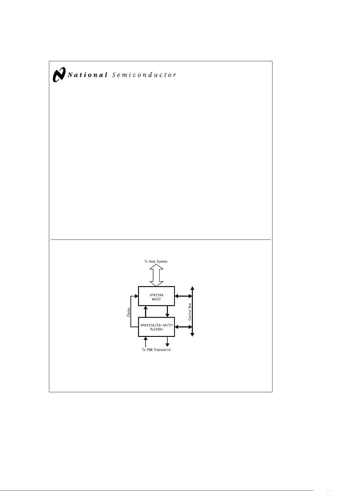
FIGURE 1-1. FDDI Chip Set Overview
TRI-STATEÉis a registered trademark of National Semiconductor Corporation.
BMAC
TM
, BSITM, CDDTM, CDLTM, CRDTM, CYCLONETM, MACSITM, PLAYERTM, PLAYER
a
TM
and TWISTERTMare trademarks of National Semiconductor Corporation.
C
1995 National Semiconductor Corporation RRD-B30M115/Printed in U. S. A.

Table of Contents
1.0 FDDI CHIP SET OVERVIEW
1.1 FDDI 2-Chip Set
1.2 FDDI TP-PMD Solutions
2.0 ARCHITECTURE DESCRIPTION
2.1 Block Overview
2.2 Interfaces
3.0 FUNCTIONAL DESCRIPTION
3.1 Clock Recovery Module
3.2 Receiver Block
3.3 Transmitter Block
3.4 Configuration Switch
3.5 Clock Generation Module
3.6 Station Management Support
3.7 PHY-MAC Interface
3.8 PMD Interface
4.0 MODES OF OPERATION
4.1 Run Mode
4.2 Stop Mode
4.3 Loopback Mode
4.4 Device Reset
4.5 Cascade Mode
5.0 REGISTERS
5.1 Mode Register (MR)
5.2 Configuration Register (CR)
5.3 Interrupt Condition Register (ICR)
5.4 Interrupt Condition Mask Register (ICMR)
5.5 Current Transmit State Register (CTSR)
5.6 Injection Threshold Register (IJTR)
5.7 Injection Symbol Register A (ISRA)
5.8 Injection Symbol Register B (ISRB)
5.9 Current Receive State Register (CRSR)
5.10 Receive Condition Register A (RCRA)
5.11 Receive Condition Register B (RCRB)
5.12 Receive Condition Mask Register A (RCMRA)
5.13 Receive Condition Mask Register B (RCMRB)
5.14 Noise Threshold Register (NTR)
5.15 Noise Prescale Threshold Register (NPTR)
5.16 Current Noise Count Register (CNCR)
5.17 Current Noise Prescale Count Register (CNPCR)
5.18 State Threshold Register (STR)
5.19 State Prescale Threshold Register (SPTR)
5.20 Current State Count Register (CSCR)
5.21 Current State Prescale Count Register (CSPCR)
5.22 Link Error Threshold Register (LETR)
5.23 Current Link Error Count Register (CLECR)
5.24 User Definable Register (UDR)
5.25 Device ID Register (DIR)
5.26 Current Injection Count Register (CIJCR)
5.27 Interrupt Condition Comparison Register (ICCR)
5.28 Current Transmit State Comparison Register
(CTSCR)
5.29 Receive Condition Comparison Register A (RCCRA)
5.30 Receive Condition Comparision Register B (RCCRB)
5.31 Mode Register 2 (MODE2)
5.32 CMT Condition Comparison Register (CMTCCR)
5.33 CMT Condition Register (CMTCR)
5.34 CMT Condition Mask Register (CMTCMR)
5.35 Reserved Registers 22H-23H (RR22H-RR23H)
5.36 Scrub Timer Threshold Register (STTR)
5.37 Scrub Timer Value Register (STVR)
5.38 Trigger Definition Register (TDR)
5.39 Trigger Transition Configuration Register (TTCR)
5.40 Reserved Registers 28H-3AH (RR28H-RR3AH)
5.41 Clock Generation Module Register (CGMREG)
5.42 Alternate PMD Register (APMDREG)
5.43 Gain Register (GAINREG)
5.44 Reserved Registers 3EH-3FH (RR3EH-RR3FH)
6.0 SIGNAL DESCRIPTIONS
6.1 DP83256VF Signal Descriptions
6.2 DP83256VF-AP Signal Descriptions
6.3 DP83257VF Signal Descriptions
7.0 ELECTRICAL CHARACTERISTICS
7.1 Absolute Maximum Ratings
7.2 Recommended Operating Conditions
7.3 DC Electrical Characteristics
7.4 AC Electrical Characteristics
8.0 CONNECTION DIAGRAMS
8.1 DP83256VF Connection Diagram/Pin Descriptions
8.2 DP83256VF-AP Connection Diagram/Pin Descrip-
tions
8.3 DP83257VF Connection Diagram/Pin Descriptions
9.0 PACKAGE INFORMATION
9.1 Land Patterns
9.2 Mechanical Drawings
2

1.0 FDDI Chip Set Overview
National Semiconductor’s next generation FDDI 2-chip set
consists of two components as shown in
Figure 1-1
. The
PLAYER
a
device integrates the features of the DP83231
CRD
TM
Clock Recovery Device, DP83241 CDDTMClock
Distribution Device, and DP83251/55 PLAYER
TM
Physical
Layer Controller. In addition, the PLAYER
a
device contains
enhanced SMT support.
National Semiconductor’s FDDI TP-PMD Solutions consist
of two componentsÐthe DP83222 CYCLONE
TM
Twisted
Pair FDDI Stream Cipher Device and the DP83223A
TWISTER
TM
Twisted Pair FDDI Transceiver Device.
For more information on the other devices of the chip set,
consult the appropriate datasheets and application notes.
1.1 FDDI 2-CHIP SET
DP83256/56-AP/57 PLAYER
a
Device Physical Layer Controller
The PLAYERadevice implements the Physical Layer
(PHY) protocol as defined by the ANSI FDDI PHY X3T9.5
standard.
Features
Y
Single chip FDDI Physical Layer (PHY) solution
Y
Integrated Digital Clock Recovery Module provides enhanced tracking and greater lock acquisition range
Y
Integrated Clock Generation Module provides all necessary clock signals for an FDDI system from an external
12.5 MHz reference
Y
Alternate PMD Interface (DP83256-AP/57) supports
UTP twisted pair FDDI PMDs with no external clock recovery or clock generation functions required
Y
No External Filter Components
Y
Connection Management (CMT) Support (LEM, TNE,
PCÐReact, CFÐReact, Auto Scrubbing)
Y
Full on-chip configuration switch
Y
Low Power CMOS-BIPOLAR design using a single 5V
supply
Y
Full duplex operation with through parity
Y
Separate management interface (Control Bus)
Y
Selectable Parity on PHY-MAC Interface and Control
Bus Interface
Y
Two levels of on-chip loopback
Y
4B/5B encoder/decoder
Y
Framing logic
Y
Elasticity Buffer, Repeat Filter, and Smoother
Y
Line state detector/generator
Y
Supports single attach stations, dual attach stations
and concentrators with no external logic
Y
DP83256/56-AP for SAS/DAS single path stations
Y
P83257 for SAS/DAS single/dual path stations
In addition, the DP83257 contains the additional PHYÐData.request and PHYÐData.indicate ports required for concentrators and dual attach, dual path stations.
DP83266 MACSITMDevice Media
Access Controller and System
Interface
The DP83266 Media Access Controller and System Interface (MACSI) implements the ANSI X3T9.5 Standard Media
Access Control (MAC) protocol for operation in an FDDI
token ring and provides a comprehensive System Interface.
The MACSI device transmits, receives, repeats, and strips
tokens and frames. It produces and consumes optimized
data structures for efficient data transfer. Full duplex architecture with through parity allows diagnostic transmission
and self testing for error isolation in point-to-point connections.
The MACSI device includes the functionality of both the
DP83261 BMAC device and the DP83265 BSI-2 device with
additional enhancements for higher performance and reliability.
Features
Y
Over 9 Kbytes of on-chip FIFO
Y
5 DMA Channels (2 Output and 3 Input)
Y
12.5 MHz to 33 MHz operation
Y
Full duplex operation with through parity
Y
Real-time VOID frame stripping indicator for bridges
Y
On-chip Address bit swapping capability
Y
32-bit wide Address/Data path with byte parity
Y
Programmable transfer burst sizes of 4 or 8 32-bit
words
Y
Receive frame filtering services
Y
Frame-per-Page mode controllable on each DMA
channel
Y
Demultiplexed Addresses supported on ABus
Y
New multicast address matching
Y
ANSI X3T9.5 MAC standard defined ring service options
Y
Supports all FDDI Ring Scheduling Classes (Synchronous, Asynchronous, etc.)
Y
Supports Individual, Group, Short, Long, and External
Addressing.
Y
Generates Beacon, Claim, and Void frames
Y
Extensive ring and station statistics gathering
Y
Extension for MAC level bridging
Y
Enhanced SBus compatibility
Y
Interfaces to DRAMs or directly to system bus
Y
Supports frame Header/Info splitting
Y
Programmable Big or Little Endian alignment
3

DP83222 CYCLONE Twisted Pair
FDDI Stream Cipher Device
General Description
The DP83222 CYCLONE Stream Cipher Scrambler/Descrambler Device is an integrated circuit designed to interface directly with the serial bit streams of a Twisted Pair
FDDI PMD. The DP83222 is designed to be fully compatible
with the National Semiconductor FDDI Chip Sets, including
twisted pair FDDI Transceivers, such as the DP83223A
Twisted Pair Transceiver (TWISTER). The DP83222 requires a 125 MHz Transmit Clock and corresponding Receive Clock for synchronous data scrambling and descrambling. The DP83222 is compliant with the ANSI X3T9.5
TP-PMD standard and is required for the reduction of EMI
emission over unshielded media. The DP83222 is specified
to work in conjunction with existing twisted pair transceiver
signalling schemes and enables high bandwidth transmission over Twisted Pair copper media.
Features
Y
Enables 100 Mbps FDDI signalling over Category 5
Unshielded Twisted Pair (UTP) cable and Type 1
Shielded Twisted Pair (STP)
Y
Reduces EMI emissions over Twisted Pair media
Y
Compatible with ANSI X3T9.5 TP-PMD standard
Y
Requires a singlea5V supply
Y
Transparent mode of operation
Y
Flexible NRZ and NRZI format options
Y
Advanced BiCMOS process
Y
Signal Detect and Clock Detect inputs provided for enhanced functionality
Y
Suitable for Fiber Optic PMD replacement applications
DP83223A TWISTER High Speed
Networking Transceiver Device
General Description
The DP83223A Twisted Pair Transceiver is an integrated
circuit capable of driving and receiving either binary or
(MLT-3) encoded datastreams. The DP83223A Transceiver
is designed to interface directly with standards compliant
FDDI, 100BASE-TX or STS-3c ATM chip sets, allowing low
cost data links over copper based media. The DP83223A
allows links of up to 100 meters over both Shielded Twisted
Pair (STP) and datagrade Unshielded Twisted Pair (UTP) or
equivalent. The electrical performance of the DP83223A
meets or exceeds all performance parameters specified
in the ANSI X3T9.5 TP-PMD standard, the IEEE 802.3
100BASE-TX Fast Ethernet Specification and the ATM Forum 155 Mbps Twisted Pair PMD Interface Specification.
The DP83223A also provides important features such as
baseline restoration, TRI-STATE
É
capable transmit outputs,
and controlled transmit output edge rates (to reduce EMI
radiation) for both binary and MLT-3 modes of operation.
Features
Y
Compliant with ANSI X3T9.5 TP-PMD standard
Y
Compliant with IEEE 802.3 100BASE-TX Ethernet draft
standard
Y
Compliant with ATM Forum 155 Mbps Twisted Pair
Specification
Y
Integrated baseline restoration circuit
Y
Integrated transmitter and receiver with adaptive equalization circuit
Y
Programmable binary or MLT-3 operation
Y
Isolated TX and RX power supplies for minimum noise
coupling
Y
Controlled transmit output edge rates for reduced EMI
Y
TRI-STATE capable current transmit outputs
Y
Loopback feature for board diagnostics
Y
Programmable transmit voltage amplitude
4
2.0 Architecture Description
2.1 BLOCK OVERVIEW
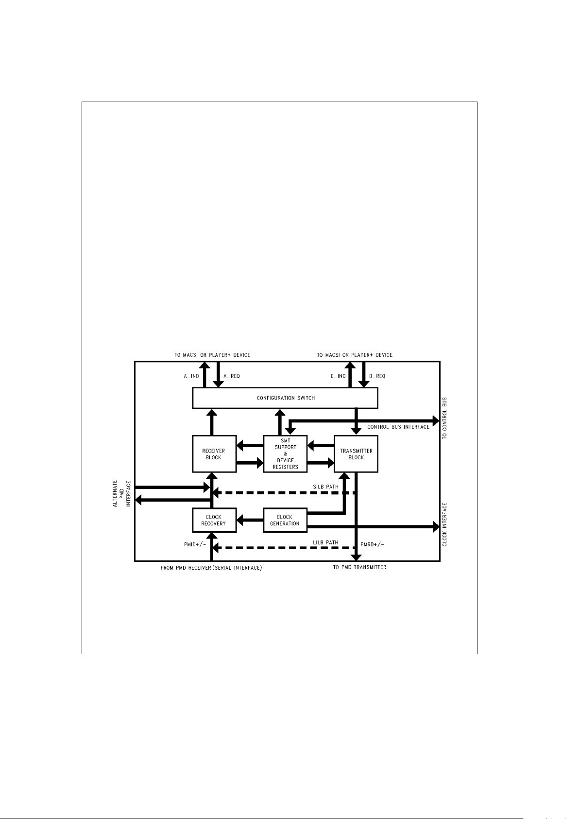
The PLAYERadevice is comprised of six blocks: Clock
Recovery, Receiver, Configuration Switch, Transmitter, Station Management (SMT) Support, and Clock Generation
Module as shown in
Figure 2-1
.
Clock Recovery
The Clock Recovery Module accepts a 125 Mbps NRZI data
stream from the external PMD receiver. It then provides the
extracted and synchronized data and clock to the Receiver
block.
The Clock Recovery Module performs the following operations:
#
Locks to and tracks the incoming NRZI data stream
#
Extracts data stream and synchronized 125 MHz clock
Receiver
During normal operation, the Receiver Block accepts serial
data as inputs at the rate of 125 Mbps from the Clock Recovery Module. During the Internal Loopback mode of operation, the Receiver Block accepts data directly from the
Transmitter Block.
The Receiver Block performs the following operations:
#
Optionally converts the incoming data stream from NRZI
to NRZ.
#
Decodes the data from 5B to 4B coding.
#
Converts the serial bit stream into 10-bit bytes composed
of 8 bits data, 1 bit parity, and 1 bit control information.
#
Compensates for the differences between the upstream
station clock and the local clocks.
#
Decodes Line States.
#
Detects link errors.
#
Presents data symbol pairs (bytes) to the Configuration
Switch Block.
Configuration Switch
An FDDI station may be in one of three configurations: Isolate, Wrap or Thru. The Configuration Switch supports these
configurations by switching the transmitted and received
data paths between PLAYER
a
devices and one or more
MACSI devices.
The configuration switch is integrated into the PLAYER
a
device, therefore no external logic is required for this function.
Setting the Configuration switch can be done explicitly via
the Control Bus Interface or it can be set automatically with
the CFÐReact SMT Support feature.
TL/F/11708– 2
FIGURE 2-1. PLAYERaDevice Block Diagram
5

2.0 Architecture Description (Continued)
Transmitter
The Transmitter Block accepts 10-bit bytes composed of 8
bits data, 1 bit parity, and 1 bit control information from the
Configuration Switch.
The Transmitter Block performs the following operations:
#
Encodes the data from 4B to 5B coding.
#
Filters out code violations from the data stream.
#
Generates Idle, Master, Halt, Quiet, or other user defined
symbol pairs upon request.
#
Converts the data stream from NRZ to NRZI format for
transmission.
#
Provides smoothing function when necessary.
During normal operation, the Transmitter Block presents serial data to the PMD transmitter. While in Internal Loopback
mode, the Transmitter Block presents serial data to the Receiver Block. While in the External Loopback mode, the
Transmitter Block presents serial data to the Clock Recovery Module.
Clock Generation Module
The Clock Generation Module is an integrated phase locked
loop that generates all of the required clock signals for the
PLAYER
a
device and an FDDI system from a single
12.5 MHz reference.
The Clock Generation Module features:
#
High precision clock timing generated from a single
12.5 MHz reference.
#
Multiple precision phased (8 ns/16 ns) 12.5 MHz Local
Byte Clocks to eliminate timing skew in large multi-board
concentrator configurations.
#
LBC timing which is insensitive to loading variations over
a wide range (20 pF to 70 pF) of LBC loads.
#
A selectable dual frequency system clock.
#
Low clock edge jitter, due to high VCO stability.
Station Management (SMT) Support
The Station Management Support Block provides a number
of useful features to simplify the implementation of the Connection Management (CMT) portion of SMT.
These features eliminate the time critical CMT response
time constraints imposed by PCÐReact and CFÐReact
times.
Integrated counters and timers eliminate the need for additional external devices.
The following are the CMT features supported:
#
PCÐReact
#
CFÐReact
#
Auto Scrubbing (TCF Timer)
#
Timer, Idle Detection (TID Timer)
#
Noise Event Counter (TNE Timer)
#
Link Error Monitor (LEM Counter)
2.2 INTERFACES
The PLAYER
a
device connects to other devices via five
functional interfaces: PMD Interface, PHY Port Interface,
Control Bus Interface, Clock Interface, and the Miscellaneous Interface.
PMD Interface
The PMD Interface connects the PLAYER
a
device to a
standard FDDI Physical Media Connection such as a fiber
optic transceiver or a copper twisted pair transceiver. It is a
125 MHz full duplex serial connection.
The DP83256-AP and DP83257 PLAYER
a
devices contain
two PMD interfaces. The Primary PMD Interface should be
used for all PMD implementations that do not require an
external scrambler/descrambler function, clock recovery
function, or clock generation function, such as a Fiber Optic
or Shielded Twisted Pair (SDDI) PMD. The second, Alternate PMD Interface can be used to support Unshielded
Twisted Pair (UTP) PMDs that require external scrambling,
and allows implementation with no external clock recovery
or clock generation functions required.
PHY Port Interface
The PHY Port Interface connects the PLAYER
a
device to
one or more MAC devices and/or PLAYER
a
devices. Each
PHY Port Interface consists of two byte-wide interfaces, one
for PHY Request data input to the PLAYER
a
device and
one for the PHY Indicate data output of the PLAYER
a
device. Each byte-wide interface consists of a parity bit (odd
parity), a control bit, and two 4-bit symbols.
The DP83257 PLAYER
a
device has two PHY Port Interfac-
es while the DP83256 has one PHY Port Interface.
Control Bus Interface
The Control Bus Interface connects the PLAYER
a
device
to a wide variety of microprocessors and microcontrollers.
The Control Bus is an asynchronous interface which provides access to 64 8-bit registers which monitor and control
the behavior of the PLAYER
a
device.
The Control Bus Interface allows a user to:
#
Configure SMT features.
#
Program the Configuration Switch.
#
Enable/disable functions within the Transmitter and Receiver Blocks (i.e., NRZ/NRZI Encoder, Smoother, PHY
Request Data Parity, Line State Generation, Symbol pair
Injection, NRZ/NRZI Decoder, Cascade Mode, etc.).
The Control Bus Interface also can be used to perform the
following functions:
#
Monitor Line States received.
#
Monitor link errors detected by the Receiver Block.
#
Monitor other error conditions.
Clock Interface
The Clock Interface is used to configure the Clock Generation Module and to provide the required clock signals for an
FDDI system.
The following clock signals are generated:
#
5 phase offset 12.5 MHz Local Byte Clocks
#
25 MHz Local Symbol Clock
#
15.625 or 31.25 MHz System Clock
Miscellaneous Interface
The Miscellaneous Interface consists of:
#
A reset signal.
#
User definable sense signals.
#
User definable enable signals.
#
Synchronization for cascading PLAYERadevices (a
high-performance non-FDDI mode).
#
Device Power and Ground pins.
6
3.0 Functional Description
The PLAYERadevice is comprised of six blocks: Clock
Recovery, Receiver, Transmitter, Configuration Switch,
Clock Generation, and Station Management Support.
3.1 CLOCK RECOVERY MODULE
The Clock Recovery Module accepts a 125 Mbps NRZI data
stream from the external PMD receiver. It then provides the
extracted and synchronized data and clock to the Receiver
block.
The Clock Recovery Module performs the following operations:
#
Locks onto and tracks the incoming NRZI data stream
#
Extracts the data stream and the synchronized 125 MHz
clock
The Clock Recovery Module is implemented using an advanced digital architecture that replaces sensitive analog
blocks with digital circuitry. This allows the PLAYER
a
device to be manufactured to tighter tolerances since it is less
sensitive to processing variations that can adversely affect
analog circuits.
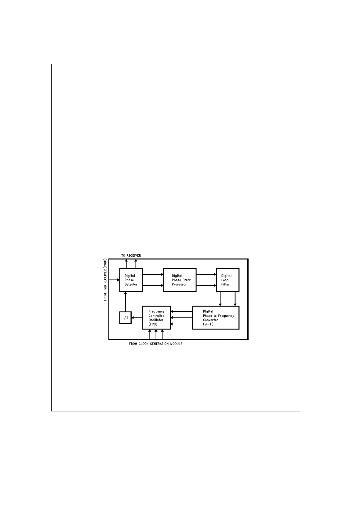
The Clock Recovery Module is comprised of 5 main functional blocks:
Digital Phase Detector
Digital Phase Error Processor
Digital Loop Filter
Digital Phase to Frequency Converter
Frequency Controlled Oscillator
See
Figure 3-1
, Clock Recovery Module Block Diagram.
DIGITAL PHASE DETECTOR
The Digital Phase Detector has two main functions: phase
error detection and data recovery.
Phase error detection is accomplished by a digital circuit
that compares the input data (PMID) to an internal phaselocked 125 MHz reference clock and generates a pair of
error signals. The first signal is a pulse whose width is equal
to the phase error between the input data and a reference
clock and the second signal isa4nsreference pulse.
These signals are fed into the Digital Phase Error Processor
block.
The data recovery function converts the incoming encoded
data stream (PMID) into synchronized data and clock signals. When the circuit is in lock the rising edge of the recovered clock is exactly centered in the recovered data bit cell.
The digital phase detector uses a common path for phase
error detection and data recovery so as to minimize clock
Static Alignment Error (SAE). Phase error averaging is also
included so that phase errors generated by positive and
negative PMID edges equally affect the clock recovery circuit. This greatly improves the immunity to Duty Cycle Distortion (DCD) in the data recovery circuit.
DIGITAL PHASE ERROR PROCESSOR
The Digital Phase Error Processor is responsible for sampling the Phase Detector’s phase error outputs and producing two digital outputs that indicate to the digital loop filter
how to adjust for a difference between the data phase and
reference phases.
The Phase Error Processor is designed to eliminate the effects of different clock edge densities between data symbols and the various line state symbols on the PLL’s loop
gain.
TL/F/11708– 3
FIGURE 3-1. Clock Recovery Module Block Diagram
7

3.0 Functional Description (Continued)
Since the loop gain is held constant regardless of the incoming signal edge density, PLL characteristics such as jitter, acquisition rate, locking range etc., are deterministic and
show minimal spread under various operating environments.
The phase error processor also automatically puts the loop
in open-loop-mode when the incoming data stream contains
abnormal low edge rates. When the PLL is in open-loopmode, no update is made to the PLL’s filter variables in the
filter block. The PLL can then use the pretrained frequency
and phase contents to perform data recovery. Since the
loop is implemented digitally, these values (the frequency
and phase variables) are retained. The resolution of the frequency variable is about 1.3 ppm of the incoming frequency.
The resolution of the phase variable is about 40 ps.
DIGITAL LOOP FILTER
The digital loop filter emulates a 1-pole, 1-zero filter and
uses an automatic acquisition speed control circuit to dynamically adjust loop parameters.
The digital loop filter takes the phase error indicator signals
Data Valid and Up/Down from the Phase Error processor
and accumulates errors over a few cycles before passing on
the Data Valid and Up/Down signals to the Phase Error to
Frequency converter.
The filter has 4 sets of bandwidth and damping parameters
which are switched dynamically by an acquisition control
circuit. The input Signal Detect (SD) starts the sequence
and, thereafter, no user programming is required to finish
the sequence.
At the completion of the locking sequence, the loop has the
narrowest bandwidth such that the loop produces minimal
recovered clock jitter. The PLL can track an incoming frequency offset of approximately
g
200 ppm. After the acquisition sequence, the equivalent natural frequency of the
loop is reduced to about 7 kHz (
g
56 ppm) of frequency
offset.
The automatic tracking mechanism allows the loop to quickly lock onto the initial data stream for data recovery (typically less than 10 ms) and yet produce very little recovered
clock jitter.
PHASE ERROR TO FREQUENCY CONVERTER (O–F)
The Phase Error to Frequency Converter takes the Data
Valid and Up/Down signals modified by the Digital Loop
Filter and converts them to triangle waves. The frequency of
the triangle waves is then used to control the Frequency
Controlled Oscillator’s (FCO) 250 MHz oscillations.
Each valid Up or Down signal causes a partial 7-bit counter
(using only 96 counts) to increment or decrement at the
O
–F converter’s clock rate of 15.625 MHz (250 MHz/16).
When the Data Valid signal is not asserted, the counter
holds count.
The counter value is used to produce 3 triangle waves that
are offset in phase by 120 degrees. This is done with a
special Pulse Density Modulator waveform synthesizer
which takes the place of a traditional Digital-Analog converter. The frequency of the triangle waves tells the Frequency
Controlled Oscillator how much to adjust oscillation. The
phase relationships (leading or lagging) between the 3 signals indicates the direction of change.
The minimum frequency of the triangle waves is 0 and corresponds to the case when the PLL is in perfect lock with
the incoming signal.
The maximum frequency that the
O
–F converter can produce determines the locking range of the PLL. In this case
the maximum frequency of each triangle wave is 162.76
kHz, which is produced when the
O
–F converter gets a
continuous count in one direction that is valid every
O
–F
converter clock cycle of 15.625 MHz (250 MHz/16). The
triangle waves have an amplitude resolution of 48 digital
steps, so a full rising and falling period takes 96 counts
which produces a maximum frequency of 162.76 kHz
(1/(1/15.625 kHz * 96)).
The 96 digital counts of the triangle waves also lead to a
very fine PLL phase resolution of 42 ps (4 ns/96 counts).
This high phase resolution is achieved using very low frequency signals, in contrast to a standard PLL which must
operate at significantly higher frequencies than the data being tracked to achieve such high phase resolution.
FREQUENCY CONTROLLED OSCILLATOR (FCO)
The frequency controlled oscillator produces a 250 MHz
clock that, when divided by 2, is phase locked to the incoming data’s clock.
The FCO uses three 250 MHz reference clock signals from
the Clock Generation Module and three 0 Hz to 162.76 kHz
error clock signals from the Phase Error to Frequency Converter as inputs. Each signal in a triplet is 120 degrees
phase shifted from the next.
Each corresponding pair (one 250 MHz and one error signal) of signals is mixed together using an amplitude switching modulator, with the error signal modulating the reference. All of the outputs are then summed together to produce the final 250 MHz
a
fmphase locked clock signal,
where f
m
is the error frequency.
8
3.0 Functional Description (Continued)
3.2 RECEIVER BLOCK
During normal operation, the Receiver Block accepts serial
data input at the rate of 125 Mbps from the Clock Recovery
Module. During the Internal Loopback mode of operation,
the Receiver Block accepts input data from the Transmitter
Block.
The Receiver Block performs the following operations:
#
Optionally converts the incoming data stream from NRZI
to NRZ.
#
Decodes the data from 5B to 4B coding.
#
Converts the serial bit stream into the National byte-wide
code.
#
Compensates for the differences between the upstream
station clock and the local clock.
#
Decodes Line States.
#
Detects link errors.
#
Presents data symbol pairs to the Configuration Switch
Block.
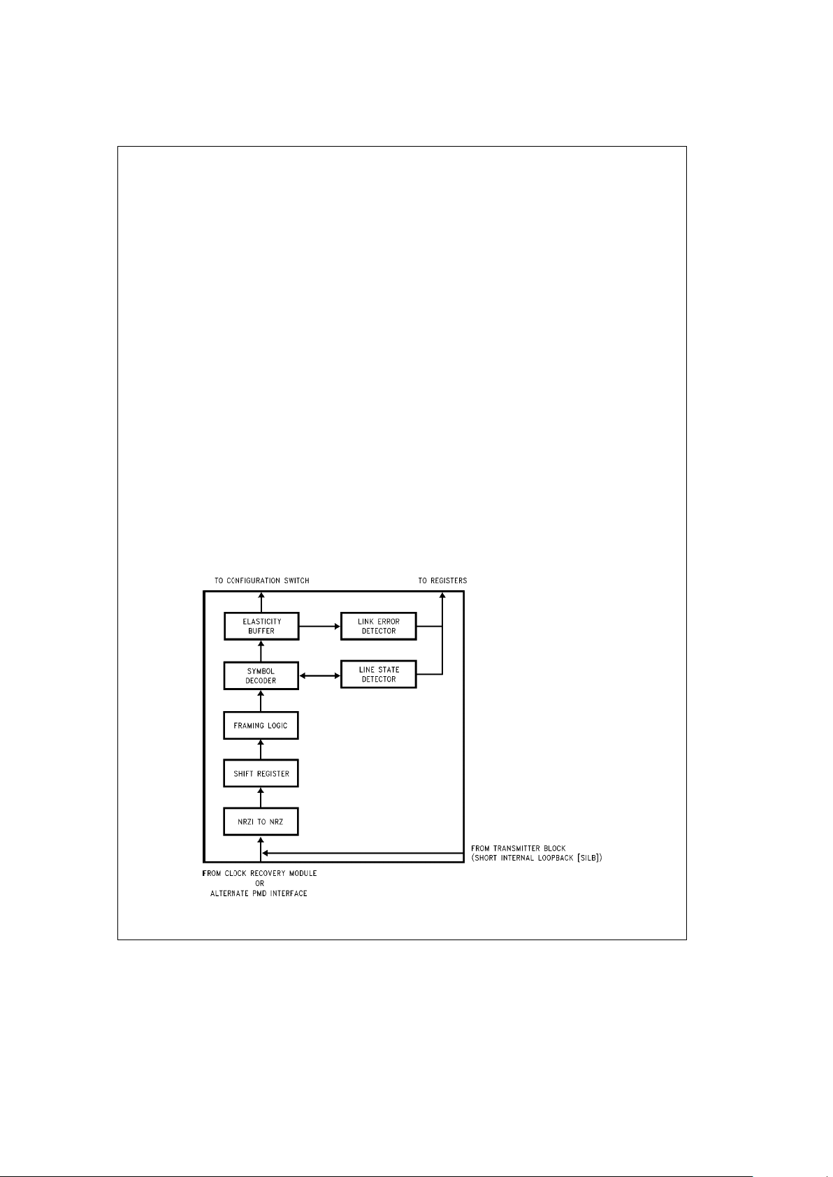
The Receiver Block consists of the following functional
blocks:
NRZI to NRZ Decoder
Shift Register
Framing Logic
Symbol Decoder
Line State Detector
Elasticity Buffer
Link Error Detector
See
Figure 3-2.
NRZI TO NRZ DECODER
The NRZI to NRZ Decoder converts Non-Return-To-ZeroInvert-On-Ones data to Non-Return-To-Zero format.
NRZ format data is the natural data format that the receiver
block utilizes internally, so this function is required when the
standard NRZI format data is fed into the device. The receiver block can bypass this conversion function in the case
where an alternate data source outputs NRZ format data.
This function can be enabled and disabled through bit 7
(RNRZ) of the Mode Register (MR). When the bit is cleared,
it converts the incoming bit stream from NRZI to NRZ. This
is the normal configuration required. When the bit is set, the
incoming NRZ bit stream is passed unchanged.
SHIFT REGISTER
The Shift Register converts the serial bit stream into symbol-wide data for the 5B/4B Decoder.
The Shift Register also provides byte-wide data for the
Framing Logic.
FRAMING LOGIC
The Framing Logic performs the Framing function by detecting the beginning of a frame or the Halt-Halt or Halt-Quiet
symbol pair.
The J-K symbol pair (11000 10001) indicates the beginning
of a frame during normal operation. The Halt-Halt (00100
00100) and Halt-Quiet (00100 00000) symbol pairs are detected for Connection Management (CMT).
TL/F/11708– 4
FIGURE 3-2. Receiver Block Diagram
9
3.0 Functional Description (Continued)
Framing may be temporarily suspended (i.e. framing hold),
in order to maintain data integrity.
Detecting JK
The JK symbol pair can be used to detect the beginning of a
frame during Active Line State (ALS) and Idle Line State
(ILS) conditions.
While the Line State Detector indicates Idle Line State the
receiver ‘‘reframes’’ upon detecting a JK symbol pair and
enters the Active Line State.
During Active Line State, acceptance of a JK symbol (reframing) is allowed for any on-boundary JK which is detected at least 1.5 byte times after the previous JK.
During Active Line State, once reframed on a JK, a subsequent off-boundary JK is ignored, even if it is detected beyond 1.5 byte times after the previous JK.
During Active Line State, an Idle or Ending Delimiter (T)
symbol will allow reframing on any subsequent JK, if a JK is
detected at least 1.5 byte times after the previous JK.
Detecting HALT-HALT AND HALT-QUIET
During Idle Line State, the detection of a Halt-Halt, or HaltQuiet symbol pair will still allow the reframing of any subsequent on-boundary JK.
Once a JK is detected during Active Line State, off-boundary Halt-Halt, or Halt-Quiet symbol pairs are ignored until the
Elasticity Buffer (EB) has an opportunity to recenter. They
are treated as violations.
After recentering on a Halt-Halt, or Halt-Quiet symbol pair,
all off boundary Halt-Halt or Halt-Quiet symbol pairs are ignored until the EB has a chance to recenter during a line
state other than Active Line State (which may be as long as
2.8 byte times).
SYMBOL DECODER
The Symbol Decoder is a two level system. The first level is
a 5-bit to 4-bit converter, and the second level is a 4-bit
symbol pair to byte-wide code converter.
The first level latches the received 5-bit symbols and decodes them into 4-bit symbols. Symbols are decoded into
two types: data and control. The 4-bit symbols are sent to
the Line State Detector and the second level of the Symbol
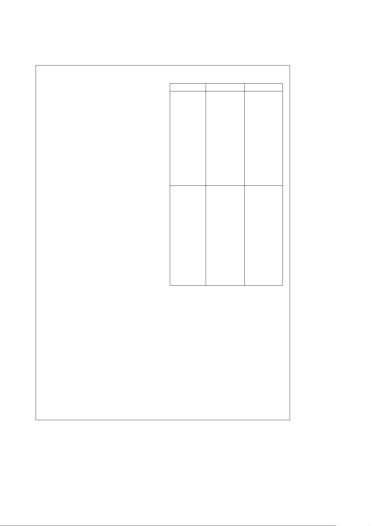
Decoder. See Table 3-1 for the 5B/4B Symbol Decoding
list.
The second level translates two symbols from the 5B/4B
converter and the line state information from the Line State
Detector into the National byte-wide code.
LINE STATE DETECTOR
The ANSI X3T9.5 FDDI Physical Layer (PHY) standard
specifies eight Line States that the Physical Layer can
transmit. These Line States are used in the Connection
Management process. They are also used to indicate data
within a frame during normal operation.
The Line States are reported through the Current Receive
State Register (CRSR), Receive Condition Register A
(RCRA), and Receive Condition Register B (RCRB).
TABLE 3-1. 5B/4B Symbol Decoding
Symbol Incoming 5B Decoded 4B
0 11110 0000
1 01001 0001
2 10100 0010
3 10101 0011
4 01010 0100
5 01011 0101
6 01110 0110
7 01111 0111
8 10010 1000
9 10011 1001
A 10110 1010
B 10111 1011
C 11010 1100
D 11011 1101
E 11100 1110
F 11101 1111
I (Idle) 11111 1010
H (Halt) 00100 0001
JK (Starting 11000 and 1101
Delimiter) 10001
T (Ending 01101 0101
Delimiter)
R (Reset) 00111 0110
S (Set) 11001 0111
Q (Quiet) 00000 0010
V (Violation) 00001 0010
V 00010 0010
V 00011 0010
V 00101 0010
V 00110 0010
V 01000 0010
V 01100 0010
V 10000 0010
Note: VÊdenotes PHY Invalid or an Elasticity Buffer stuff byte
I
Ê
denotes Idle symbol in ILS or an Elasticity Buffer stuff byte
LINE STATES DESCRIPTION
Active Line State
The Line State Detector recognizes the incoming data to be
in the Active Line State upon the reception of the Starting
Delimiter (JK symbol pair).
The Line State Detector continues to indicate Active Line
State while receiving data symbols, Ending Delimiter (T
symbols), and Frame Status symbols (R and S) after the JK
symbol pair.
Idle Line State
The Line State Detector recognizes the incoming data to be
in the Idle Line State upon the reception of 2 Idle symbol
pairs nominally (plus up to 9 bits of 1 in start up cases).
Idle Line State indicates the preamble of a frame or the lack
of frame transmission during normal operation. Idle Line
State is also used in the handshake sequence of the PHY
Connection Management process.
10

3.0 Functional Description (Continued)
Super Idle Line State
The Line State Detector recognizes the incoming data to be
in the Super Idle Line State upon the reception of 8 consecutive Idle symbol pairs nominally (plus 1 symbol pair).
The Super Idle Line State is used to insure synchronization
of PCM signalling.
No Signal Detect
The Line State Detector recognizes the incoming data to be
in the No Signal Detect state upon the deassertion of the
Signal Detect signal or lack of internal clock detect from the
Clock Recovery Module, and reception of 8 Quiet symbol
pairs nominally. No Signal Detect indicates that the incoming link is inactive. This is the same as receiving Quiet Line
State (QLS).
Master Line State
The Line State Detector recognizes the incoming data to be
in the Master Line State upon the reception of eight consecutive Halt-Quiet symbol pairs nominally (plus up to 2 symbol
pairs in start up cases).
The Master Line State is used in the handshaking sequence
of the PHY Connection Management process.
Halt Line State
The Line State Detector recognizes the incoming data to be
in the Halt Line State upon the reception of eight consecutive Halt symbol pairs nominally (plus up to 2 symbol pairs in
start up cases).
The Halt Line State is used in the handshaking sequence of
the PHY Connection Management process.
Quiet Line State
The Line State Detector recognizes the incoming data to be
in the Quiet Line State upon the reception of eight consecutive Quiet symbol pairs nominally (plus up to 9 bits of 0 in
start up cases).
The Quiet Line State is used in the handshaking sequence
of the PHY Connection Management process.
Noise Line State
The Line State Detector recognizes the incoming data to be
in the Noise Line State upon the reception of 16 noise symbol pairs without entering any known line state.
The Noise Line State indicates that data is not being received correctly.
Line State Unknown
The Line State Detector recognizes the incoming data to be
in the Line State Unknown state upon the reception of 1
inconsistent symbol pair (i.e. data that is not expected). This
may signify the beginning of a new line state.
Line State Unknown indicates that data is not being received correctly. If the condition persists the Noise Line
State (NLS) may be entered.
ELASTICITY BUFFER
The Elasticity Buffer performs the function of a ‘‘variable
depth’’ FIFO to compensate for phase and frequency clock
skews between the Receive Clock (RXC
g
) and the Local
Byte Clock (LBC).
Bit 5 (EBOU) of the Receive Condition Register B (RCRB) is
set to 1 to indicate an error condition when the Elasticity
Buffer cannot compensate for the clock skew.
The Elasticity Buffer will support a maximum clock skew of
50 ppm with a maximum packet length of 4500 bytes.
To make up for the accumulation of frequency disparity between the two clocks, the Elasticity Buffer will insert or delete Idle symbol pairs in the preamble. Data is written into
the byte-wide registers of the Elasticity Buffer with the Receive Clock, while data is read from the registers with the
Local Byte Clock.
The Elasticity Buffer will recenter (i.e. set the read and write
pointers to a predetermined distance from each other) upon
the detection of a JK or every four byte times during PHY
Invalid (i.e. MLS, HLS, QLS, NLS, NSD) and Idle Line State.
The Elasticity Buffer is designed such that a given register
cannot be written and read simultaneously under normal operating conditions. To avoid metastability problems, the EB
overflow event is flagged and the data is tagged before the
over/under run actually occurs.
LINK ERROR DETECTOR
The Link Error Detector provides continuous monitoring of
an active link (i.e. during Active and Idle Line States) to
insure that it does not exceed the maximum Bit Error Rate
requirement as set by the ANSI standard for a station to
remain on the ring.
Upon detecting a link error, the internal 8-bit Link Error Monitor Counter is decremented. The start value for the Link
Error Monitor Counter is programmed through the Link Error
Threshold Register (LETR). When the Link Error Monitor
Counter reaches zero, bit 4 (LEMT) of the Interrupt Condition Register (ICR) is set to 1. The current value of the Link
Error Monitor Counter can be read through the Current Link
Error Count Register (CLECR). For higher error rates the
current value is an approximate count because the counter
rolls over.
There are two ways to monitor Link Error Rate: polling and
interrupt.
Polling
The Link Error Monitor Counter can be set to a large value,
like FF. This will allow for the greatest time between polling
the register. This start value is programmed through the Link
Error Threshold Register (LETR).
Upon detecting a link error, the Line Error Monitor Counter
is decremented.
The Host System reads the current value of the Link Error
Monitor Counter via the Current Link Error Count Register
(CLECR). The Counter is then reset to FF.
Interrupt
The Link Error Monitor Counter can be set to a small value,
like 5 to 10. This start value is programmed through the Link
Error Threshold Register (LETR).
Upon detecting a link error, the Line Error Monitor Counter
is decremented. When the counter reaches zero, bit 4
(LEMT) of the Interrupt Condition Register (ICR) is set to 1,
and the interrupt signal goes low, interrupting the Host System.
Miscellaneous Items
When bit 0 (RUN) of the Mode Register (MR) is set to zero,
or when the PLAYER
a
device is reset through the Reset
pin (ERST), the internal signal detect line is internally
forced to zero and the Line State Detector is set to Line
State Unknown and No Signal Detect.
11

3.0 Functional Description (Continued)
3.3 TRANSMITTER BLOCK
The Transmitter Block accepts 10-bit bytes consisting of
8 bits data, 1 bit parity, and 1 bit control information, from
the Configuration Switch.
The Transmitter Block performs the following operations:
#
Encodes the data from 4B to 5B coding.
#
Filters out code violations from the data stream.
#
Is capable of generating Idle, Master, Halt, Quiet, or other user defined symbol pairs.
#
Converts the data stream from NRZ to NRZI for transmission.
#
Serializes data.
During normal operation, the Transmitter Block presents serial data to a PMD transmitter.
While in Internal Loopback mode, the Transmitter Block
presents serial data to the Receiver Block. While in the External Loopback mode, the Transmitter Block presents serial data to the Clock Recovery Module.
The Transmitter Block consists of the following functional
blocks:
Data Registers
Parity Checker
4B/5B Encoder
Repeat Filter
Smoother
Line State Generator
Injection Control Logic
Shift Register
NRZ to NRZI Encoder
See
Figure 3-3
, Transmitter Block Diagram.
TL/F/11708– 5
FIGURE 3-3. Transmitter Block Diagram
12
3.0 Functional Description (Continued)
DATA REGISTERS
Data from the Configuration Switch is stored in the Data
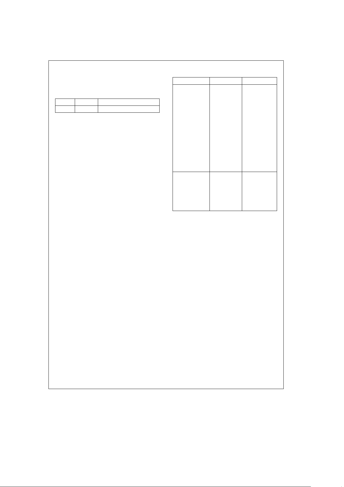
Registers. The 10-bit byte-wide data consists of a parity bit,
a control bit, and two 4-bit data symbols as shown below.
b9 b8 b7 b0
Parity Bit Control Bit Data Bits
FIGURE 3-4. Byte-Wide Data
The parity is odd parity. The control bit determines whether
the Data bits represent Data or Control information. When
the control bit is 0 the Data field is interpreted as data and
when it is 1 the field is interpreted as control information
according to the National Semiconductor control codes.
PARITY CHECKER
The Parity Checker verifies that the parity bit in the Data
Register represents odd parity (i.e. odd number of 1s).
The parity is enabled and disabled through bit 6 (PRDPE) of
the Current Transmit State Register (CTSR).
If a parity error occurs, the Parity Checker will set bit 0 (DPE)
in the Interrupt Condition Register (ICR) and report the error
to the Repeat Filter.
4B/5B ENCODER
The 4B/5B Encoder converts the two 4-bit data symbols
from the Configuration Switch into their respective 5-bit
codes.
See Table 3-2 for the Symbol Encoding list.
TABLE 3-2. 4B/5B Symbol Encoding
Symbol 4B Code 5B Code
0 0000 11110
1 0001 01001
2 0010 10100
3 0011 10101
4 0100 01010
5 0101 01011
6 0110 01110
7 0111 01111
8 1000 10010
9 1001 10011
A 1010 10110
B 1011 10111
C 1100 11010
D 1101 11011
E 1110 11100
F 1111 11101
N 0000 11110 or
11111
JK (Starting 1101 11000 and
Delimiter) 10001
T (Ending 0100 or 01101
Delimiter) 0101
R (Reset) 0110 00111
Note: The upper group of symbols are sent with the Control/Data pin set to
Data, while the bottom grouping of symbols are sent with the Control/Data
pin set to Control.
REPEAT FILTER
The Repeat Filter is used to prevent the propagation of
code violations to the downstream station.
Upon receiving violations in data frames, the Repeat Filter
replaces them with two Halt symbol pairs followed by Idle
symbols. Thus the code violations are isolated and recovered at each link and will not be propagated throughout the
entire ring.
13
3.0 Functional Description (Continued)
TL/F/11708– 6
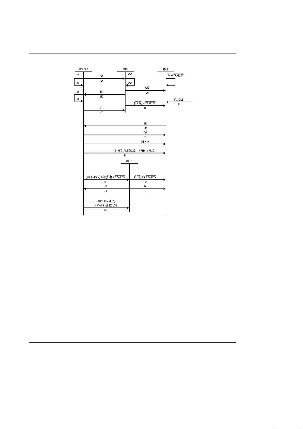
FIGURE 3-5. Repeat Filter State Diagram
Note: Inputs to the Repeat Filter state machine are shown above the transition lines, while outputs from the state machine are shown below the transition lines.
Note: Abbreviations used in the Repeat Filter State Diagram are shown in Table 3-3.
14

3.0 Functional Description (Continued)
TABLE 3-3. Abbreviations used in the
Repeat Filter State Diagram
FÐIDLE: Force IdleÐtrue when not in Active
Transmit Mode.
W: Represents the symbols R, or S, or T
E
TPARITY: Parity error
nn : Data symbols (for C
e
0 in the PHY-MAC
interface)
N: Data portion of a control and data symbol
mixture
X: Any symbol (i.e. don’t care)
V
Ê
: Violation symbols or symbols inserted by
the Receiver Block
I
Ê
: Idle symbols or symbols inserted by the
Receiver Block
ALSZILSZ: Active Line State or Idle Line State (i.e.
PHY Invalid)
E
ALSZILSZ: Not in Active Line State nor in Idle Line
State (i.e. PHY Valid)
H: Halt Symbol
R: Reset Symbol
S: Set Symbol
T: Frame ending delimiter
JK: Frame start delimiter
I: Idle symbol (Preamble)
V: Code violations
The Repeat Filter complies with the FDDI standard by observing the following (see
Figure 3-5
):
1. In Repeat State, violations cause transitions to Halt State
and two Halt symbol pairs are transmitted (unless JK or Ix
occurs) followed by transition to Idle State.
2. When Ix is encountered, the Repeat Filter goes to the Idle
State, during which Idle symbol pairs are transmitted until
a JK is encountered.
3. The Repeat Filter goes to the Repeat State following a JK
from any state.
The END State, which is not part of the FDDI PHY standard,
allows an R or S prior to a T within a frame to be recognized
as a violation. It also allows NT to end a frame as opposed
to being treated as a violation.
SMOOTHER
The Smoother is used to keep the preamble length of a
frame to a minimum of 6 Idle symbol pairs.
Idle symbols in the preamble of a frame may have been
added or deleted by each station to compensate for the
difference between the Receive Clock and its Local Clock.
The preamble needs to be maintained at a minimum length
to allow stations enough time to complete processing of one
frame and prepare to receive another. Without the Smoother function, the minimum preamble length (6 Idle symbol
pairs) cannot be maintained as several stations may consecutively delete Idle symbols.
The Smoother attempts to keep the number of Idle symbol
pairs in the preamble at 7 by:
#
Deleting an Idle symbol pair in preambles which have
more than 7 Idle symbol pairs
and/or
#
Inserting an idle symbol pair in preambles which have
less than 7 idle symbol pairs (i.e. Extend State).
The Smoother Counter starts counting upon detecting an
Idle symbol pair. It stops counting upon detecting a JK symbol pair.
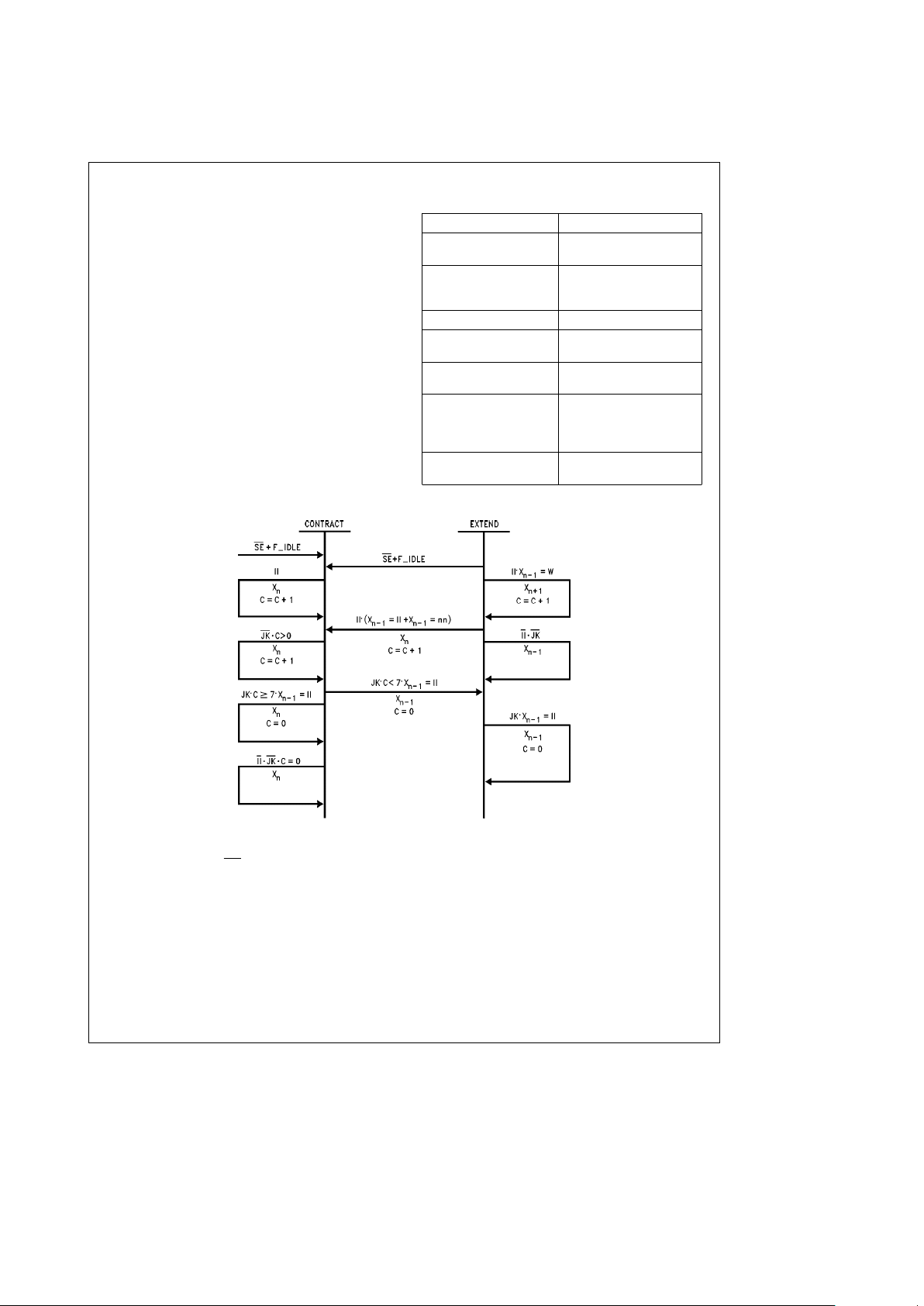
Figure 3-6
describes the Smoother state diagram.
15
3.0 Functional Description (Continued)
LINE STATE GENERATOR
The Line State Generator allows the transmission of the
PHY Request data and can also generate and transmit Idle,
Master, Halt, or Quiet symbol pairs which can be used to
implement the Connection Management procedures as
specified in the FDDI Station Management (SMT) standard
document.
The Line State Generator is programmed through Transmit
bits 0 to 2 (TM
k
2:0l) of the Current Transmit State Regis-
ter (CTSR).
Based on the setting of these bits, the Transmitter Block
operates in a Transmit Mode where the Line State Generator overwrites the Repeat Filter and Smoother outputs.
See INJECTION CONTROL LOGIC section for a listing of
the injection Transmit Modes.
Table 3-4 describes the Transmit Modes.
TABLE 3-4. Transmit Modes
Transit Mode Behavior
Active Transmit Mode Transmit data that comes
from Configuration Switch
Off Transmit Mode Transmit Quiet symbol
pairs and disable the PMD
Transmitter
Idle Transmit Mode Transmit Idle symbol pairs
Master Transmit Mode Transmit Halt-Quiet
symbol pairs
Quiet Transmit Mode Transmit Quiet symbol
pairs
Reserved Transmit Mode Reserved for future use. If
Mode selected, Quiet
symbol pairs will be
transmitted.
Halt Transmit Mode Transmit Halt Symbol
pairs
Notes: TL/F/11708– 7
SE: Smoother Enable
C: Preamble Counter
FÐIDLE: ForceÐIdle (Stop or ATM
)
X
n
: Current Byte
X
n–1
: Previous Byte
W: RST
FIGURE 3-6. Smoother State Diagram
16
3.0 Functional Description (Continued)
INJECTION CONTROL LOGIC
The Injection Control Logic replaces the data stream with a
programmable symbol pair. This function is used to transmit
data other than the normal data frame or Line States. The
injection modes can be used for station diagnostic software.
The Injection Symbols overwrite the Line State Generator
(Transmit Modes) and the Repeat Filter and Smoother outputs.
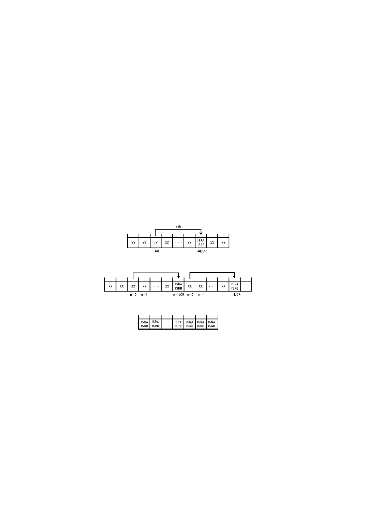
These programmable symbol pairs are stored in the Injection Symbol Register A (ISRA) and Injection Symbol Register B (ISRB). The Injection Threshold Register (IJTR) determines where the Injection Symbol pair will replace the data
symbols.
The Injection Control Logic is programmed through the bits
0 and 1 (IC
k
1:0l) of the Current Transmit State Register
(CTSR) to one of the following Injection Modes (see
Figure
3-7
):
1. No Injection (i.e. normal operation)
2. One Shot
3. Periodic
4. Continuous
In the No Injection mode, the data stream is transmitted
unchanged.
In the One Shot mode, ISRA and ISRB are injected once on
the nth byte after a JK, where n is the programmed value
specified in the Injection Threshold Register.
In the Periodic mode, ISRA and ISRB are injected every nth
symbol.
In the Continuous mode, all data symbols are replaced with
the content of ISRA and ISRB. This is the same as periodic
mode with IJTR
e
0.
SHIFT REGISTER
The Shift Register converts encoded parallel data to serial
data. The parallel data is clocked into the Shift Register by
the Local Byte Clock (LBC1), and clocked out by the Transmit Bit Clock (TXC
g
) (externally available on the DP83257.)
NRZ TO NRZI ENCODER
The NRZ to NRZI Encoder converts the serial Non-ReturnTo-Zero data to Non-Return-To-Zero-Invert-On-One format.
This function can be enabled and disabled through bit 6
(TNRZ) of the Mode Register (MR). When programmed to
‘‘0’’, it converts the bit stream from NRZ to NRZI. When
programmed to ‘‘1’’, the bit stream is transmitted NRZ.
One Shot (Notes 1,3)
TL/F/11708– 8
Periodic (Notes 2,3)
TL/F/11708– 9
Continuous (Note 3)
TL/F/11708– 10
Note 1: In one shot, when ne0, the JK is replaced
Note 2: In periodic, when n
e
0, all symbols are replaced.
Note 3: Max value on n
e
255.
FIGURE 3-7. Injection Modes
17
3.0 Functional Description (Continued)
3.4 CONFIGURATION SWITCH
The Configuration Switch consists of a set of multiplexers
and latches which allow the PLAYER
a
device to configure
the data paths without any external logic. The Configuration
Switch is controlled through the Configuration Register
(CR).
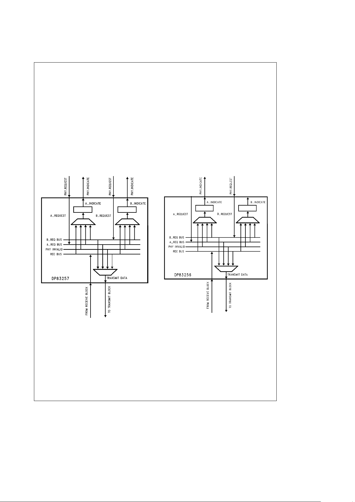
The Configuration Switch has four internal buses: the
AÐRequest bus, the BÐRequest bus, the Receive bus, and
the PHYÐInvalid bus. The two Request buses can be driven by external input data connected to the external PHY
Port interface. The Receive bus is internally connected to
the Receive Block of the PLAYER
a
device, while the
PHYÐInvalid bus has a fixed 10-bit SMT PHY Invalid connection (LSU) pattern (1 0011 1010), which is useful during
the connection process.
The configuration switch also has three internal multiplexers, each can select any of the four buses to connect to its
respective data path. The first two are PHY Port interface
output data paths, AÐIndicate and BÐIndicate, that can
drive output data paths of the external PHY Port interface.
The third output data path is connected internally to the
Transmit Block.
The Configuration Switch is the same on the DP83256 device, the DP83256-AP device, and the DP83257 device.
However, the DP83257 has two PHY Port interfaces connected to the Configuration Switch, whereas the DP83256
and DP83256-AP have one set of PHY port interfaces. The
DP83257 uses the AÐRequest and AÐIndicate paths as
one PHY Port interface and the BÐRequest and BÐIndicate paths as the other PHY Port interface (See
Figure 3-8
).
The DP83256 and DP83256-AP, having one port interface,
use the BÐRequest and AÐIndicate paths as its external
port. The AÐRequest and BÐIndicate paths of the
DP83256 and DP83256-AP are null connections and are not
used by the device (See
Figure 3-9
).
TL/F/11708– 11
FIGURE 3-8. Configuration Switch
Block Diagram for DP83257
TL/F/11708– 12
FIGURE 3-9. Configuration Switch
Block Diagram for DP83256
and DP83256-AP
18
3.0 Functional Description (Continued)
STATION CONFIGURATIONS
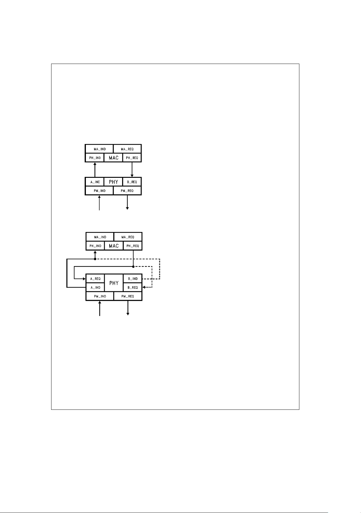
Single Attach Station (SAS)
The Single Attach Station can be connected to either the
Primary or Secondary ring via a Concentrator. Only 1 MAC
is needed in a SAS.
The DP83256, DP83256-AP, and DP83257 can be used in a
Single Attach Station. The DP83256 and DP83256-AP can
be connected to the MAC via its only PHY Port interface.
The DP83257 can be connected to the MAC via either one
of its 2 PHY Port Interfaces.
See
Figure 3-10
and
Figure 3-11
.
TL/F/11708– 13
FIGURE 3-10. Single Attach Station
Using the DP83256 or DP83256-AP
TL/F/11708– 14
FIGURE 3-11. Single Attachment Station (SAS)
Using the DP83257
Dual Attach Station(DAS)
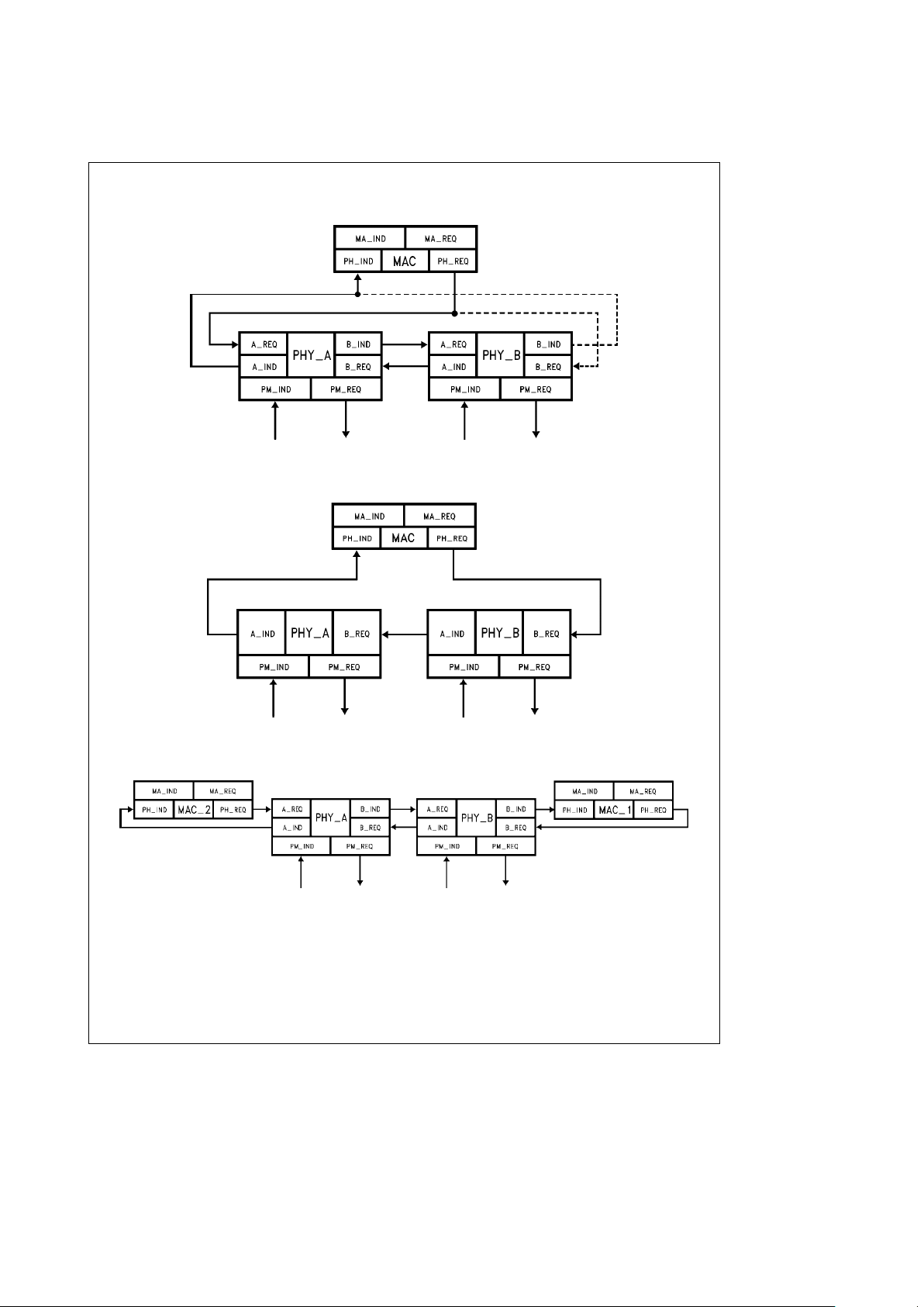
A Dual Attach Station can be connected directly to the dual
ring, or, optionally to a concentrator. There are two types of
Dual Attach Stations: DAS with a single MAC and DAS with
two MAC layers. See
Figure 3-12
and
Figure 3-13
.
Two DP83256 or DP83256-AP parts can be connected together to build a Dual Attach Station, however this configuration does not support the optional ThruÐB configuration.
When the optional ThruÐB configuration is desired, it is recommended that the DP83257 be used.
A DAS with a single MAC and two paths can be configured
as follows (see
Figure 3-12
):
#
B Indicate data of PHYÐA is connected to A Request
input of PHYÐB. BÐRequest input of PHYÐA is connected to A Indicate output of PHYÐB.
#
The MAC can be connected to either the A Request input and the A Indicate output of PHYÐAortheBRequest input and the B Indicate output of PHYÐB.
A DAS with a single MAC and one path using the DP83256
or DP83256-AP can be configured as follows (see
Figure 3-
13
):
#
BÐRequest input of PHYÐA is connected to A Indicate
output of PHYÐB.
#
The MAC is connected to the B Request input of
PHYÐB and the AÐIndicate output of PHYÐA.
A DAS with dual MACs can be configured as follows (see
Figure 3-14
):
#
B Indicate data of PHYÐA is connected to A Request
input of PHYÐB. BÐRequest input of PHYÐA is connected to A Indicate output of PHYÐB.
#
MACÐ1 is connected to the BÐIndicate output and the
BÐRequest Input of PHYÐB.
#
MACÐ2 is connected to the AÐIndicate output and the
AÐRequest Input of PHYÐA.
19
3.0 Functional Description (Continued)
TL/F/11708– 15
FIGURE 3-12. Dual Attachment Station (DAS), Single MAC (DP83257)
TL/F/11708– 16
FIGURE 3-13. Dual Attachment Station (DAS), Single MAC (DP83256/56-AP)
TL/F/11708– 17
FIGURE 3-14. Dual Attachment Station (DAS), Dual MACs
20

3.0 Functional Description (Continued)
CONCENTRATOR CONFIGURATIONS
There are 2 types of concentrators: Single Attach and Dual
Attach. These concentrators can be designed with or without MAC(s). The configuration is determined based upon its
type and the number of active MACs in the concentrator.
Using the PLAYER
a
device, a concentrator can be built
with many different configurations without any external logic.
The DP83256, DP83256-AP, and DP83257 can be used to
build a Single Attach concentrator.
See Application Note AN-675, Designing FDDI concentrators and Application Note AN-741, Differentiating FDDI concentrators for further information.
Concepts
A concentrator is comprised of 2 parts: the Dual Ring Connect portion and the Master Ports.
The Dual Ring Connection portion connects the concentrator to the dual ring directly or to another concentrator. If the
concentrator is connected directly to the dual ring, it is a
part of the ‘‘Dual Ring of Trees’’. If the concentrator is connected to another concentrator, it is a ‘‘Branch’’ of the
‘‘Dual Ring of Trees’’.
The Master Ports connect the concentrator to its ‘‘Slaves’’,
or S-class, Single Attach connections. A slave could be a
Single Attach Station or another concentrator (thus forming
another Branch of the Dual Ring Tree).
When a MAC in a concentrator is connected to the primary
or secondary ring, it is required to be situated at the exit port
of that ring (i.e. its PHÐIND is connected to the IND Interface of the last Master Port in the concentrator (PHYÐMn)
that is connected to that ring).
A concentrator can have two MACs, one connected to the
primary ring and one to the secondary ring. In addition, roving MACs can be included in the concentrator configuration.
A roving MAC can be used to test the stations connected to
the concentrator before allowing them to join the dual ring.
This may require external multiplexers, if used in conjunction with two other MAC layers.
Single Attach Concentrator
A Single Attach concentrator is a concentrator that has only
one PHY at the dual ring connect side. It cannot, therefore,
be connected directly to the dual ring. A Single Attach concentrator is a branch to the dual ring tree. It is connected to
the ring as a slave of another concentrator.
Multiple Single Attach concentrators can be connected together hierarchically to build a multiple levels of branches in
a dual ring.
The Single Attach concentrator can be connected to either
the primary or secondary ring depending on the connection
with its concentrator (the concentrator that it is connected
to as a slave).
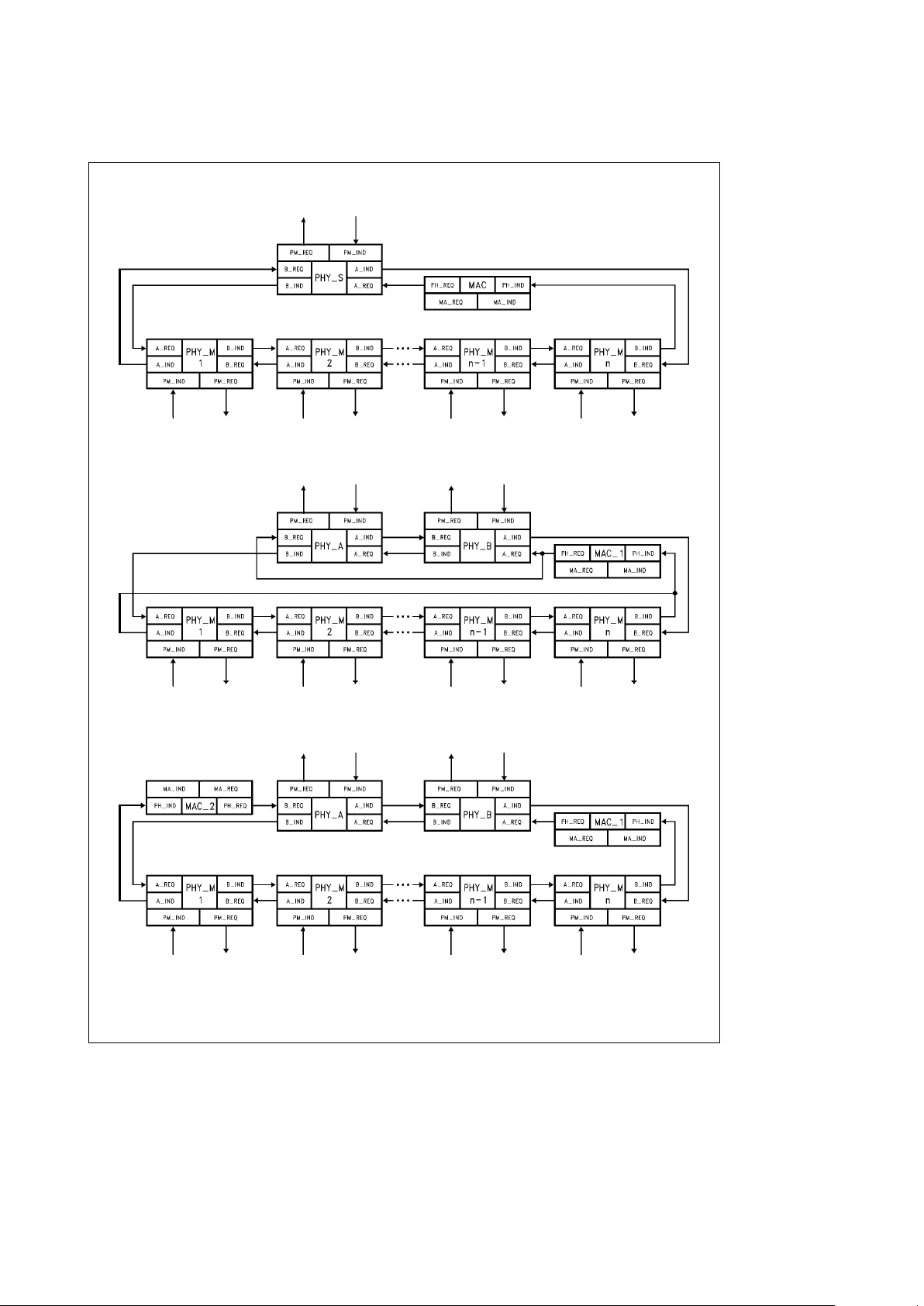
Figure 3-15
shows a Single Attach concentrator with a sin-
gle MAC.
Dual Attach Concentrator
A Dual Attach concentrator is a concentrator that has two
PHYs on the dual ring connect side. It is connected directly
to the dual ring and is a part of the dual ring tree.
The Dual Attach concentrator is connected to both the primary and secondary rings.
Dual Attach Concentrator with Single MAC
Figure 3-16
shows a Dual Attach concentrator with a single
MAC.
Because the concentrator has one MAC, it can only transmit
and receive frames on the ring to which the MAC is connected. The concentrator can only repeat frames on the
other ring.
Dual Attach Concentrator with Dual MACs
Figure 3-17
shows a Dual Attach concentrator with dual
MACs.
Because the concentrator has two MACs, it can transmit
and receive frames on both the primary and secondary
rings.
21
3.0 Functional Description (Continued)
TL/F/11708– 18
FIGURE 3-15. Single Attach Concentrator (SAC), Single MAC
TL/F/11708– 19
FIGURE 3-16. Dual Attach Concentrator (DAC), Single MAC
TL/F/11708– 20
FIGURE 3-17. Dual Attach Concentrator (DAC), Dual MACs
22

3.0 Functional Description (Continued)
3.5 CLOCK GENERATION MODULE
The Clock Generation Module is an integrated phase locked
loop that generates all of the required clock signals for the
PLAYER
a
device and the rest of an FDDI system from a
single 12.5 MHz reference.
The Clock Generation Module features:
#
High precision clock timing generated from a single
12.5 MHz reference.
#
Multiple precision phased (8 ns/16 ns) 12.5 MHz Local
Byte Clocks to eliminate timing skew in large multi-board
concentrator configurations.
#
LBC timing which is insensitive to loading variations over
a wide range (20 pF to 70 pF) of LBC loads.
#
A selectable dual frequency system clock.
#
Low clock edge jitter, due to high VCO stability.
The Clock Generation Module is comprised of 6 main functional blocks:
Reference Selector
Phase Comparator
Loop Filter
250 MHz Voltage Controlled Oscillator
Output Phasing and Divide by 10
See
Figure 3-18
, Clock Generation Module Block Diagram.
REFERENCE SELECTOR
The Reference Selector block allows the user to choose
between 2 sources for the Clock Generation Module’s
12.5 MHz reference clock.
The simplest reference clock source option is to use an
external 12.5 MHz reference signal fed into the REFÐIN
input. This input can come from a crystal oscillator module
or from a Local Byte Clock generated by another PLAYER
a
device. Using the appropriate crystal oscillator ensures correct operating frequency without having to adjust any discrete components.
Using an LBC clock from another PLAYER
a
device allows
one PLAYER
a
device to create a master clock to which
other PLAYER
a
devices in a system can be synchronized.
Another reference clock source option is a local 12.5 MHz
crystal circuit. An example crystal circuit with component
values is shown in
Figure 3-19.
This circuit is designed to
operate with a crystal that has a C
L
of 15 pF. The capacitor
values may need to be slightly adjusted for an individual
application to accomodate differences in parasitic loading.
The REFÐSEL signal selects between the two references.
Component Values
Crystal: 12.50000 MHz
R: 270X 5%
C
ISO
: 56 pF (1%)
C
IN
: 54 pF (1%)
C
OUT
: 54 pF (1%)
TL/F/11708– 22
FIGURE 3-19. Crystal Circuit
PHASE COMPARATOR
The Phase Comparator uses two signal inputs: the selected
12.5 MHz reference from the Reference Select Block and a
Local Byte Clock that has been selected for the feedback
input, FBKÐIN. Typically, LBC1 is used as the feedback
clock.
The Phase Comparator generates a pulse of current that is
proportional to the phase difference between the two signals. The current pulses are used to charge and discharge a
control voltage on the internal Loop Filter. This control voltage is used to minimize the phase difference between the
two signals.
LOOP FILTER
The Loop Filter is a simple internal filter made up of one
capacitor in parallel with a serial capacitor and resistor combination. One end of the filter is connected to Ground and
the other node is driven by the Phase Comparator and controls the internal 250 MHz Voltage Controlled Oscillator.
This node can be examined for diagnostic purposes on the
LPFLTR pin when the FLTREN bit of the CGMREG register
is enabled. The LPFLTR pin is provided for diagnostic purposes only and should not be connected in any application.
TL/F/11708– 21
FIGURE 3-18. Clock Generation Module Block Diagram
23

3.0 Functional Description (Continued)
The voltage on the Loop Filter is set by the current pulses
generated by the Phase Comparator. The voltage on the
Loop Filter node controls the frequency of the 250 MHz
VCO.
250 MHZ VOLTAGE CONTROLLED OSCILLATOR (VCO)
The internal Voltage Controlled Oscillator is a low gain VCO
whose primary frequency of oscillation centers around
250 MHz. The VCO produces little clock jitter due to its
exceptional stability under all circumstances.
The VCO’s output frequency is proportional to the voltage
on the Loop Filter node.
OUTPUT PHASING
The Output Phasing block is a precision clock division circuit
that produces clock signals of 4 distinct frequencies. Within
the 12.5 MHz frequency, 5 clock signals with selectable 8 ns
or 16 ns phase difference are produced.
The following clock signals are produced:
System Clock (CLK16/CLK32)
Local Symbol Clock (LSC)
Local Byte Clocks 1 –5 (LBCn) (Divide by 10)
System Clock (CLK16/CLK32)
The System Clock is provided as an extra set of clock frequencies that may be used as a clock for non-FDDI chipset
portions of a system or as a higher frequency System Interface clock for the MACSI device. This clock is derived by
dividing the 125 MHz clock by 8 or 4 times.
The frequency is selectable through the CLKSEL bit of the
MODE2 register. The output has built-in glitch suppression
so that changing the CLKSEL bit will not result in glitches
appearing at the output.
Local Symbol Clock (LSC)
The Local Symbol Clock is a 40% HIGH/60% LOW duty
cycle clock provided for use by the MACSI device and any
external logic that needs to be synchronized to the Symbol
timing.
This clock is derived by dividing the 125 MHz clock by 5.
Local Byte Clocks 1 –5 (LBCn)
The Local Byte Clocks are provided for use by the MACSI
device, by any external logic that needs to be synchronized
to the Byte timing, and for use in concentrators to synchronize the timing between multiple PLAYER
a
devices.
These clocks are derived by dividing the 125 MHz clock by
10. The different phase relationships between the LBCs are
achieved by tapping off of different outputs of a Johnson
counter inside the Output Phasing block.
The phase relationship (separation by 8 ns or 16 ns) of the
LBCs is selected using the PHÐSEL pin.
One of the LBCs must be used as the source of the feedback input, FBKÐIN, which requires a 12.5 MHz frequency.
When the PLAYER
a
device is using a crystal as a reference it does not matter which LBC is used as the feedback
input. Typically the least loaded LBC is used. However,
when using an external reference that is supplied by another PLAYER
a
device, it is important to select the LBC that
keeps your system properly synchronized. Typically, all devices will use LBC1 as the feedback input.
3.6 STATION MANAGEMENT SUPPORT
The Station Management Support Block provides a number
of useful features to simplify the implementation of the Connection Management (CMT) portion of SMT.
These features eliminate the most severe CMT response
time constraints imposed by the PCÐReact and CFÐReact
times. The many integrated counters and timers also eliminate the need for additional external devices.
The following CMT features are supported:
#
PCÐReact
#
CFÐReact
#
Auto Scrubbing (TCF Timer)
#
Timer, Idle Detection (TID Timer)
#
Noise Event Counter (TNE Timer)
#
Link Error Monitor (LEM Counter)
PCÐREACT
PCÐReact is one of the timing restrictions imposed by Connection Management (CMT). It is one of the two most critical timing restrictions imposed (the other being CFÐReact.)
The ANSI SMT standard states that ‘‘PCÐReact is the maximum time for PCM[Physical Connection Management]to
make a state transition to PCÐBreak when QLS, a fault
condition, or PCÐStart signal is present. This maximum
time also places a limit on the time to react to a PCÐStop
signal. This limitation does not apply to any other PCM transitions.’’ PCÐReact puts a sharp time limit on how long it
takes to transition to the PCÐBreak state and transmit the
correct line state when a PCÐBreak transition is required.
The range for the timer is PCÐReact
s
3.0 ms and has a
default value equal to 3.0 ms.
The PLAYER
a
device contains a Trigger Definition Register and a set of CMT Condition Registers that can be used
to satisfy the PCÐReact timing.
The Trigger Definition Register (TDR) controls two functions. First, it allows the selection of the line state(s) on
which to trigger (SILS, MLS, HLS . . . ). For PCÐReact, the
line states used would be the ones that caused a transition
to the PCÐBreak state from the current PCM state.
Second, it allows specification of a line state to be transmitted when the trigger condition is met. For PCÐReact, this is
the line state that needs to be transmitted when a transition
to the PCÐBreak state occurs, which is Quiet Line State
(QLS).
The set of CMT Condition registers controls interrupt generation when a trigger condition occurs. The CMT Condition
Register set includes a CMT Condition Register (CMTCR), a
CMT Condition Comparison Register (CMTCCR), and a
CMT Condition Mask Register (CMTCMR).
Line state triggering for PCÐReact is enabled by selecting
line states to trigger on from the Trigger Definition Register
(TDR) bits 3-7.
The Trigger Condition Occurred (TCO) bit of the CMTCR is
automatically set when the trigger condition specified by the
TDR register is met.
The line state specified by the Trigger Definition Register
(TDR) bits 0 – 2 is then loaded into the Current Transmit
Mode Register (CTSR), causing the line state to be transmitted.
24

3.0 Functional Description (Continued)
If the TCO Mask (TCOM) bit of the CMTCMR is set, then
whenever the CMTCR.TCO bit becomes set the Receive
Condition Register B’s Connection Service Event
(RCRB.CSE) bit will be set. This allows an interrupt to be
generated for the trigger event.
As an example, suppose the PCM state machine is in the
ACTIVE state. From this state, if a Halt Line State (HLS) or
Quiet Line State (QLS) is detected, or the Noise Threshold
is reached, the state machine must move to the PCÐBreak
state and begin transmitting QLS. To implement this behavior when the PCÐACTIVE state is entered, set
TDR.TTM2–0 to 110 (Quiet Transmit), set TDR.TOHLS,
TDR.TOQLS, and TDR.TONT and reset all other bits (TOSILS and TOMLS). Also set CMTCMR.TCOM if an interrupt
is desired.
CFÐREACT
CFÐReact is one of the timing restrictions imposed by Connection Management (CMT). It is one of the two most critical timing restrictions imposed (the other being
PCÐReact).
The ANSI SMT standard states that ‘‘CFÐReact is the maximum time for CFM[Configuration Management]to reconfigure to remove a non-Active connection from the token
path.’’
The range for the timer is CFÐReact
s
3.0 ms and has a
default value equal to 3.0 ms.
The PLAYER
a
device contains a Trigger Transition Configuration Register and a set of CMT Condition Registers that
can be used to satisfy the CFÐReact timing.
he Trigger Transition Configuration Register (TTCR) holds
the new configuration switch settings to be loaded into the
Configuration Register (CR) when a trigger condition occurs.
Enabling line state triggering with the Trigger Definition Register (TDR) bits 3 – 7 also enables the CFÐReact response.
This means that whenever trigger conditions are actively
used for PCÐReact, the value of the TTCR register will be
used also. This implies that it either must always then be
loaded with the current configuration setting, causing no
change to the CR, or it must be loaded with the appropriate
value to accommodate the CFÐReact function.
The Trigger Transition Configuration Register (TTCR) must
be set the configuration desired when the trigger condition
occurs. When the trigger condition occurs the value of this
register is loaded into the Configuration Register (CR). During this time writes to the CR are inhibited.
To continue the example from the PCÐReact description,
suppose that when in the ACTIVE state for the PCM state
machine, the CFM state machine is also in the THRUÐA
state. If trigger conditions are enabled via the
CMTCMR.TCOM bit and it is desired to not implement CF
Ð
React, TTCR must be set to the present value of CR. If it is
desired to not implement CFÐReact then TTCR should be
set to the value which would change the configuration to the
WRAP state. The wrap conditions WRAPÐA or WRAPÐB
depend on which PHY gets reconfigured.
AUTO SCRUBBING
Auto Scrubbing is an additional CMT feature that further
enhances the automatic configuration switch setting in order to meet the CFÐReact timing. When enabled, Auto
Scrubbing causes 2 PHYÐInvalid symbols followed by
Scrub Symbol pairs (Idles) to be sourced for a user selectable duration (the scrubbing time) after a trigger condition
(the same one used for PCÐReact and CFÐReact) occurs
and prior to a change in the configuration switch setting on
all indicate ports that will be changed.
Auto Scrubbing is enabled by setting the Enable Scrubbing
on Trigger Conditions (ESTC) bit of Mode Register 2
(MODE2).
The Scrub Timer Threshold Register (STTR) defines the duration of the scrubbing, which can last up to approximately
10ms. The Scrub Timer Value Register (STVR) can be used
to examine a snapshot of the upper 8 bits of the STTR
register.
TIMER, IDLE DETECTION
The Idle Detection Timer is required to flag the continued
presence of the Idle Line State for a duration of 8 Idle Symbol pairs plus 1 symbol pair.
This feature is implemented in the Receiver Block by the
Super Idle Line State (SILS).
NOISE EVENT COUNTER
The Noise Event Counter can be used to time the duration
between Noise Events (which are described in detail below)
and to count frame sizes. The first feature is the most often
recognized, but the second is often overlooked and can
lead to potential difficulty if not properly set.
The Noise Event Counter is implemented as a pair of down
counters: one the actual Noise Counter and the other a
Noise Counter Prescaling value. The Noise Threshold Register (NTR) and the Noise Prescale Threshold Register
(NPTR) can be programmed to the counter’s initial value
while the Current Noise Count Register (CNCR) and the
Current Noise Prescale Count Register (CNPCR) provide a
snapshot of the actual counter.
The Noise Event Counter decrements whenever a Noise
Line State (NLS), Line State Unknown (LSU), or Active Line
State (ALS) is received and has its start value reloaded
whenever it receives Halt Line State (HLS), Idle Line State
(ILS), Master Line State (MLS), Quiet Line State (QLS), or
No Signal Detect (NSD). The Noise Event Counter is also
reset for a Start or End Delimiter. This means the Noise
counter increments for bad events as well as for every data
symbol in a frame. Should the Noise Counter expire, it indicates that a new line state (including ALS) has not been
entered for NTÐMAX time. This indicates that either a
frame is too long or that noise is being received.
For this reason it is important to choose a value for the
counter that is larger than the longest frame of 4500 bytes.
The ANSI SMT specification recommends a value for
NTÐMAX of 1.3ms for the noise threshold.
A Noise Event is defined as follows:
A noise event is a noisebyte, or a byte of data which is not in
line with the current line state, indicating error or corruption.
25

3.0 Functional Description (Continued)
TABLE 3-5. Noise Event Description
Noise Event
e
[
SD
#
E
CD
]
a
[
SD
#CD#PI#
E
(II
aJKa
AB)
]
a
[
SD
#CD#
E
PI
#
(PBeII)#AB
]
Where:
#
e
Logical AND
ae
Logical OR
E
e
Logical NOT
SD
e
Signal Detect
CD
e
Clock Detect
PB
e
Previous Byte
PLS
e
Previous Line State
PI
e
PHY InvalideHLSaQLS
a
MLSaNLSaÀULS
#
[
PLS
e
(ALSaILS)
]
Ó
ILS
e
Idle Line State
ALS
e
Active Line State
ULS
e
Unknown Line State
HLS
e
Halt Line State
QLS
e
Quiet Line State
MLS
e
Master Line State
NLS
e
Noise Line State
ULS
e
Unknown Line State
I
e
Idle symbol
J
e
First symbol of start delimiter
K
e
Second symbol of start
delimiter
R
e
Reset symbol
S
e
Set symbol
T
e
End Delimiter
A
enaRaSa
T
B
enaRaSaTa
I
n
e
any data symbol
LINK ERROR MONITOR
Link Error Monitoring is accomplished in the PLAYERadevice through the Link Error Monitor Counter. The initial value
of this down counter is set using the Link Error Threshold
Register (LETR). A snapshot of the counter can be taken
with the Current Link Error Count Register (CLECR).
A Link Error is defined as follows:
TABLE 3-6. Link Error Event Description
Link Error[ALS#(IEIaxVaVxaHEH)
]
a
[
ALS
#
E
SD
]
a
[
ILS
#
E
(II
a
JK)
]
a
Event
e
[
ILS
#
E
SD)
]
a
[
ULS
#
(PLSeALS)
#
LinkÐErrorÐFlag
#
E
SB
#
E
(HH
a
HI
aIIa
JK)
]
Set LinkÐErrorÐFlag
e
[
ALS
#
(HHaNHaRH
a
SHaTH)
]
Clear LinkÐErrorÐFlag
e
[
ALS
#
JK
]
a
[
ILS
#
JK
]
a
[
ULS
#
(PLSeALS#Link
Ð
ErrorÐFlag
#
E
SB
#
E
(HH
aHIaIIa
JK)
]
Where:
E e
Logical NOT
ae
Logical OR
#
e
Logical AND
ILS
e
Idle Line State
ALS
e
Active Line State
ULS
e
Unknown Line State
x
e
Any symbol
I
e
Idle symbol
H
e
Halt symbol
J
e
First symbol of start delimiter
K
e
Second symbol of start
delimiter
V
e
Violation symbol
R
e
Reset symbol
S
e
Set symbol
T
e
End delimiter symbol
N
e
Data symbol converted to
0000 by the PLAYER
a
device
Receiver Block in symbol pairs
that contain a data and a control
symbol
PLS
e
Previous Line State
SD
e
Signal Detect
SB
e
Stuff Byte: Byte inserted by EB
before a JK symbol pair for
recentering or due to off-axis JK
26
3.0 Functional Description (Continued)
3.7 PHY-MAC INTERFACE
NATIONAL BYTE-WIDE CODE
The PLAYER
a
device outputs the National byte-wide code
from its PHY Port Indicate Output to the MAC device. Each
National byte-wide code may contain data or control codes
or the line state information of the connection. Table 3-7
lists all the possible outputs.
During Active Line State all data and control symbols are
being repeated to the PHY Port Indicate Output with the
exception of data in data-control mixture bytes. That data
symbol is replaced by zero. If only one symbol in a byte is a
control symbol, the data symbol will be replaced by 0000
and the whole byte will be presented as control code. Note
that the Line State Detector recognizes the incoming data
to be in the Active Line State upon reception of the Starting
Delimiter (JK symbol pair).
During Idle Line State any non Idle symbols will be reflected
as the code I
Ê
uILS. If both symbols received during Idle Line
State are Idle symbols, then the Symbol Decoder generates
I
Ê
kILS as its output. Note the coded Known/Unknown Bit
(b3) and the Last Known Line State (b2 – 0). The Receive
State is 4 bits long and it represents either the PHY Invalid
(0011) or the Idle Line State (1011) condition. The Known/
Unknown Bit shows if the symbols received match the line
state information in the last 3 bits.
During any line state other than Idle Line State or Active
Line State, the Symbol Decoder generates the code V
Ê
kLS
if the incoming symbols match the current line state. The
symbol decoder generates V
Ê
uLS if the incoming symbols
do not match the current line state.
TABLE 3-7. National Byte Wide Code
Current Line State
Symbol 1 Symbol 2 National Code
Control Bit Data Control Bit Data Control Bit Data
ALS 0 n 0 n 0 n-n
ALS 0 n 1 C 1 N-C
ALS 1 C 0 n 1 C-N
ALS 1 C 1 C 1 C-C
ILS 1I 1I 1I
Ê
-k-LS
ILS 1 I x Not I 1 I
Ê
-u-LS
ILS x Not I 1 I 1 IÊ-u-LS
ILS x Not I x Not I 1 I
Ê
-u-LS
Stuff Byte during ILS x x x x 1 I
Ê
-k-ILS
Not ALS and Not ILS 1 M 1 M 1 V
Ê
-k-LS
Not ALS and Not ILS 1 M x Not M 1 V
Ê
-u-LS
Not ALS and Not ILS x Not M 1 M 1 V
Ê
-u-LS
Not ALS and Not ILS x Not M x Not M 1 VÊ-u-LS
Stuff Byte during Not ALS x x x x 1 VÊ-k-LS, VÊ-u-LS
or L
Ê
-u-ILS
EB Overflow/Underflow 1 0011 1011
SMTÐPI Connection (LSU) 1 0011 1010
Scrub Symbol Pair 1 1011 1000
Where:
n
e
Any data symbol inÀ0, 1, 2 . . . F
Ó
CeAny control symbol inÀV, R, S, T, I, H
Ó
Ne0000eCode for data symbol in a data control mixture byte
IeIdle Symbol
M
e
Any symbol that matches the current line state
I
Ê
e
1011eFirst symbols of the byte in Idle Line State
V
Ê
e
0011ePHY Invalid
LSeLine State
ALS
e
000
ILSe001
NSDe010
MLSe100
HLSe101
QLS
e
110
NLSe111
ue1
e
Indicates symbol received does not match current line state
ke0
e
Indicate symbol received matches current line state
x
e
Don’t care
27

3.0 Functional Description (Continued)
National Byte-Wide Code Example
Incoming 5B Code Decoded 4B Code National Byte-Wide Code (w/o parity)
98765 43210 C 3210 C 3210 C 7654 3210
11111 11111 (II) 1 1010 1 1010 (II) 1 1011 0001 (IÊ-k-ILS)*
11111 11111 (II) 1 1010 1 1010 (II) 1 1011 0001 (IÊ-k-ILS)
11111 11111 (II) 1 1010 1 1010 (II) 1 1011 0001 (IÊ-k-ILS)
11000 10001 (JK) 1 1101 1 1102 (JK) 1 1101 1101 (JK Symbols)
–––- –––- (xx) 0 ––– 0 ––– (xx) 0 –– – –– – (Data Symbols)
–––- –––- (xx) 0 ––– 0 ––– (xx) 0 –– – –– – (Data Symbols)
–––- –––- (xx) 0 ––– 0 ––– (xx) 0 –– – –– – (Data Symbols)
(More dataÐ)
–––- –––- (xx) 0 –– – 0 –– – (xx) 0 –– – ––– (Data Symbols)
–––- –––- (xx) 0 –– – 0 –– – (xx) 0 –– – ––– (Data Symbols)
–––- –––- (xx) 0 –– – 0 –– – (xx) 0 –– – ––– (Data Symbols)
01101 00111 (TR) 1 0101 1 0110 (TR) 1 0101 0110 (T and R Symbols)
00111 00111 (RR) 1 0110 1 0110 (RR) 1 0110 0110 (Two R Symbols)
11111 11111 (II) 1 1010 1 1010 (II) 1 1010 1010 (Idle Symbols)
11111 11111 (II) 1 1010 1 1010 (II) 1 1010 1010 (Idle Symbols)
11111 11111 (II) 1 1010 1 1010 (II) 1 1011 0001 (IÊ-k-ILS)
11111 11111 (II) 1 1010 1 1010 (II) 1 1011 0001 (IÊ-k-ILS)
11111 11111 (II) 1 1010 1 1010 (II) 1 1011 0001 (IÊ-k-ILS)
00100 00100 (HH) 1 0001 1 0001 (HH) 1 1011 1001 (IÊ-u-ILS)
00100 00100 (HH) 1 0001 1 0001 (HH) 1 1011 1001 (IÊ-u-ILS)
00100 00100 (HH) 1 0001 1 0001 (HH) 1 1011 1001 (IÊ-u-ILS)
00100 00100 (HH) 1 0001 1 0001 (HH) 1 1011 1001 (IÊ-u-ILS)
00100 00100 (HH) 1 0001 1 0001 (HH) 1 1011 1001 (IÊ-u-ILS)
00100 00100 (HH) 1 0001 1 0001 (HH) 1 1011 1001 (IÊ-u-ILS)
00100 00100 (HH) 1 0001 1 0001 (HH) 1 1011 1001 (IÊ-u-ILS)
00100 00100 (HH) 1 0001 1 0001 (HH) 1 0011 0101 (VÊ-k-HLS)
00100 00100 (HH) 1 0001 1 0001 (HH) 1 0011 0101 (VÊ-k-HLS)
00100 00100 (HH) 1 0001 1 0001 (HH) 1 0011 0101 (VÊ-k-HLS)
11111 11111 (II) 1 1010 1 1010 (II) 1 0011 1101 (VÊ-u-HLS)
11111 11111 (II) 1 1010 1 1010 (II) 1 1011 0001 (IÊ-k-ILS)
11111 11111 (II) 1 1010 1 1010 (II) 1 1011 0001 (IÊ-k-ILS)
*Assume the receiver is in the Idle Line State.
28
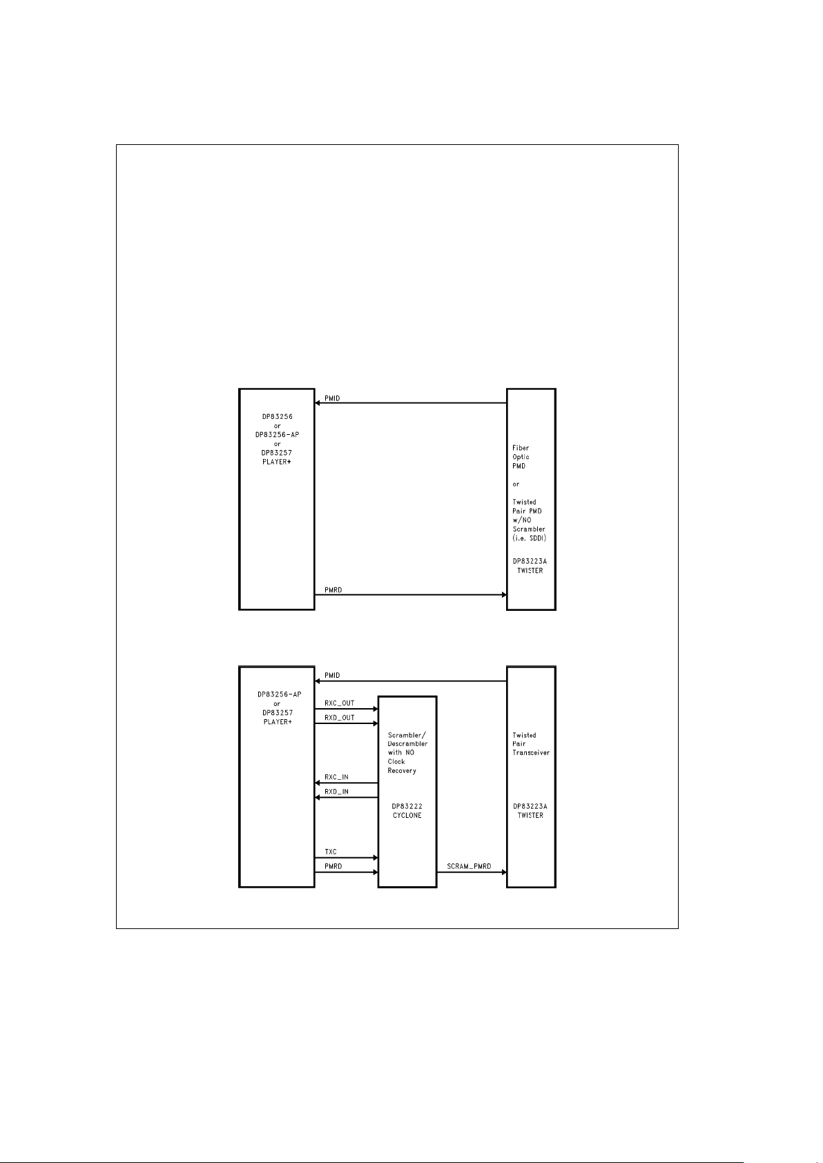
3.0 Functional Description (Continued)
3.8 PMD INTERFACE
The PMD Interface connects the PLAYER
a
device to a
standard FDDI Physical Media Connection such as a fiber
optic transceiver or a copper twisted pair transceiver. It is a
125 MHz full duplex serial connection.
The DP83256 PLAYER
a
device contains one PMD interface. This PMD Interface should be used for all PMD implementations that do not require an external scrambler/
descrambler function, clock recovery function, or clock
generation function, such as a Fiber Optic or Shielded
Twisted Pair (SDDI) PMDs.
The DP83256-AP and DP83257 PLAYER
a
devices contain
two PMD interfaces. The PMD Interface should be used for
all PMD implementations that do not require an external
scrambler/descrambler function, clock recovery function,
or clock generation function, such as a Fiber Optic or
Shielded Twisted Pair (SDDI) PMDs. The second, Alternate
PMD Interface can be used to support Unshielded Twisted
Pair (UTP) PMDs that require external scrambling, and allows implementation with no external clock recovery or
clock generation functions required. See
Figure 3-21.
PLAYERaTO PMD CONNECTIONS
The following figures illustrate how the PLAYERadevice
can be connected to various types of PMDs.
Figure 3-20
shows how the DP83256, DP83256-AP, or
DP83257 PLAYER
a
device is connected to a Fiber Optic
or Shielded Twisted Pair (SDDI) PMD using the Primary
PMD Interface.
Figure 3-21
shows how the DP83256-AP or DP83257
PLAYER
a
device is connected to an Unshielded Twisted
Pair (UTP) PMD using the Alternate PMD Interface.
TL/F/11708– 47
FIGURE 3-20. Fiber Optic or STP PMD Connection
TL/F/11708– 48
FIGURE 3-21. UTP PMD Connections
29

3.0 Functional Description (Continued)
INTERFACE ACTIVATION
The Primary PMD Interface is always enabled.
The Alternate PMD Interface is enabled by programming a
PLAYER
a
register bit. To enable the interface, writea1to
the APMDEN bit in the APMDREG register. The interface is
off by default and should be left that way unless it is being
used.
It will also probably be necessary to enable the Transmit
Clocks when using the Alternate PMD Interface. The Transmit Clocks (TXC) are enabled by writing a 1 to the TXCE bit
in the CGMREG register. The transmit clocks are disabled
by default and should be left that way unless it is being
used.
Note that when the Alternate PMD Interface is active, the
Primary PMD Interface can not be used without the Alternate PMD Interface connections. Also note that the Long
Internal Loopback (LILB) can not be used when the Alternate PMD Interface is activated.
30
 Loading...