

DP8310/DP8311
Octal Latched Peripheral Drivers
General Description
The DP8310 and DP8311 Octal Latched Peripheral Drivers
provide the function of latching eight bits of data with open
collector outputs, each driving up to 100 mA DC with an operating voltage range of 30V. Both devices are designed for
low input currents, high input/output voltages, and feature a
power up clear (outputs off) function.
The DP8310 is positive edge latching. Two active low write/
enable inputs are available forconvenientdatabussingwithout external gating.
The DP8311 is positive edge latching. The active low strobe
input latches data or allows fall through operation when held
at logic “0”. The latches are cleared (outputs off) with a logic
“0” on the clear pin.
Features
n High current, high voltage open collector outputs
n Low current, high voltage inputs
n All outputs simultaneously sink rated current “DC” with
no thermal derating at maximum rated temperature
n Parallel latching or buffering
n Separate active low enables for easy data bussing
n Internal “glitch free” power up clear
n 10%V
CC
tolerance
Applications
n High current high voltage drivers
n Relay drivers
n Lamp drivers
n LED drivers
n TRIAC drivers
n Solenoid drivers
n Stepper motor drivers
n Level translators
n Fiber-optic LED drivers
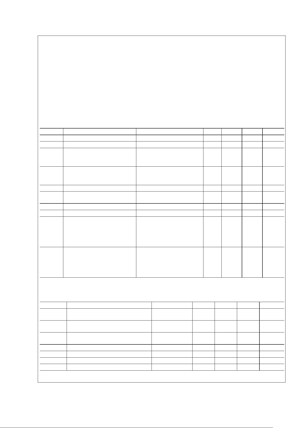
Connection Diagrams
Dual-In-Line Package
DS005246-1
Top View
Dual-In-Line Package
DS005246-2
Top View
Order Number DP8310N or DP8311N
See NS Package Number N20A
February 2000
DP8310/DP8311 Octal Latched Peripheral Drivers
© 2000 National Semiconductor Corporation DS005246 www.national.com
Absolute Maximum Ratings (Note 1)
If Military/Aerospace specified devices are required,
please contact the National Semiconductor Sales Office/
Distributors for availability and specifications.
Supply Voltage 7.0V
Input Voltage 35V
Output Voltage 35V
Maximum Power Dissipation
*
at T
A
=
25˚C
DP8310/DP8311 2005 mW
Storage Temperature Range −65˚C to +150˚C
Lead Temperature (Soldering, 4 sec.) 260˚C
Note:*Derate N20A package 15.4 mW/˚C above T
A
=
25˚C, θJ
A
=
65˚C/W.
Operating Conditions
Min Max Units
Supply Voltage (V
CC
) 4.5 5.5 V
Temperature
DP8310/DP8311 0 +70 ˚C
Input Voltage 30 V
Output Voltage 30 V
DC Electrical Characteristics
DP8310 and DP8311 (Notes 2, 3)
Symbol Parameter Conditions Min Typ Max Units
V
IH
Logical “1” Input Voltage 2.0 V
V
IL
Logical “0” Input Voltage 0.8 V
V
OL
Logical “0” Output Voltage Data outputs latched to
logical “0”, V
CC
=
Min.
DP8310/DP8311 I
OL
=
100 mA 0.35 0.5 V
I
OH
Logical “1” Output Current Data outputs latched to
logical “1”, V
CC
=
Min.
DP8310/DP8311 V
OH
=
30V 2.5 250 µA
I
IH
Logical “1” Input Current V
IH
=
2.7V, V
CC
=
Max 0.1 25 µA
I
I
Input Current at Maximum Input
Voltage
V
IN
=
30V, V
CC
=
Max
1 250 µA
I
IL
Logical “0” Input Current V
IN
=
0.4V, V
CC
=
Max −215 −300 µA
V
clamp
Input Clamp Voltage I
IN
=
12 mA −0.8 −1.5 V
I
CC0
Supply Current, Outputs On Data outputs latched to a
logical “0”. All Inputs are
at logical “1”, V
CC
=
Max.
DP8310 100 152 mA
DP8311 88 125 mA
I
CC1
Supply Current, Outputs Off Data outputs latched to a
logic “1”. Other
conditions same as I
CC0
.
DP8310 40 57 mA
DP8311 25 36 mA
AC Electrical Characteristics
DP8310 only: V
CC
=
4.5V, T
A
=
25˚C
Symbol Parameter Conditions Min Typ Max Units
t
pd0
High to Low Propagation Delay
Write Enable Input to Output
(Figure 1 )
40 120 ns
t
pd1
Low to High Propagation Delay
Write Enable Input to Output
(Figure 1 )
70 150 ns
t
SETUP
Minimum Set-Up Time
Data in to Write Enable Input
t
HOLD
=
0ns
(Figure 1)
45 20 ns
t
pWH,tpWL
Minimum Write Enable Pulse Width
(Figure 1 )
60 25 ns
t
THL
High to Low Output Transition Time
(Figure 1 )
16 35 ns
t
TLH
Low to High Output Transition Time
(Figure 1 )
38 70 ns
C
IN
“N” Package (Note 4) 5 15 pF
DP8310/DP8311
www.national.com 2
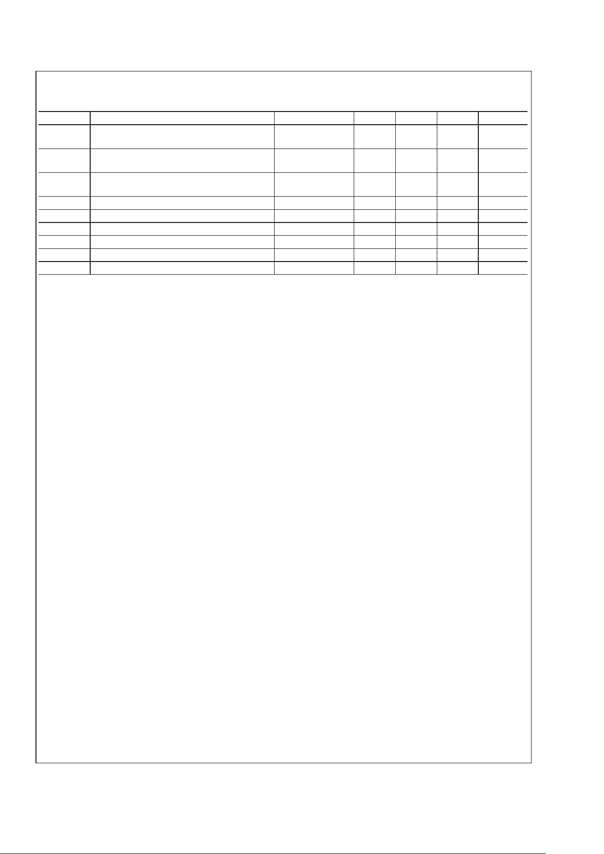
AC Electrical Characteristics
DP8311 only: V
CC
=
5V, T
A
=
25˚C
Symbol Parameter Conditions Min Typ Max Units
t
pd0
High to Low Propagation Delay
Data In to Output
(Figure 2 )
30 60 ns
t
pd1
Low to High Propagation Delay
Data to Output
(Figure 2)
70 100 ns
t
SETUP
Minimum Set-Up Time
Data in to Strobe Input
t
HOLD
=
0ns
(Figure 2 )
0 −25 ns
t
pWL
Minimum Strobe Enable Pulse Width
(Figure 2 )
60 35 ns
t
pdC
Propagation Delay Clear to Data Output
(Figure 2 )
70 135 ns
t
pWC
Minimum Clear Input Pulse Width
(Figure 2 )
60 25 ns
t
THL
High to Low Output Transition Time
(Figure 2 )
20 35 ns
t
TLH
Low to High Output Transition Time
(Figure 2 )
38 60 ns
C
IN
Input Capacitance — Any Input (Note 4) 5 15 pF
Note 1: “AbsoluteMaximum Ratings” are those values beyond which the safety of the device cannot be guaranteed. Except for “Operating TemperatureRange” they
are not meant to imply that the devices should be operated at these limits. The table of “Electrical Characteristics” provides conditions for actual device operation.
Note 2: Unless otherwise specified min/max limits apply across the 0˚C to +70˚C for the DP8310/DP8311. All typical values are for T
A
=
25˚C, V
CC
=
5V.
Note 3: All currents into device pins shown as positive, out of device pins as negative, all voltages referenced to ground unless otherwise noted.
Note 4: Input capacitance is guaranteed by periodic testing. f
TEST
=
10 kHz at 300 mV, T
A
=
25˚C.
DP8310/DP8311
www.national.com3
 Loading...