NSC DP8224N Datasheet

DP8224 Clock Generator and Driver
DP8224 Clock Generator and Driver
June 1986
General Description
The DP8224 is a clock generator/driver contained in a standard, 16-pin dual-in-line package. The chip, which is fabricated using Schottky Bipolar technology, generates clocks
and timing for the 8080A microcomputer family.
Included in the DP8224 is an oscillator circuit that is controlled by an external crystal, which is selected by the designer to meet a variety of system speed requirements. Also
included in the chip are circuits that provide: a status strobe
for the DP8228 or DP8238 system controllers, power-on reset for the 8080A microprocessor, and synchronization of
the READY input to the 8080A.
Features
Y
Crystal-controlled oscillator for stable system operation
Y
Single chip clock generator and driver for 8080A microprocessor
Y
Provides status strobe for DP8228 or DP8238 system
controllers
Y
Provides power-on reset for 8080A microprocessor
Y
Synchronizes READY input to 8080A microprocessor
Y
Provides oscillator output for synchronization of external circuits
Y
Reduces system component count
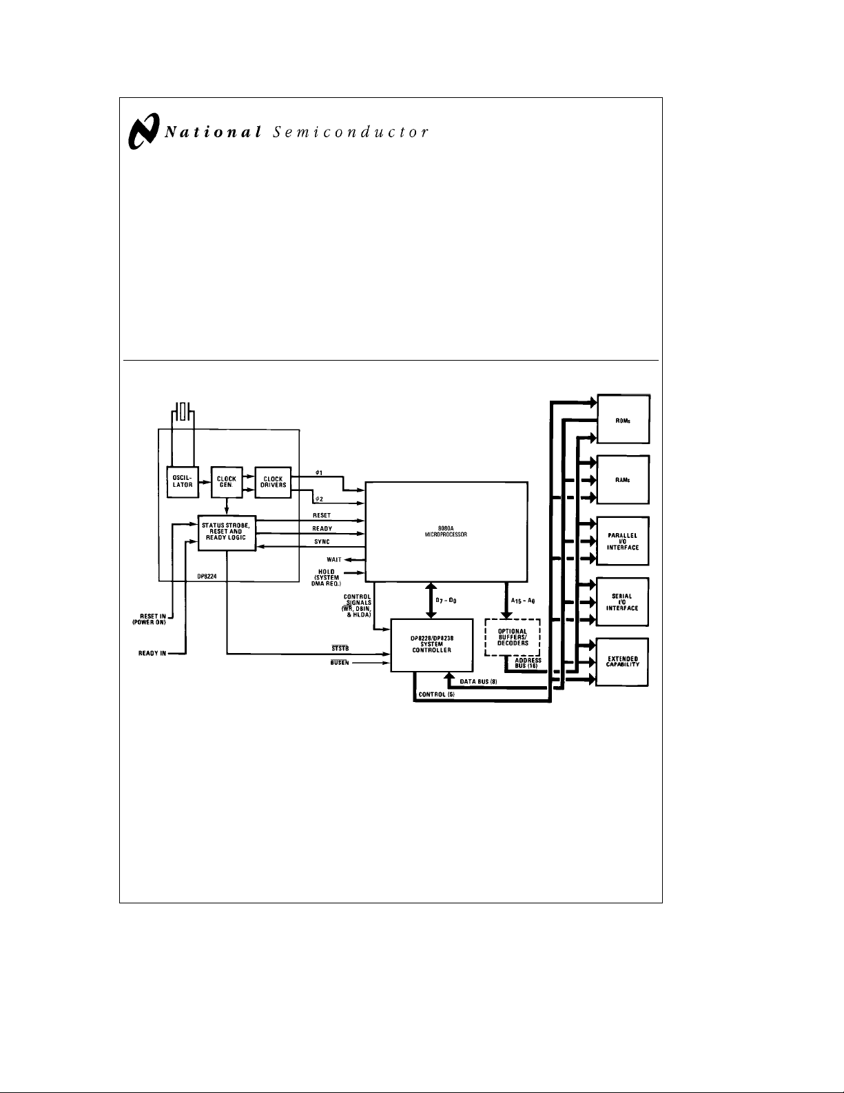
8080A Microcomputer Family Block Diagram
TL/F/8752– 1
C
1995 National Semiconductor Corporation RRD-B30M105/Printed in U. S. A.
TL/F/8752

Absolute Maximum Ratings (Note 2)
If Military/Aerospace specified devices are required,
please contact the National Semiconductor Sales
Office/Distributors for availability and specifications.
Supply Voltage
V
CC
V
DD
Input Voltage
Storage Temperature Range
b
1V toa5.5V
b
65§Ctoa150§C
7V
15V
Operating Conditions
Supply Voltage
V
CC
V
DD
Temperature (T
)0
A
Min Max Units
4.75 5.25 V
11.4 12.6 V
a
70
C
§
Maximum Power Dissipation* at 25§C
Cavity Package 1509 mW
Molded Package 1476 mW
Lead Temperature (Soldering, 4 seconds) 260
* Derate cavity package 10.1 mW/§C above 25§C; derate molded package
11.8 mW/
C above 25§C.
§
C
§
Electrical Characteristics (Note 3)
Symbol Parameter Conditions Min Typ Max Units
I
F
I
R
V
C
V
IL
V
IH
Input Current Loading V
Input Leakage Current V
Input Forward Clamp Voltage I
Input ‘‘Low’’ Voltage V
Input ‘‘High’’ Voltage RESIN Input 2.6 V
e
0.45V
F
e
5.25V 10 mA
R
eb
5mA
C
e
5V 0.8 V
CC
All Other Inputs 2.0 V
b
V
V
IH
V
OL
RESIN Input Hysteresis V
IL
Output ‘‘Low’’ Voltage
(w1, w2), Ready, Reset STSTB
Osc., w2 (TTL) I
Osc., w2 (TTL) I
V
OH
Output ‘‘High’’ Voltage
w1, w2I
Ready, Reset I
Osc., w2 (TTL), STSTB
I
SC
Output Short-Circuit Current V
(All Low Voltage Outputs Only),
e
5V 0.25 V
CC
e
I
2.5 mA 0.45 V
OL
e
10 mA 0.45 V
OL
e
15 mA 0.45 V
OL
eb
100 mA 9.4 V
OH
eb
100 mA 3.6 V
OH
eb
I
1 mA 2.4 V
OH
e
O
0V, V
CC
e
5V
b
10
(Note 1)
I
CC
I
DD
Note 1: Cautionbw1 and w2 output drivers do not have short circuit protection.
Note 2: ‘‘Absolute Maximum Ratings’’ are those values beyond which the safety of the device cannot be guaranteed. Except for ‘‘Operating Temperature Range’’
they are not meant to imply that the devices should be operated at these limits. The table of ‘‘Electrical Characteristics’’ provides conditions for actual device
operation.
Note 3: Unless otherwise specified min/max limits apply across the 0
e
12V.
V
DD
Power Supply Current 115 mA
Power Supply Current 12 mA
Ctoa70§C range for the DP8224. All typical values are for T
§
b
0.25 mA
b
1.0 V
b
60 mA
e
25§C, V
A
e
5V, and
CC
Crystal Requirements*
Tolerance 0.005% at 0§Ctoa70§C
Resonance Fundamental
Load Capacitance 20 pF to 30 pF
*It is good design practice to ground the case of the crystal
**With tank circuit, use 3rd overtone mode
Equivalent Resistance 75X to 20X
Power Dissipation (Min) 4 mW
2

Switching Characteristics (Note 3)
Symbol Parameter Conditions Min Typ Max Units
t
w1
t
w2
t
D1
t
D2
t
D3
t
r
t
f
t
Dw2
t
DSS
t
PW
t
DRS
t
DRH
t
DR
t
CLK
f
MAX
C
IN
w1 Pulse Width
w2 Pulse Width
w1tow2 Delay
w2tow1 Delay
w1tow2 Delay
w1 and w2 Rise Time 20 ns
w1 and w2 Fall Time 20 ns
w2tow2 (TTL) Delay w2 TTL, C
w2 to STSTB Delay
STSTB Pulse Width
RDYIN Set-Up Time to Status Strobe
RDYIN Hold Time After STSTB
READY or RESET to w2 Delay Ready and Reset, C
CLK Period
Maximum Oscillating Frequency 27 MHz
Input Capacitance V
e
C
20 pF to 50 pF
L
e
30 pF,
L
e
300X,R2e600X
R1
,C
e
15 pF
L
STSTB
R1e2kX,R2e4kX
DD
L
e
12V,
e
2kX,R2e4kX
R1
e
5V, V
CC
e
V
BIAS
2.5V, fe1 MHz
e
10 pF,
2t
CY
b
20 ns
9
5t
CY
b
35 ns
9
0ns
2t
CY
b
14 ns
9
2t
CY
9
b
515ns
6t
CY
b
30
9
t
CY
b
15 ns
9
4t
CY
b
50
9
4t
CY
9
4t
CY
b
25 ns
9
2t
CY
a
20 ns
9
6t
CY
9
ns
ns
ns
t
CY
9
ns
8pF
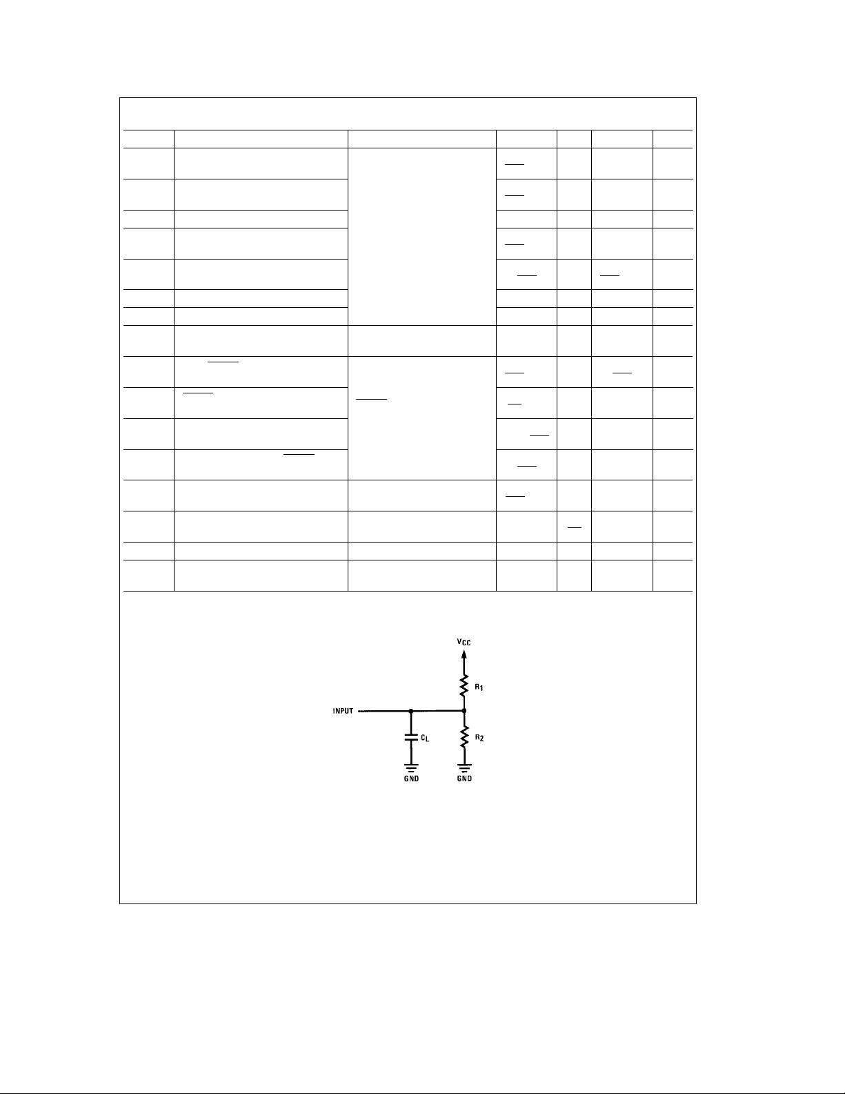
Test Circuit
TL/F/8752– 2
3
 Loading...