NSC DP8212N Datasheet

DP8212/DP8212M 8-Bit Input/Output Port
DP8212/DP8212M 8-Bit Input/Output Port
June 1988
General Description
The DP8212/DP8212M is an 8-bit input/output port contained in a standard 24-pin dual-in-line package. The device,
which is fabricated using Schottky Bipolar technology, is
part of National Semiconductor’s 8080A support family. The
DP8212/DP8212M can be used to implement latches, gated buffers, or multiplexers. Thus, all of the major peripheral
and input/output functions of a microcomputer system can
be implemented with this device.
The DP8212/DP8212M includes an 8-bit latch with
TRI-STATE
trol logic. Also included is a service request flip-flop for the
output buffers, and device selection and con-
É
Features
Y
8-Bit data latch and buffer
Y
Service request flip-flop for generation and control of
interrupts
Y
0.25 mA input load current
Y
TRI-STATE TTL output drive capability
Y
Outputs sink 15 mA
Y
Asynchronous latch clear
Y
3.65V output for direct interface to INS8080A
Y
Reduces system package count by replacing buffers,
latches, and multiplexers in microcomputer systems
generation and control of interrupts to the microprocessor.
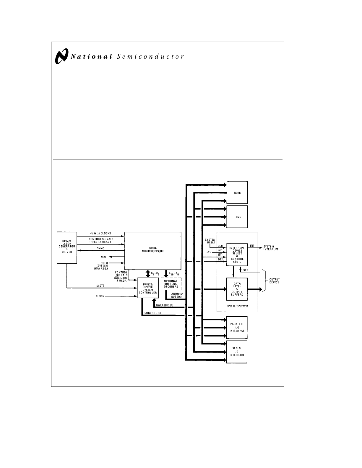
8080A Microcomputer Family Block Diagram
TL/F/6824– 1
TRI-STATEÉis a registered trademark of National Semiconductor Corp.
C
1995 National Semiconductor Corporation RRD-B30M105/Printed in U. S. A.
TL/F/6824

Absolute Maximum Ratings
If Military/Aerospace specified devices are required,
please contact the National Semiconductor Sales
Office/Distributors for availability and specifications.
Storage Temperature
All Output or Supply Voltages
All Input Voltages
Output Currents 125 mA
Maximum Power Dissipation* at 25§C
Cavity Package 1903 mW
Molded Package 2005 mW
*Derate cavity package 12.7 mW/§C above 25§C; derate molded package
16.0 mW/
C above 25§C.
§
b
65§Ctoa160§C
b
0.5V toa7V
b
1.0V to 5.5V
Operating Conditions
Supply Voltage (V
DP8212M 4.50 5.50 V
CC
)
DP8212 4.75 5.25 V
Operating Temperaure (TA)
DP8212M
DP8212 0
Note:
Maximum ratings indicate limits beyond which permanent damage may occur. Continuous operation at these limits is not intended and should be limited to those conditions
specified under DC electrical characteristics.
Min Max Units
DC
DC
b
a
55
125
a
75
§
§
C
C
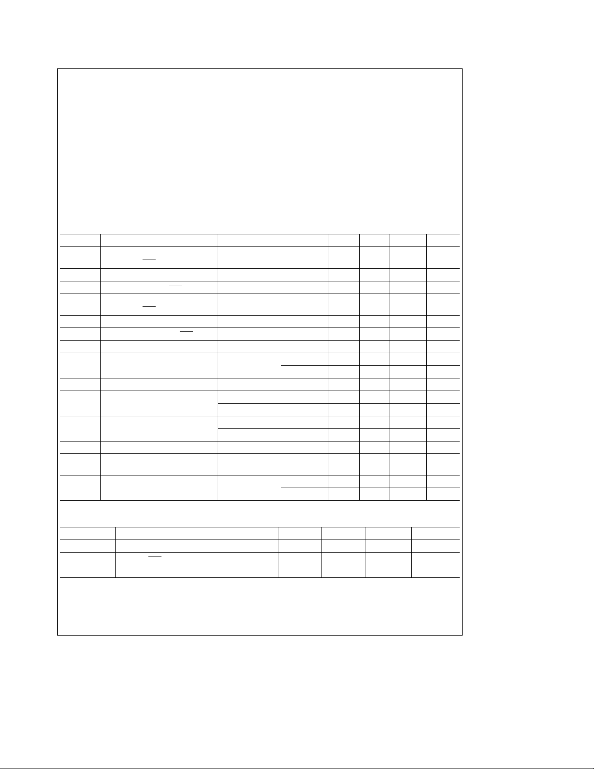
Electrical Characteristics Min
s
T
s
Max, MinsV
A
s
Max, unless otherwise noted
CC
Symbol Parameter Conditions Min Typ Max Units
I
F
I
F
I
F
I
R
I
R
I
R
V
C
Input Load Current, V
STB, DS2, CLR
,DI1–DI8Inputs
Input Load Current, MD Input V
Input Load Current, DS1 Input V
Input Leakage Current V
STB, DS2, CLR,DI1–DI8Inputs
Input Leakage Current, MD Input V
Input Leakage Current, DS1 Input V
Input Forward Voltage Clamp I
e
0.45V
F
e
0.45V
F
e
0.45V
F
e
VCCMax
R
e
VCCMax 30 mA
R
e
VCCMax 40 mA
R
eb
5mA
C
b
0.25 mA
b
0.75 mA
b
10 mA
b
1.0 mA
1V
VILInput ‘‘Low’’ Voltage DP8212M 0.08 V
DP8212 0.85 V
V
IH
V
OL
V
OH
I
SC
I
l
l
O
I
CC
Input ‘‘High’’ Voltage 2.0 V
Output ‘‘Low’’ Voltage I
Output ‘‘High’’ Voltage I
Short-Circuit Output Current V
Output Leakage Current, High V
Impedance State
e
10 mA DP8212M 0.45 V
OL
e
I
15 mA DP8212 0.45 V
OL
e
0.5 mA DP8212M 3.40 4.0 V
OH
e
I
1.0 mA DP8212 3.65 4.0 V
OH
e
O
e
O
e
0V, V
CC
5V
0.45V/VCCMax
b
15
b
75 mA
20 mA
Power Supply Current DP8212M 90 145 mA
DP8212 90 130 mA
Capacitance* F
e
1 MHz, V
BIAS
e
2.5V, V
CC
e
5V, T
e
25§C
A
Symbol Parameter Min Typ Max Units
C
IN
C
IN
C
OUT
*This parameter is sampled and not 100% tested.
DS1, MD Input Capacitance 9 12 pF
DS2, CLR, STB, DI1–DI8Input Capacitance 5 9 pF
DO1–DO8 Output Capacitance 8 12 pF
2

s
Switching Characteristics Min
s
T
A
Max, MinsV
Symbol Parameter Conditions
s
Max
CC
DP8212M DP8212
Min Max Min Max
t
PW
t
PD
t
WE
t
SET
t
H
t
R
t
S
t
E
t
C
Note 1: C
Note 2: C
t
E (DISABLE)CL
Pulse Width 40 30 ns
Data to Output Delay (Note 1) 30 30 ns
Write Enable to Output Delay (Note 1) 50 40 ns
Data Set-Up Time 20 15 ns
Data Hold Time 30 20 ns
Reset to Output Delay (Note 1) 55 40 ns
Set to Output Delay (Note 1) 35 30 ns
Output Enable/Disable Time (Note 2) 50 45 ns
Clear to Output Delay (Note 1) 65 55 ns
e
30 pF
L
e
30 pF except for DP8212M
L
e
5pF
Switching Conditions
1. Input Pulse Amplitudee2.5V.
2. Input Rise and Fall Timese5 ns.
3. Between 1V and 2V Measurements made at 1.5V with 15 mA & 30 pF Test Load.
includes jig and probe capacitance.
4. C
L
e
5. C
30 pF.
L
e
6. C
30 pF except for DP8212M t
L
E (DISABLE)CL
e
5pF
Units
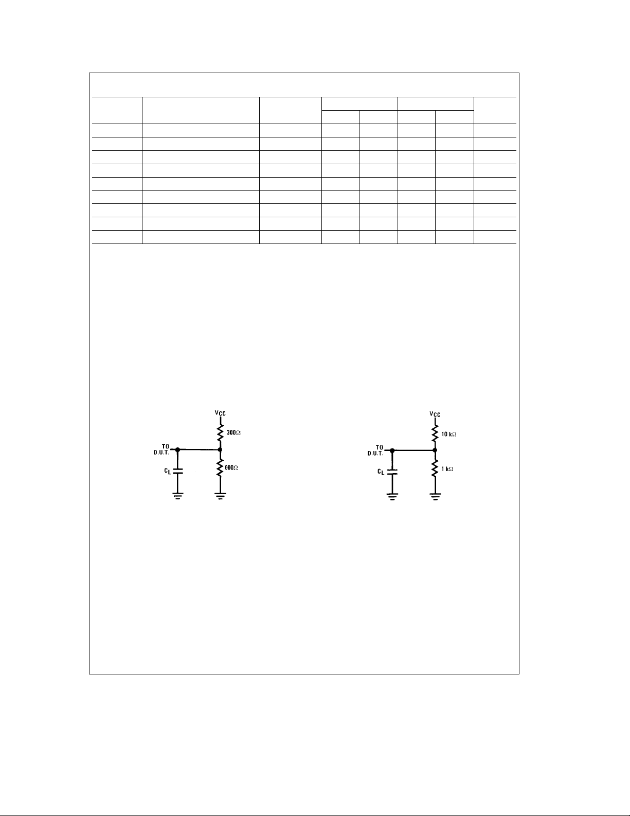
Test Load
TL/F/6824– 2
Alternate Test Load
(Refer to Timing Diagram)
TL/F/6824– 3
3
 Loading...